SCT/Pixel TIM-ROD Interface Specification
December 3, 2002
Draft 0.9 by John Lane
Abstract
This document is a preliminary draft of the SCT/Pixel
interface specification between TIM and ROD. Feedback is welcome.
Introduction
The TTC Interface Module (TIM) interfaces to a crate
of Read-Out Drivers (RODs) via a custom backplane.
This specification should satisfy the interface requirements set out in
the ROD requirements document [ref. ROD_requirements]
and the TIM requirements document
[ref. TIM_requirements].
Pin assignments and other details are given in the backplane specification
[ref. ROD_backplane].
Signals
- The TIM transmits the following signals to each ROD slot:
| Name | Level | Sense | Description
|
|---|
| TTC0-TTC7 | 3V | active low | TTC signals synchronized to clock
|
The Timing, Trigger and Control (TTC) signals, TTC0-TTC7,
should be generated by programmable logic on the TIM and
received by programmable logic on the ROD, allowing the meaning
of the signals to be changed as the TIM and ROD designs solidify.
- Signal assignments for TTC0 - TTC7:
| Name | Signal | Comment
|
|---|
| TTC0 | L1Accept | Level-1 trigger Accept decision
|
| TTC1 | ECReset | Event Counters (L1ID) are reset periodically
|
| TTC2 | BCReset | Bunch Counters (BCID) are reset once per LHC orbit
|
| TTC3 | CAL | Calibration pulse command for front-end amplifiers
|
| TTC4 | SerialID | 1 start bit + 24 L1ID bits + 12 BCID bits
|
| TTC5 | SerialTT | 1 start bit + 8 Trigger Type bits + 2 reserved bits
|
| TTC6 | reserved | spare, eg maybe a separate periodic reset signal
|
| TTC7 | unused | spare
|
All the signals above are active-low; unused signals are held high.
The command signals L1Accept, ECReset, BCReset and CAL are active for
one clock cycle. In response to these signals, the ROD generates the
control bit sequence of the front-end protocol appropriate to the
module type: strips (SCT) or pixels.
The data values within SerialID and SerialTT are sent with the
least significant bit first. The start bit has a value of 1 (low),
which is guaranteed to be preceded by a 0 (high).
- The TIM receives the following signal from each ROD slot:
| Name | Level | Sense | Description
|
|---|
| BUSY | 3V | active low | asynchronous ROD busy signal
|
Signal Relationships
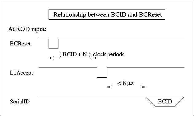
- BCReset is sent early by N clock periods,
because its front-end protocol is N+1 bits long (instead of 1 bit),
assuming the ROD latency is the same for BCReset and L1Accept.
For SCT, N = 6, and for Pixel, N = 8.
- The ROD receives the ATLAS-wide BCID and L1ID values:
these are sent on to the Read-Out Buffer.
- The front-end BCID is offset from the ROD value:
FE_BCID = ROD_BCID + M
because the L1Accept front-end protocol is M+1 bits (instead of 1 bit),
assuming the ROD latency is the same for BCReset and L1Accept.
For SCT, M = 2, and for Pixel, M = 4.
- The ROD_BCID value is in the range 0 - 3563, reset by BCReset,
when running with the LHC orbit cycle. If BCReset is not generated,
ROD_BCID is in the range 0 - 4095.
- The first L1Accept trigger after an ECReset has an L1ID value of 0.
This is determined by the TTC system receiver (TTCrx).
- The SerialID and SerialTT values are independently queued before
transmission for up to 8us and 10us after the L1Accept, respectively;
either may be transmitted first for a given event.
These latency limits assume the Level-1 trigger limits the number
of L1Accepts in some period to 8.
- The CAL command is issued a programmable number of clock periods
before its L1Accept.
- The timing relationships between the command signals should respect
the front-end protocol: one command at a time, each taking a number
of clock periods. Protection on TIM introduces deadtime except for
commands generated by the TTC system or the TIM sequencer.
Timing
- The clock for each ROD is passed from its back-of-crate (BOC) card.
- The active edge of the clock is the rising edge.
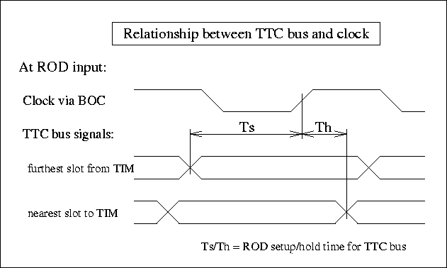
- At each ROD slot, the TTC0-TTC7 signals from the TIM must satisfy
the setup and hold timing specification relative to the active edge
of the clock. The TIM adjustment takes into account the delay of
buffering the clock on the BOC and the timing skew due to the backplane.
The setup and hold times at ROD input must be greater than
5ns and 0ns respectively.
- Latency adjustment to the command signals L1Accept, ECReset, BCReset and
CAL is done in the TTC system.
- The ROD BUSY signal is asynchronous.
Electrical Notes
- TTC0-TTC7 are bussed and terminated on the backplane;
only the trace end that is most distant from the driver is terminated
if the TIM slot is at the other end.
- RODs should minimally load TTC0-TTC7 so that transmission line
characteristics are affected as little as possible by the presence
or absence of RODs.
- Negative (active-low) logic is preferred for low duty-cycle signals
(all signals).
- The ROD BUSY from each slot is routed to a separate pin at the TIM slot.
- The TIM should pull all BUSY signals high (inactive) through a resistor,
or they should be similarly terminated on the backplane,
to indicate empty ROD slots as not busy.
References
On the Web via:  ATLAS -> Inner Detector -> SCT -> Off Detector

ROD_backplane    Off Detector -> ROD crate backplane
ROD_requirements Off Detector -> ROD -> Functional Requirements Document
TIM_requirements http://www.hep.ucl.ac.uk/~jbl/SCT/TIM_requirements.html

History:

0.1 29Apr98 UCI First draft
0.3 11Nov98 UCI http://positron.ps.uci.edu/~pier/ROD/pdf/RODtofromTTC1.PDF
0.4 29Jul99 JBL New version, separating ROD from BOC
0.5  1Nov99 JBL Define Serial order, start bit, clock edge (23Sep99 mtg)
0.6  9Dec99 JBL Update References
0.7 25Jul00 JBL Add Signal Relationships, diagrams
0.8 29Sep00 JBL Rewrite Relationships; define setup & hold; Pixel too
0.9  3Dec02 JBL First L1ID is 0
    22Jun04 JBL Remove broken off-detector link
Last update: 22 June 2004
by John Lane (UCL) email:
jbl@hep.ucl.ac.uk
http://www.hep.ucl.ac.uk/~jbl/SCT/TIM_interface_ROD.html