Proton Calorimetry/Experimental Runs/2021/Apr22: Difference between revisions
SaadShaikh (talk | contribs) No edit summary |
SaadShaikh (talk | contribs) No edit summary |
||
| (5 intermediate revisions by the same user not shown) | |||
| Line 4: | Line 4: | ||
'''Notes''' | '''Notes''' | ||
*D27 is an electronically noisy lab whereas D109 is a quieter office (though still not a perfectly shielded environment). | |||
*Test 2 DDC232 boards coupled to scintillator stack. | *Test 2 DDC232 boards coupled to scintillator stack. | ||
*CMOS sensor coupled to scintillator stack on perpendicular face. | *CMOS sensor coupled to scintillator stack on perpendicular face. | ||
*Both CMOS sensor daughter board and DDC232 Nexys Video board in detector enclosure. | *Both CMOS sensor daughter board and DDC232 Nexys Video board in detector enclosure. | ||
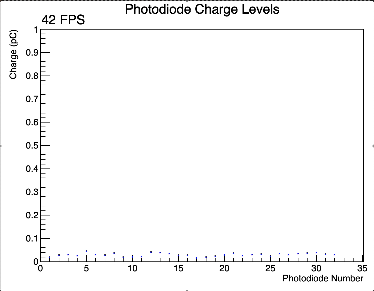
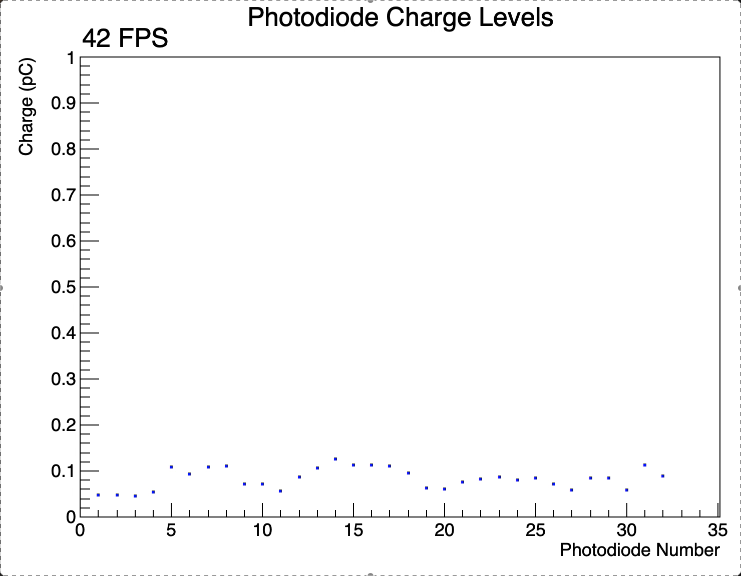
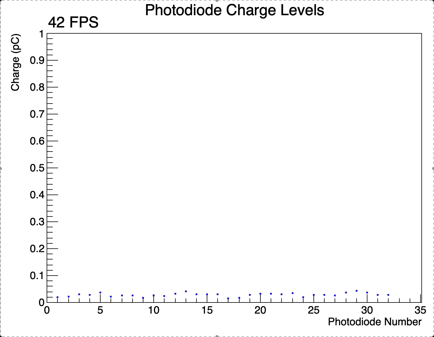
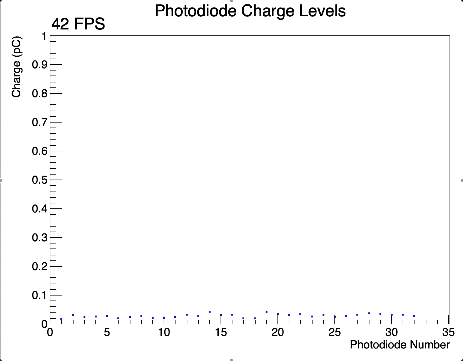
*In all runs, an integration time of 170us is used. | *In all runs, an integration time of 170us is used. | ||
*Video steps through individual consecutive acquisitions at frame rate shown. | *Video steps through individual consecutive acquisitions at frame rate shown. Each frame represents 170us in time. | ||
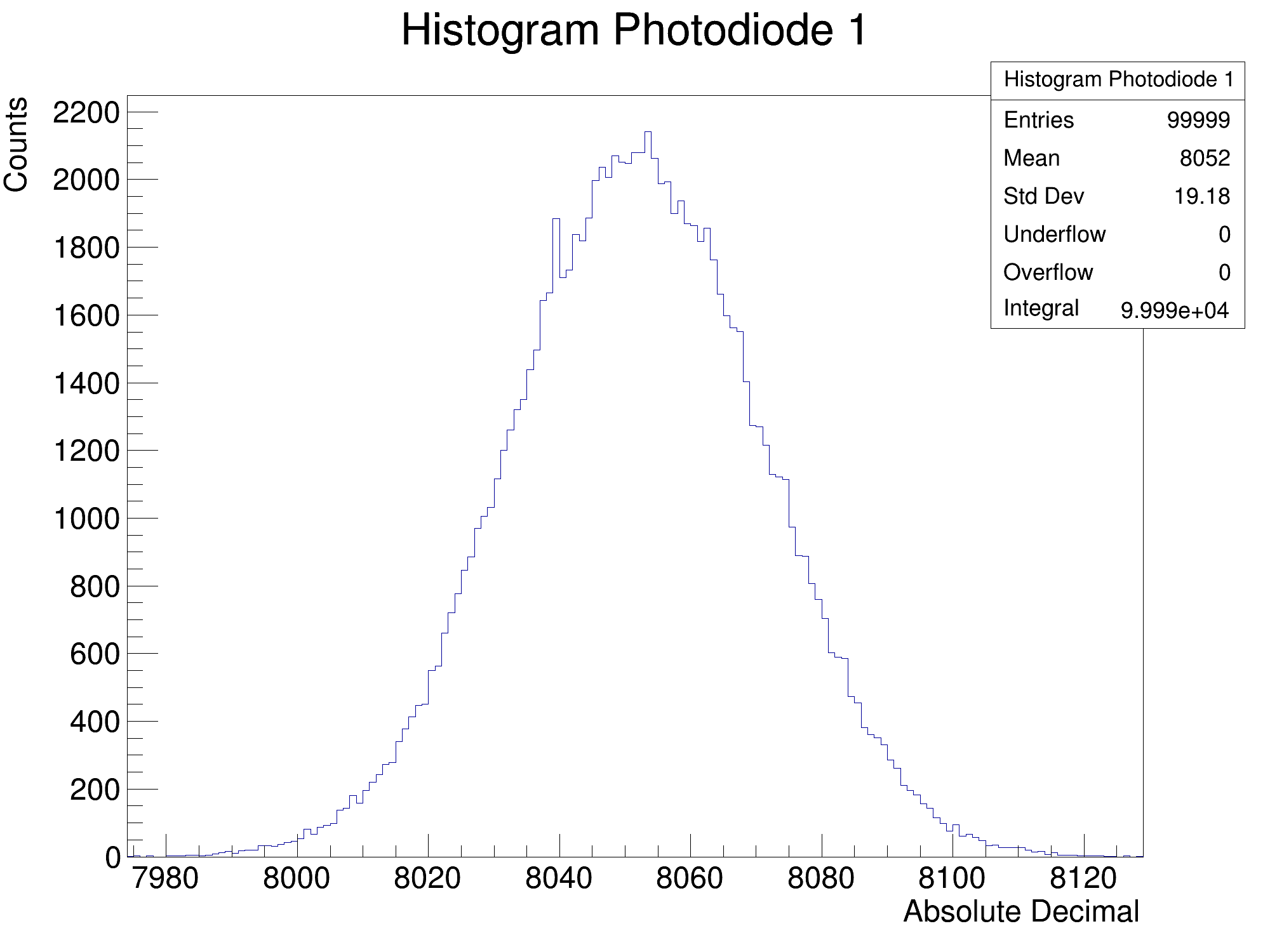
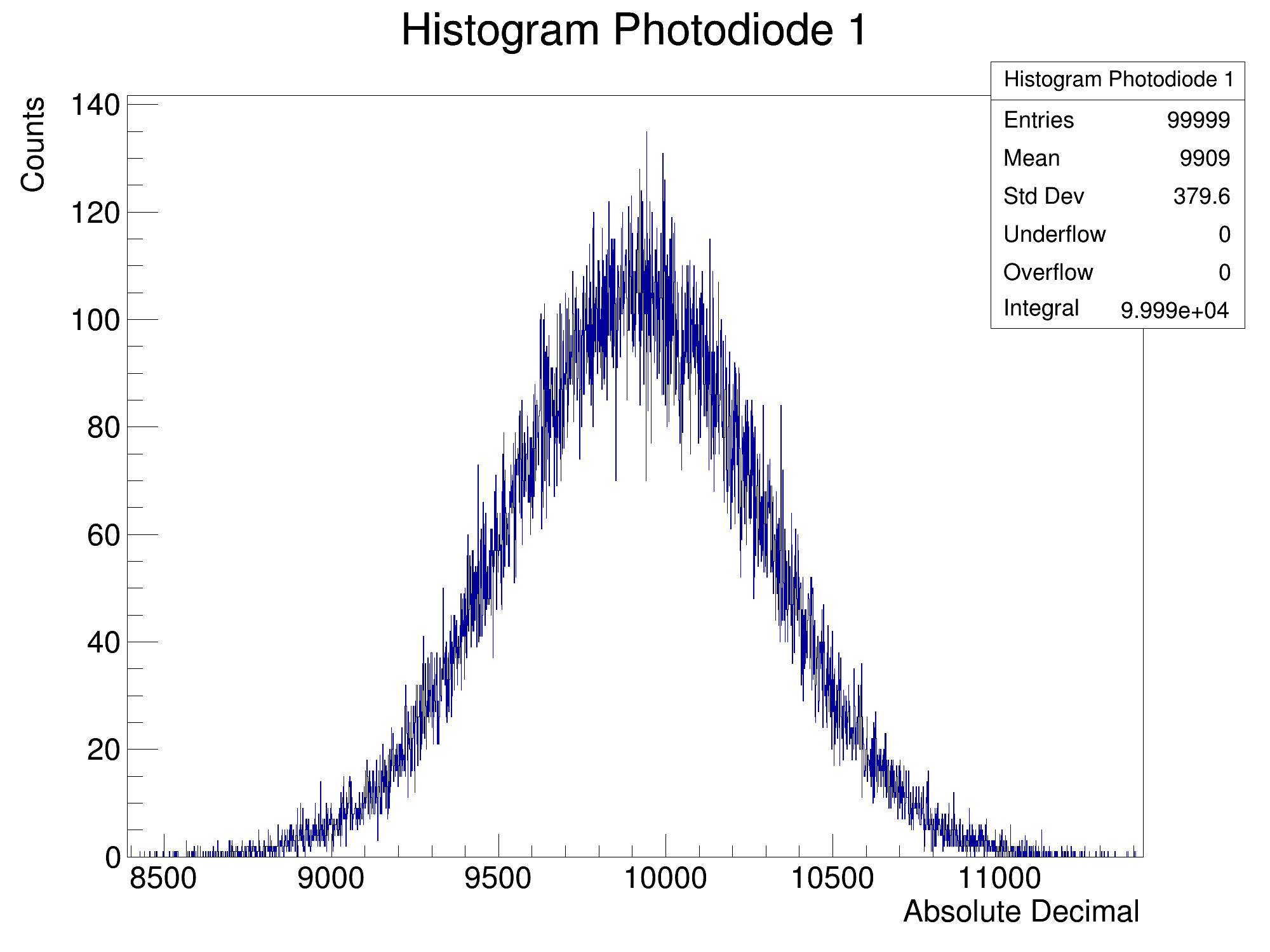
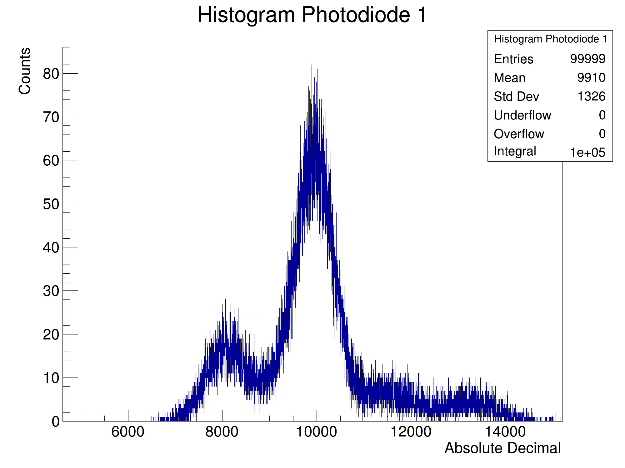
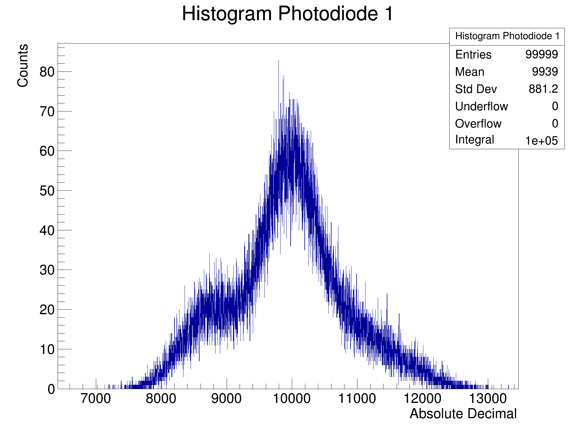
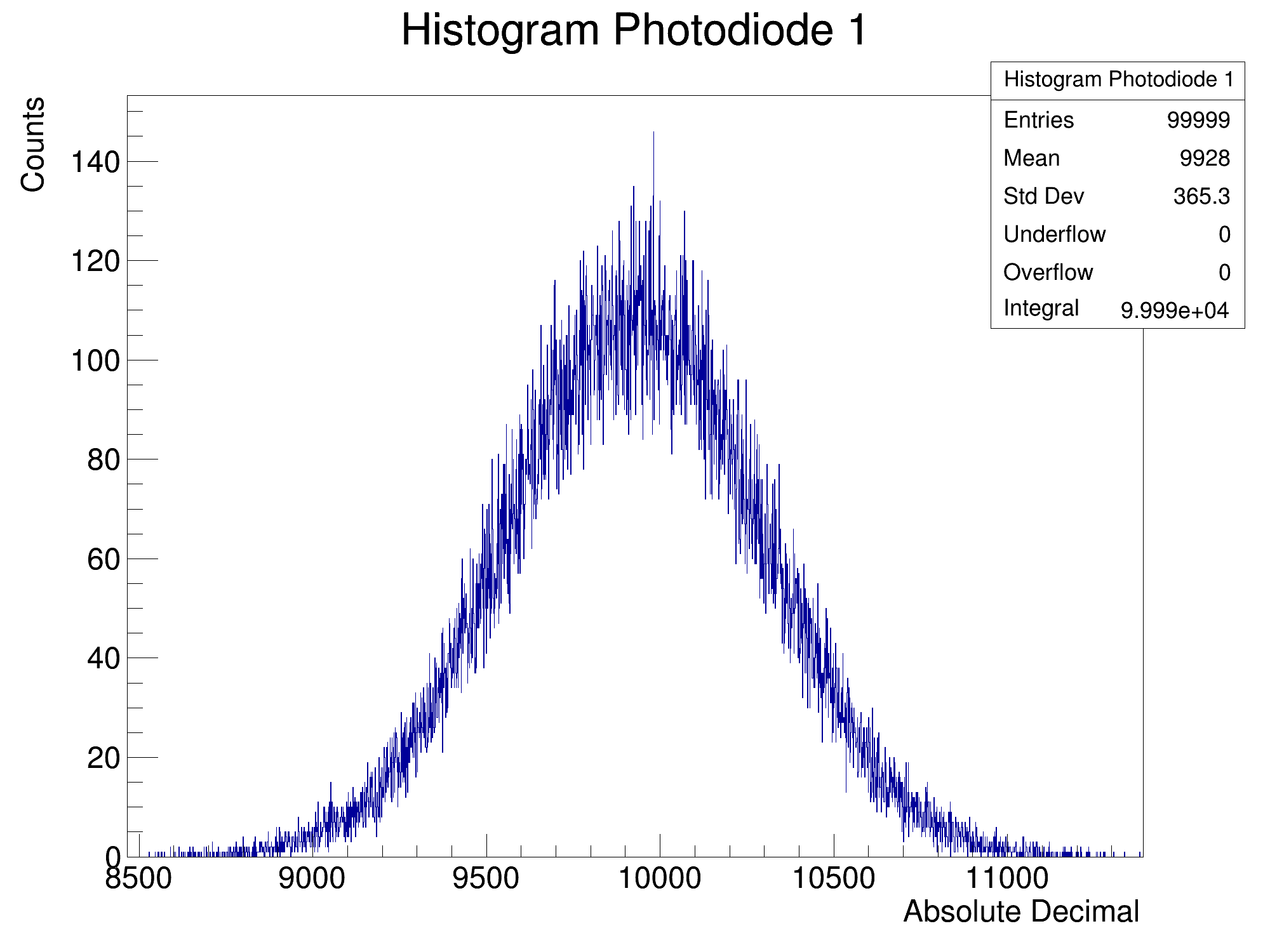
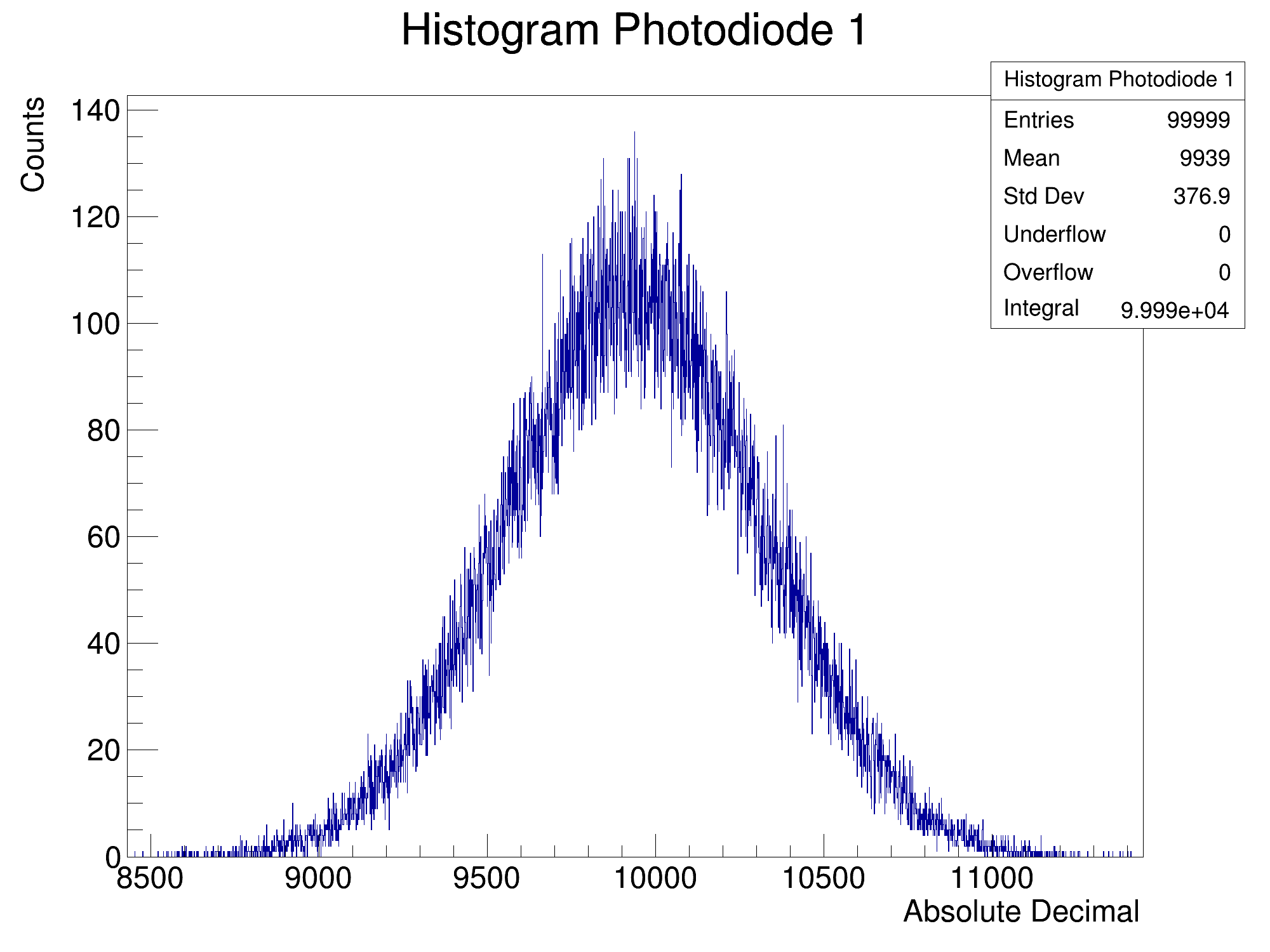
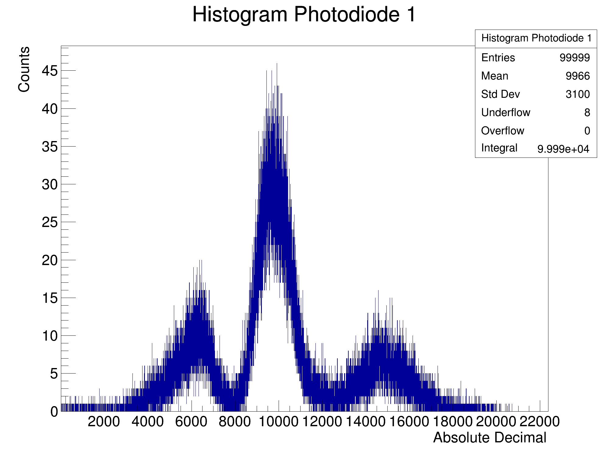
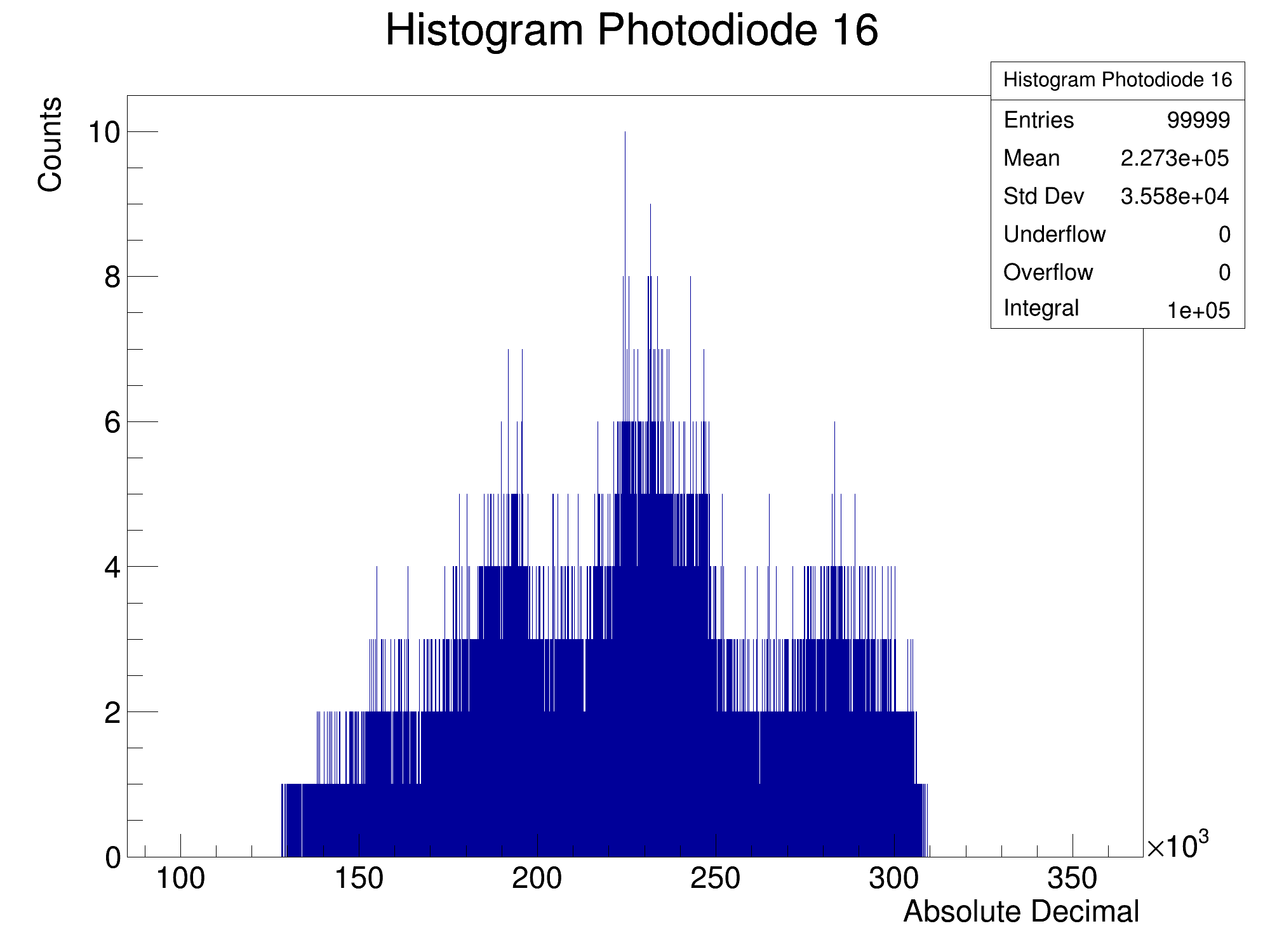
*Histogram of one photodiode also provided. Expect to see clean gaussian shape if no external noise is being picked up. | *Histogram of one photodiode also provided. Expect to see clean gaussian shape if no external noise is being picked up. | ||
**Signal photodiode shown for Run 14. | **Signal photodiode shown for Run 14. | ||
| Line 21: | Line 22: | ||
!Video | !Video | ||
|- | |- | ||
|1 || | |1 || D27, CMOS on, 350pC || | ||
<div class="image150px" style="text-align: center;"> | <div class="image150px" style="text-align: center;"> | ||
[http://www.hep.ucl.ac.uk/pbt/wikiData/movies/DDC232/210422/Histograms/Run001.png http://www.hep.ucl.ac.uk/pbt/wikiData/movies/DDC232/210422/Histograms/Run001.png] | [http://www.hep.ucl.ac.uk/pbt/wikiData/movies/DDC232/210422/Histograms/Run001.png http://www.hep.ucl.ac.uk/pbt/wikiData/movies/DDC232/210422/Histograms/Run001.png] | ||
| Line 29: | Line 30: | ||
</div> | </div> | ||
|- | |- | ||
|2 || | |2 || D27, CMOS on, 12.5pC || | ||
<div class="image150px" style="text-align: center;"> | <div class="image150px" style="text-align: center;"> | ||
[http://www.hep.ucl.ac.uk/pbt/wikiData/movies/DDC232/210422/Histograms/Run002.png http://www.hep.ucl.ac.uk/pbt/wikiData/movies/DDC232/210422/Histograms/Run002.png] | [http://www.hep.ucl.ac.uk/pbt/wikiData/movies/DDC232/210422/Histograms/Run002.png http://www.hep.ucl.ac.uk/pbt/wikiData/movies/DDC232/210422/Histograms/Run002.png] | ||
</div> | </div> | ||
|| <div class="image150px" style="text-align: center;"> | || <div class="image150px" style="text-align: center;"> | ||
[http://www.hep.ucl.ac.uk/pbt/wikiData/movies/DDC232/210422/Run002.mp4 | [http://www.hep.ucl.ac.uk/pbt/wikiData/movies/DDC232/210422/Run002.mp4 http://www.hep.ucl.ac.uk/pbt/wikiData/movies/DDC232/210422/Thumbnails/Run002.png] | ||
http://www.hep.ucl.ac.uk/pbt/wikiData/movies/DDC232/210422/Thumbnails/Run002.png] | |||
</div> | </div> | ||
|- | |- | ||
|3 || | |3 || D27, CMOS off, 350pC || | ||
<div class="image150px" style="text-align: center;"> | |||
[http://www.hep.ucl.ac.uk/pbt/wikiData/movies/DDC232/210422/Histograms/Run003.png http://www.hep.ucl.ac.uk/pbt/wikiData/movies/DDC232/210422/Histograms/Run003.png] | |||
</div> | |||
|| <div class="image150px" style="text-align: center;"> | |||
[http://www.hep.ucl.ac.uk/pbt/wikiData/movies/DDC232/210422/Run003.mp4 http://www.hep.ucl.ac.uk/pbt/wikiData/movies/DDC232/210422/Thumbnails/Run003.png]</div> | [http://www.hep.ucl.ac.uk/pbt/wikiData/movies/DDC232/210422/Run003.mp4 http://www.hep.ucl.ac.uk/pbt/wikiData/movies/DDC232/210422/Thumbnails/Run003.png]</div> | ||
|- | |- | ||
|4 || | |4 || D27, CMOS off, 12.5pC || | ||
<div class="image150px" style="text-align: center;"> | |||
[http://www.hep.ucl.ac.uk/pbt/wikiData/movies/DDC232/210422/Histograms/Run004.png http://www.hep.ucl.ac.uk/pbt/wikiData/movies/DDC232/210422/Histograms/Run004.png] | |||
</div> | |||
|| <div class="image150px" style="text-align: center;"> | |||
[http://www.hep.ucl.ac.uk/pbt/wikiData/movies/DDC232/210422/Run004.mp4 http://www.hep.ucl.ac.uk/pbt/wikiData/movies/DDC232/210422/Thumbnails/Run004.png]</div> | [http://www.hep.ucl.ac.uk/pbt/wikiData/movies/DDC232/210422/Run004.mp4 http://www.hep.ucl.ac.uk/pbt/wikiData/movies/DDC232/210422/Thumbnails/Run004.png]</div> | ||
|- | |- | ||
|5 || | |5 || D109, CMOS on, 350pC || | ||
<div class="image150px" style="text-align: center;"> | |||
[http://www.hep.ucl.ac.uk/pbt/wikiData/movies/DDC232/210422/Histograms/Run005.png http://www.hep.ucl.ac.uk/pbt/wikiData/movies/DDC232/210422/Histograms/Run005.png] | |||
</div> | |||
|| <div class="image150px" style="text-align: center;"> | |||
[http://www.hep.ucl.ac.uk/pbt/wikiData/movies/DDC232/210422/Run005.mp4 http://www.hep.ucl.ac.uk/pbt/wikiData/movies/DDC232/210422/Thumbnails/Run005.png]</div> | [http://www.hep.ucl.ac.uk/pbt/wikiData/movies/DDC232/210422/Run005.mp4 http://www.hep.ucl.ac.uk/pbt/wikiData/movies/DDC232/210422/Thumbnails/Run005.png]</div> | ||
|- | |- | ||
|6 || | |6 || D109, CMOS on, 12.5pC || | ||
<div class="image150px" style="text-align: center;"> | |||
[http://www.hep.ucl.ac.uk/pbt/wikiData/movies/DDC232/210422/Histograms/Run006.png http://www.hep.ucl.ac.uk/pbt/wikiData/movies/DDC232/210422/Histograms/Run006.png] | |||
</div> | |||
|| <div class="image150px" style="text-align: center;"> | |||
[http://www.hep.ucl.ac.uk/pbt/wikiData/movies/DDC232/210422/Run006.mp4 http://www.hep.ucl.ac.uk/pbt/wikiData/movies/DDC232/210422/Thumbnails/Run006.png]</div> | [http://www.hep.ucl.ac.uk/pbt/wikiData/movies/DDC232/210422/Run006.mp4 http://www.hep.ucl.ac.uk/pbt/wikiData/movies/DDC232/210422/Thumbnails/Run006.png]</div> | ||
|- | |- | ||
|7 || | |7 || D109, CMOS off, 350pC || | ||
<div class="image150px" style="text-align: center;"> | |||
[http://www.hep.ucl.ac.uk/pbt/wikiData/movies/DDC232/210422/Histograms/Run007.png http://www.hep.ucl.ac.uk/pbt/wikiData/movies/DDC232/210422/Histograms/Run007.png] | |||
</div> | |||
|| <div class="image150px" style="text-align: center;"> | |||
[http://www.hep.ucl.ac.uk/pbt/wikiData/movies/DDC232/210422/Run007.mp4 http://www.hep.ucl.ac.uk/pbt/wikiData/movies/DDC232/210422/Thumbnails/Run007.png]</div> | [http://www.hep.ucl.ac.uk/pbt/wikiData/movies/DDC232/210422/Run007.mp4 http://www.hep.ucl.ac.uk/pbt/wikiData/movies/DDC232/210422/Thumbnails/Run007.png]</div> | ||
|- | |- | ||
|8 || | |8 || D109, CMOS off, 12.5pC || | ||
<div class="image150px" style="text-align: center;"> | |||
[http://www.hep.ucl.ac.uk/pbt/wikiData/movies/DDC232/210422/Histograms/Run008.png http://www.hep.ucl.ac.uk/pbt/wikiData/movies/DDC232/210422/Histograms/Run008.png] | |||
</div> | |||
|| <div class="image150px" style="text-align: center;"> | |||
[http://www.hep.ucl.ac.uk/pbt/wikiData/movies/DDC232/210422/Run008.mp4 http://www.hep.ucl.ac.uk/pbt/wikiData/movies/DDC232/210422/Thumbnails/Run008.png]</div> | [http://www.hep.ucl.ac.uk/pbt/wikiData/movies/DDC232/210422/Run008.mp4 http://www.hep.ucl.ac.uk/pbt/wikiData/movies/DDC232/210422/Thumbnails/Run008.png]</div> | ||
|- | |- | ||
|9 || | |9 || D109, CMOS on, 12.5pC. Detector housing grounded using ground pin of FPGA. Grounded using optical breadboard inside detector. || | ||
<div class="image150px" style="text-align: center;"> | |||
[http://www.hep.ucl.ac.uk/pbt/wikiData/movies/DDC232/210422/Histograms/Run009.png http://www.hep.ucl.ac.uk/pbt/wikiData/movies/DDC232/210422/Histograms/Run009.png] | |||
</div> | |||
|| <div class="image150px" style="text-align: center;"> | |||
[http://www.hep.ucl.ac.uk/pbt/wikiData/movies/DDC232/210422/Run009.mp4 http://www.hep.ucl.ac.uk/pbt/wikiData/movies/DDC232/210422/Thumbnails/Run009.png]</div> | [http://www.hep.ucl.ac.uk/pbt/wikiData/movies/DDC232/210422/Run009.mp4 http://www.hep.ucl.ac.uk/pbt/wikiData/movies/DDC232/210422/Thumbnails/Run009.png]</div> | ||
|- | |- | ||
|10 || | |10 || D109, CMOS on, 12.5pC. Previous grounding seemed ineffective. Now grounded by attaching clip to metal on outside face of detector enclosure. || | ||
<div class="image150px" style="text-align: center;"> | |||
[http://www.hep.ucl.ac.uk/pbt/wikiData/movies/DDC232/210422/Histograms/Run010.png http://www.hep.ucl.ac.uk/pbt/wikiData/movies/DDC232/210422/Histograms/Run010.png] | |||
</div> | |||
|| <div class="image150px" style="text-align: center;"> | |||
[http://www.hep.ucl.ac.uk/pbt/wikiData/movies/DDC232/210422/Run010.mp4 http://www.hep.ucl.ac.uk/pbt/wikiData/movies/DDC232/210422/Thumbnails/Run010.png]</div> | [http://www.hep.ucl.ac.uk/pbt/wikiData/movies/DDC232/210422/Run010.mp4 http://www.hep.ucl.ac.uk/pbt/wikiData/movies/DDC232/210422/Thumbnails/Run010.png]</div> | ||
|- | |- | ||
|11 || | |11 || D109, CMOS off, 12.5pC, grounded. || | ||
<div class="image150px" style="text-align: center;"> | |||
[http://www.hep.ucl.ac.uk/pbt/wikiData/movies/DDC232/210422/Histograms/Run011.png http://www.hep.ucl.ac.uk/pbt/wikiData/movies/DDC232/210422/Histograms/Run011.png] | |||
</div> | |||
|| <div class="image150px" style="text-align: center;"> | |||
[http://www.hep.ucl.ac.uk/pbt/wikiData/movies/DDC232/210422/Run011.mp4 http://www.hep.ucl.ac.uk/pbt/wikiData/movies/DDC232/210422/Thumbnails/Run011.png]</div> | [http://www.hep.ucl.ac.uk/pbt/wikiData/movies/DDC232/210422/Run011.mp4 http://www.hep.ucl.ac.uk/pbt/wikiData/movies/DDC232/210422/Thumbnails/Run011.png]</div> | ||
|- | |- | ||
|12 || | |12 || D27, CMOS off, 12.5pC, grounded. || | ||
<div class="image150px" style="text-align: center;"> | |||
[http://www.hep.ucl.ac.uk/pbt/wikiData/movies/DDC232/210422/Histograms/Run012.png http://www.hep.ucl.ac.uk/pbt/wikiData/movies/DDC232/210422/Histograms/Run012.png] | |||
</div> | |||
|| <div class="image150px" style="text-align: center;"> | |||
[http://www.hep.ucl.ac.uk/pbt/wikiData/movies/DDC232/210422/Run012.mp4 http://www.hep.ucl.ac.uk/pbt/wikiData/movies/DDC232/210422/Thumbnails/Run012.png]</div> | [http://www.hep.ucl.ac.uk/pbt/wikiData/movies/DDC232/210422/Run012.mp4 http://www.hep.ucl.ac.uk/pbt/wikiData/movies/DDC232/210422/Thumbnails/Run012.png]</div> | ||
|- | |- | ||
|13 || | |13 || D27, CMOS off, 12.5pC || | ||
<div class="image150px" style="text-align: center;"> | |||
[http://www.hep.ucl.ac.uk/pbt/wikiData/movies/DDC232/210422/Histograms/Run013.png http://www.hep.ucl.ac.uk/pbt/wikiData/movies/DDC232/210422/Histograms/Run013.png] | |||
</div> | |||
|| <div class="image150px" style="text-align: center;"> | |||
[http://www.hep.ucl.ac.uk/pbt/wikiData/movies/DDC232/210422/Run013.mp4 http://www.hep.ucl.ac.uk/pbt/wikiData/movies/DDC232/210422/Thumbnails/Run013.png]</div> | [http://www.hep.ucl.ac.uk/pbt/wikiData/movies/DDC232/210422/Run013.mp4 http://www.hep.ucl.ac.uk/pbt/wikiData/movies/DDC232/210422/Thumbnails/Run013.png]</div> | ||
|- | |- | ||
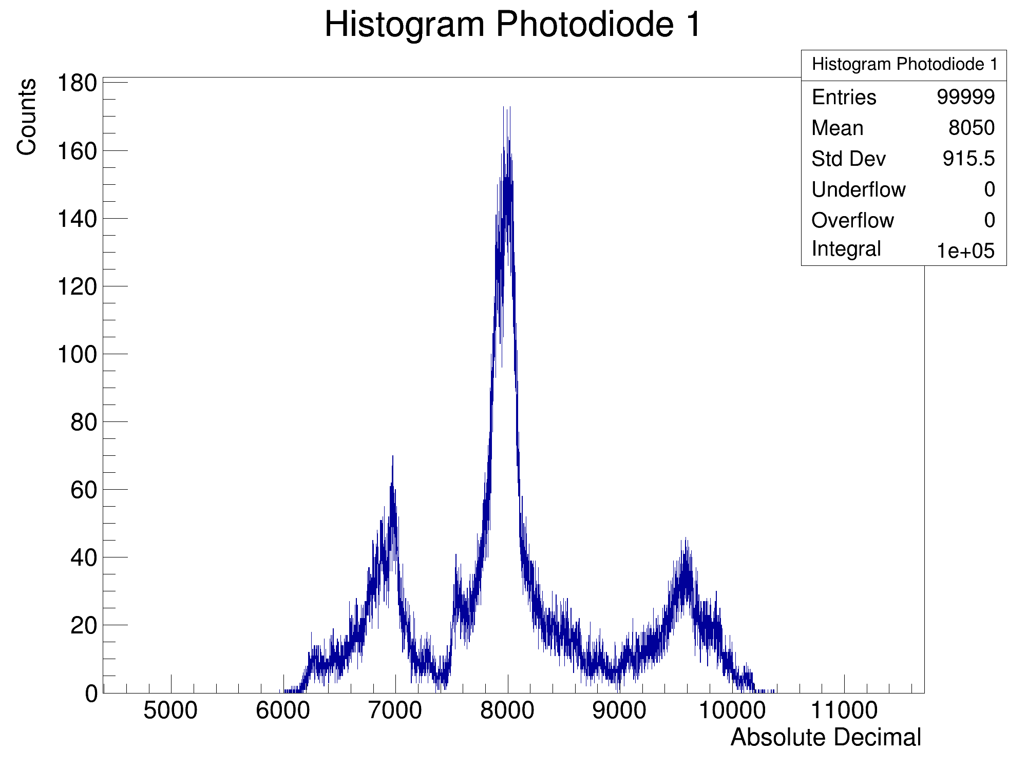
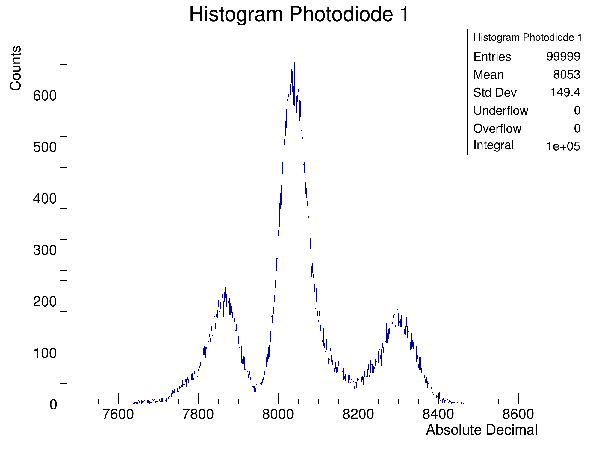
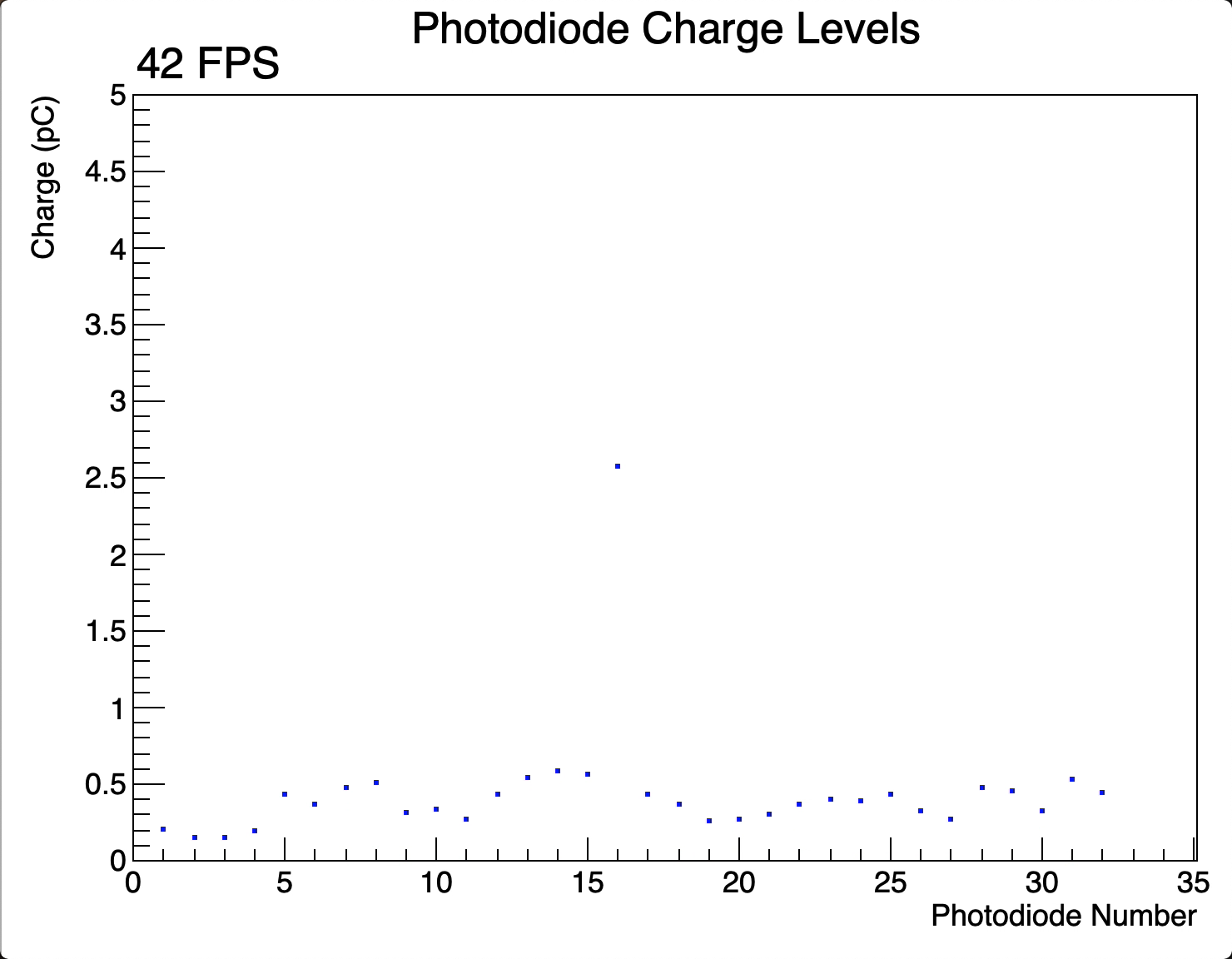
|14 || | |14 || D27, CMOS off, 12.5pC, grounded, LED. LED pulse of 1MHz, 6V height and 500ns width. Injected into single scintillator sheet coupled to photodiode 16. || | ||
<div class="image150px" style="text-align: center;"> | |||
[http://www.hep.ucl.ac.uk/pbt/wikiData/movies/DDC232/210422/Histograms/Run014.png http://www.hep.ucl.ac.uk/pbt/wikiData/movies/DDC232/210422/Histograms/Run014.png] | |||
</div> | |||
|| <div class="image150px" style="text-align: center;"> | |||
[http://www.hep.ucl.ac.uk/pbt/wikiData/movies/DDC232/210422/Run014.mp4 http://www.hep.ucl.ac.uk/pbt/wikiData/movies/DDC232/210422/Thumbnails/Run014.png]</div> | [http://www.hep.ucl.ac.uk/pbt/wikiData/movies/DDC232/210422/Run014.mp4 http://www.hep.ucl.ac.uk/pbt/wikiData/movies/DDC232/210422/Thumbnails/Run014.png]</div> | ||
|- | |- | ||
Latest revision as of 09:54, 29 April 2021
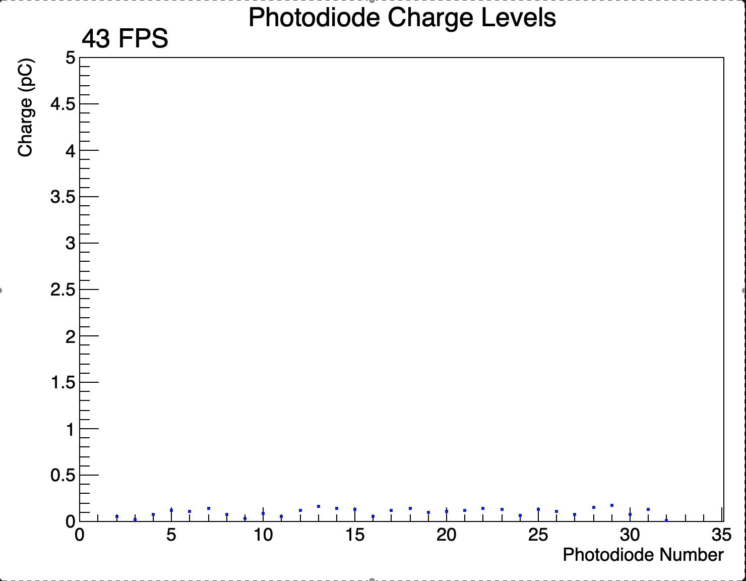
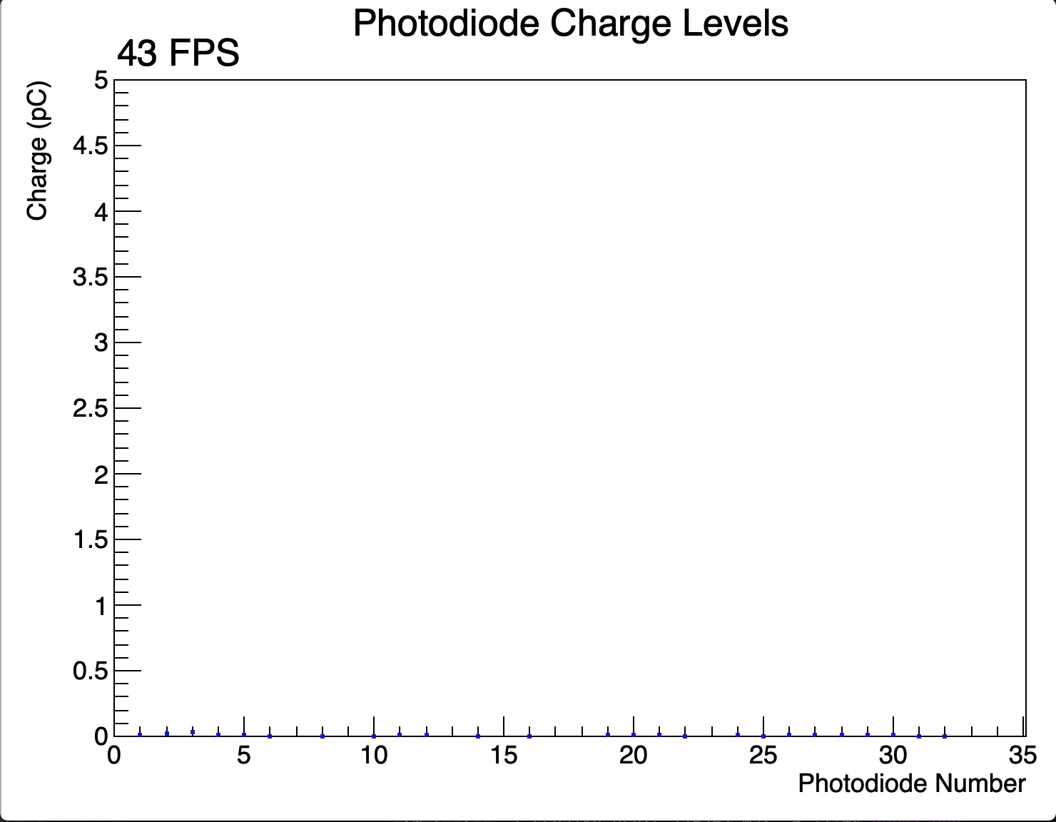
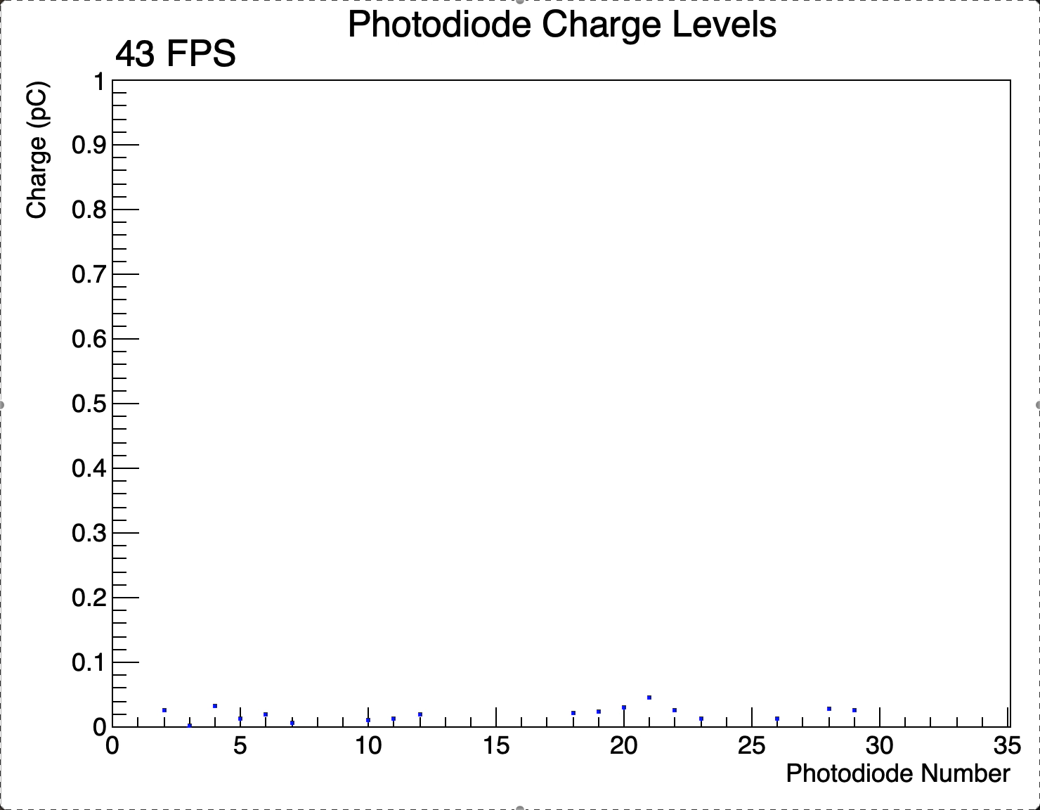
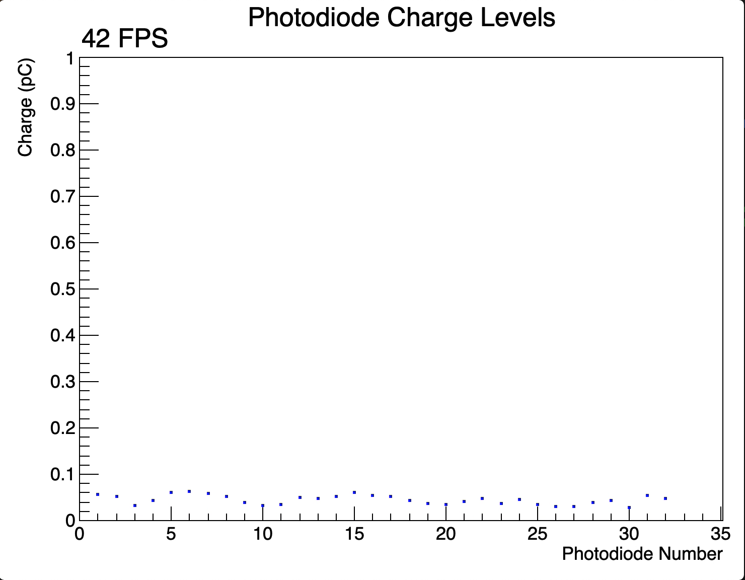
Noise tests of UCLH beam test setup in D109/D27.
Aim: Investigate source of external electronic noise observed at UCLH by measuring dark noise in lab/office with CMOS sensor turned off/on.
Notes
- D27 is an electronically noisy lab whereas D109 is a quieter office (though still not a perfectly shielded environment).
- Test 2 DDC232 boards coupled to scintillator stack.
- CMOS sensor coupled to scintillator stack on perpendicular face.
- Both CMOS sensor daughter board and DDC232 Nexys Video board in detector enclosure.
- In all runs, an integration time of 170us is used.
- Video steps through individual consecutive acquisitions at frame rate shown. Each frame represents 170us in time.
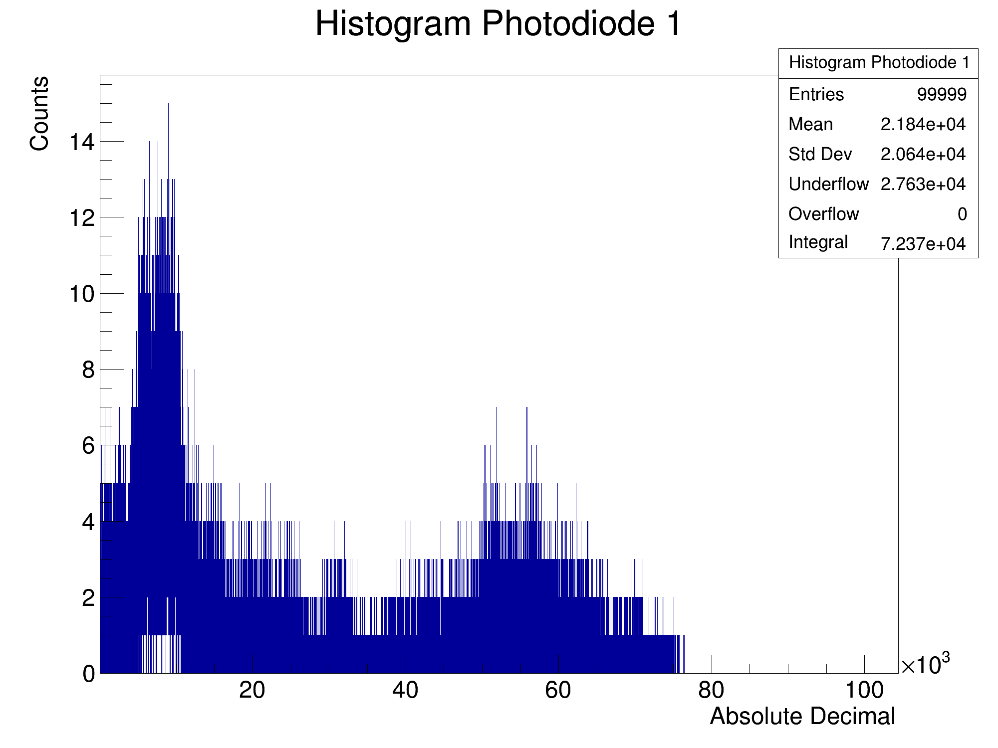
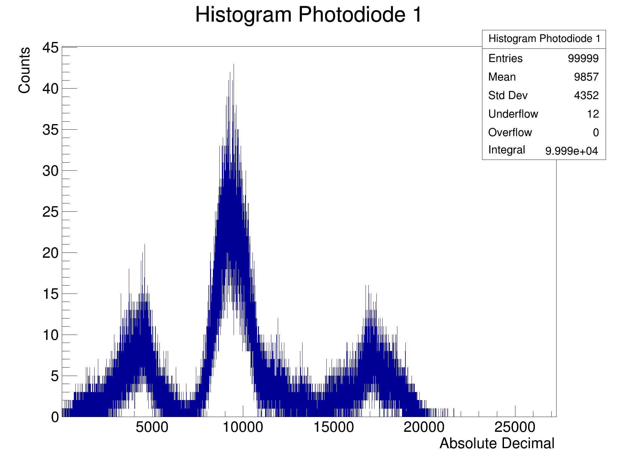
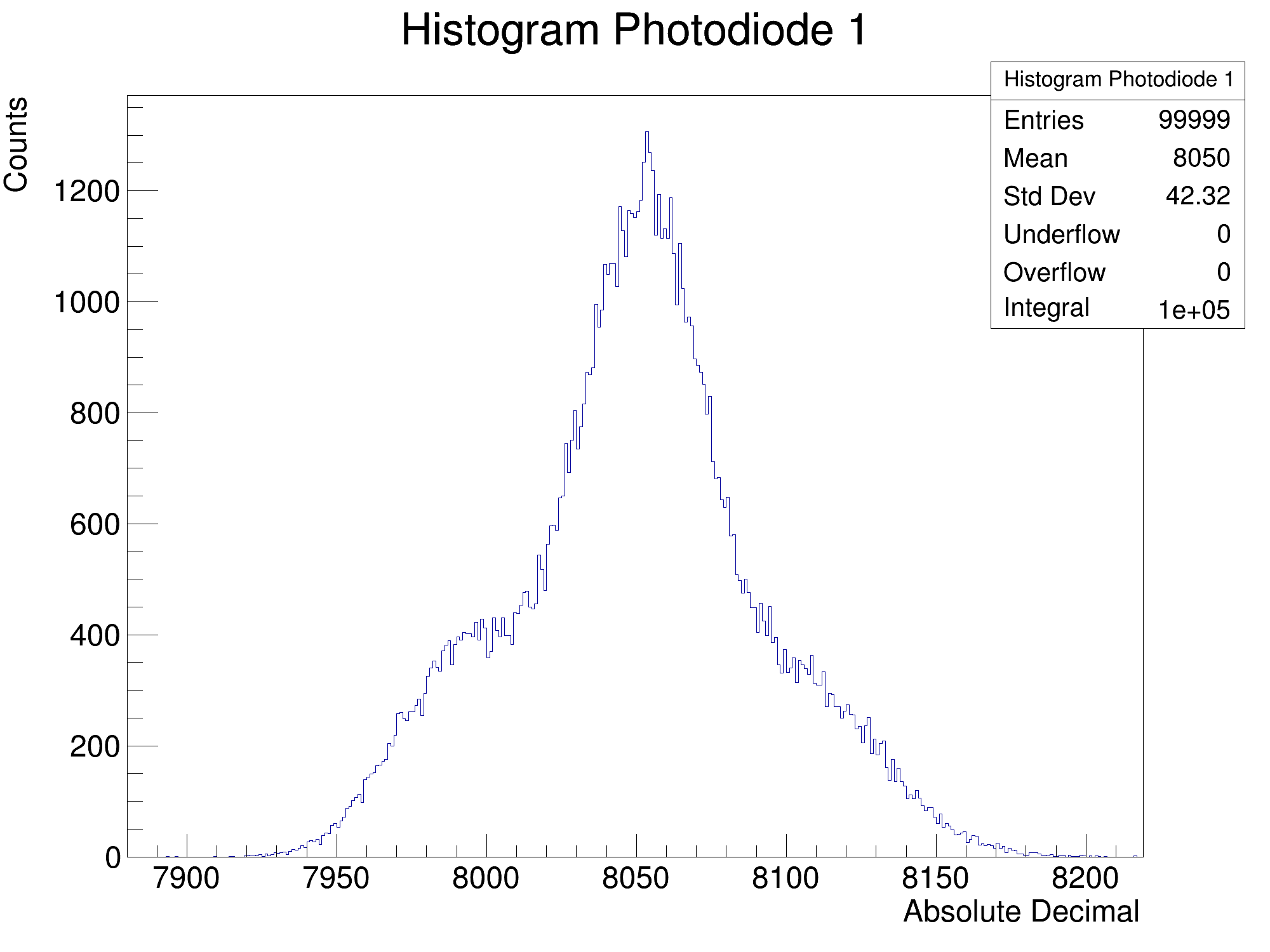
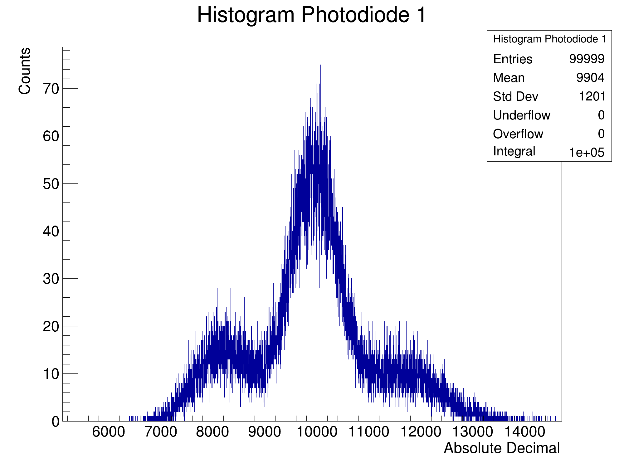
- Histogram of one photodiode also provided. Expect to see clean gaussian shape if no external noise is being picked up.
- Signal photodiode shown for Run 14.
- Note the absolute value of the y-scale, which differs in some clips.
Videos and thumbnails saved in /unix/www/html/pbt/wikiData/movies/DDC232/210422
| Run | Description | Histogram | Video |
|---|---|---|---|
| 1 | D27, CMOS on, 350pC |
|
|
| 2 | D27, CMOS on, 12.5pC |
|
|
| 3 | D27, CMOS off, 350pC |
|
 |
| 4 | D27, CMOS off, 12.5pC |
|
 |
| 5 | D109, CMOS on, 350pC |
|
 |
| 6 | D109, CMOS on, 12.5pC |
|
 |
| 7 | D109, CMOS off, 350pC |
|
 |
| 8 | D109, CMOS off, 12.5pC |
|
 |
| 9 | D109, CMOS on, 12.5pC. Detector housing grounded using ground pin of FPGA. Grounded using optical breadboard inside detector. |
|
 |
| 10 | D109, CMOS on, 12.5pC. Previous grounding seemed ineffective. Now grounded by attaching clip to metal on outside face of detector enclosure. |
|
 |
| 11 | D109, CMOS off, 12.5pC, grounded. |
|
 |
| 12 | D27, CMOS off, 12.5pC, grounded. |
|
 |
| 13 | D27, CMOS off, 12.5pC |
|
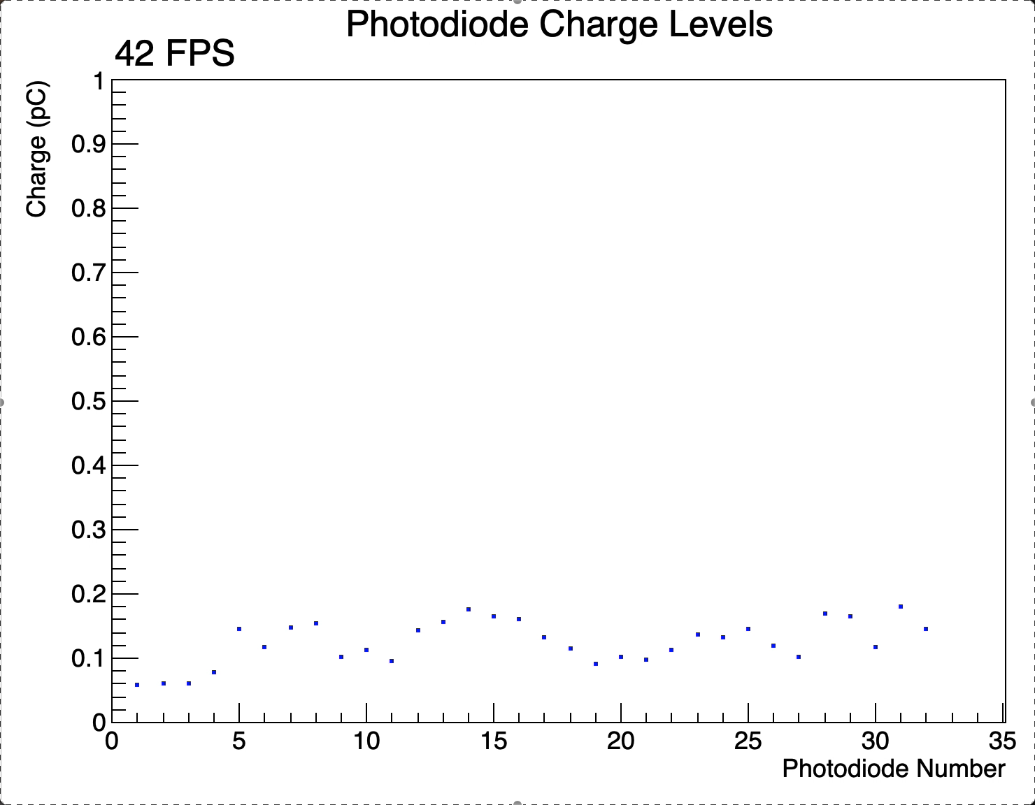 |
| 14 | D27, CMOS off, 12.5pC, grounded, LED. LED pulse of 1MHz, 6V height and 500ns width. Injected into single scintillator sheet coupled to photodiode 16. |
|
 |