

|
|
|
Abstract
An intra-pulse Interaction Point fast feedback system (IPFB) has been designed for the Next Linear Collider (NLC), to correct relative beam-beam misalignments at the Interaction Point (IP). This system will utilise the large beam-beam kick that results from the beam-beam interaction and apply a rapid correction to the beam misalignment at the IP within a single bunch train. A detailed examination of the IPFB system is given, including a discussion of the necessary electronics, and the results of extensive simulations based on the IPFB concept for fast beam correction are presented. A recovery of the nominal luminosity of the NLC is predicted well within the NLC bunch train of 266 ns.
The FONT experiment — Feedback On Nanosecond Timescales — was proposed as a direct test of the IPFB concept and was realised at the NLC Test Accelerator at SLAC. As part of FONT, a novel X-band BPM was designed and tested at the NLCTA. The results of these tests with the NLCTA short and long-pulse beam are presented, demonstrating a linear response to the position of the 180 ns long-pulse beam: measurements show a time constant of ~1.5 ns and a precision of better than 20 μm. A novel BPM processor for use at X-band, making use of the difference-over-sum processing technique, is also presented in detail, with results given for both short and long-pulse beams.
The FONT design concepts and modification of the IPFB system for use at the NLCTA are described. The design of a fast charge normalisation circuit, to process the difference and sum signals produced by the BPM processor, forming part of the FONT feedback circuit, is detailed extensively. Bench tests of the feedback electronics demonstrate the effectiveness of the normalisation and feedback stages, for which a signal latency of 11 ns was measured. These bench tests also show the correct operation of the normalisation and feedback principles. Finally, the results of a full beam test of the FONT system are presented, during which a system latency of 70 ns was measured. These rigorous tests establish the soundness of the IPFB scheme and show correction of a mis-steered bunch train within the full NLCTA pulse length of 180 ns.
“Any intelligent man needs to maintain his intelligence. Intelligence isn't a static property, its dynamic, permanently increasing, yes, but also shifting, moving, sliding, jumping and sometimes leaping into different planes, dimensions, boxes and tunnels. You can't catch it, you can't quantify it, you can't qualify it, you can't see it and you can't understand it. All you can do is feed it, and if it doesn't like the food then give it something tougher to chew on …”
Simon James, MMII
ME SAY NOW. A surprisingly large number of people have participated in the formulation of the work contained within this thesis, without many of whom it is unlikely that much of it would have seen the light of day. As such I have the pleasure of thanking all those who have made this research possible. I must first extend both my thanks and admiration to an outstanding group of physicists at SLAC. Firstly, to Marc Ross, Tonee Smith, Doug McCormick, Keith Jobe, Chris Adolphsen and Janice Nelson who gave an unwarranted quantity of their valuable time and expertise in helping FONT find such success at the NLCTA, and to Dave Brown, Mike Brown and Bill Roster for making most of the important bits work in the first place. My thanks also go to Dave Burke, Tom Markiewicz, Marty Breidenbach, Peter Tenenbaum and Tor Raubenheimer for their help in various aspects of FONT, and Glen White for his simulation work and the various stolen plots that appear throughout this thesis.
I am particularly grateful to Steve Smith for his expertise in the intricacies of beam position monitors and fast feedback systems, and for having the patience to explain them all to me whenever I turned up on his office doorstep. To Joe Frisch, an accelerator physicist of astonishing skill and knowledge, I am indebted for his invaluable help in virtually every aspect of my research, without whom it is unlikely FONT would have achieved anything close to the success we experienced. Another expert whose input was of enormous value is Colin Perry, master of the dark arts of analogue and tube electronics, and with whom I had the pleasure of sharing the bewildered euphoria that everything had actually worked …
For services above and beyond the call of duty, my thanks go to Gavin Nesom, who braved the world of FONT while he had better things to do, argued with me till we were both blue in the face and applied himself with a quiet diligence while all hell was breaking loose in the NLCTA control room. Finally I must thank my two supervisors: Phil Burrows, who fought my corner when no-one else would in engineering my PhD transfer, provided superlative guidance throughout my research and under whom my abilities as a physicist have benefited immeasurably; and Adrian McKemey, who provided a young student with more inspiration than he will ever know.
Lastly, my thanks go to Rich Sloane, Paul Jackson and Ed Hill for keeping me sane in California; Rich Steward, Claire Gwenlan, Chris Smith and Ed Moyse for showing me the light; Keith Hamilton, Thilo Pauly and Mike Ramage for their patient assistance with particle theory; the UCL HEP group for providing me with a home away from home in the early days; various assorted Monkees for keeping me in my place; Nick, Neil and Stuart for surviving the Stoke; Jason Johal and Tom Lyford for making Brunel a brighter place to be; and Liz, AJ and MJ for just being great.
It could be argued that particle physics is currently languishing in one of its least interesting periods since the inception of quantum mechanics at the turn of the 20th Century. As a discipline that thrives on the discovery of new particles to advance both the theoretical and conceptual understanding of its many intricacies and complexities, not since the discovery of the bottom quark in 1977 [1] has particle physics been pushed forward by the appearance of an unexpected new particle1. Although the recent progress made in the measurement of neutrino oscillations points strongly towards physics beyond the Standard Model, very little experimental evidence exists that can be used to guide the creation of theories that properly describe this physics. The many varied theories that exist under the banners of the Higgs Sector, Supersymmetry or “Grand Unified Theories” (GUT's) predict an enormous cornucopia of particles that could exist at energies that have yet to be reached by modern particle accelerators.
|
|
|
|||||||||||||||||||||||||||||||||||||||||||||||||||||||||||||||
|
|||||||||||||||||||||||||||||||||||||||||||||||||||||||||||||||||
The current Standard Model of particle physics is an impressively robust theory. A result of almost a century's observation and refinement, it encompasses virtually every observation that has been made in the field of particle physics. The myriad of bound states, decay products and interaction cross sections are all accounted for within the Standard Model: the resulting particle coupling and decay calculations based upon the Standard Model are some of the most accurate known to man. In the Standard Model, all matter is made from two types of elementary particle: quarks and leptons. The interactions between these fundamental particles are mediated by a third group of particles — the mediators — which are themselves subdivided by force: the photon (γ) for the electromagnetic force, the W+, the W− and the Z0 for the weak force and eight gluons (g) for the strong force2. All the fundamental particles of the Standard Model are summarised in Table 1.1 [2].
The basis of the Standard Model is the underlying symmetry group SU(3)c×SU(2)L×U(1)Y: the SU(3) group describes the strong force while the electromagnetic and weak forces are unified into a single force under the SU(2)×U(1) group [3]. The unification of the electroweak sector, by Glashow, Weinberg and Salam (the GWS model) provided an explanation for the charged weak interactions, via W± exchange, and successfully predicted their masses, along with the existence and mass of the Z0. However, in unifying the weak and electromagnetic forces, it is no longer possible to maintain the exact symmetry of SU(2)×U(1): nature spontaneously breaks this symmetry and the W± and Z0 gain a mass, while the photon remains massless. To account for this electroweak symmetry breaking, something extra must be introduced: the Higgs boson.
To account for the spontaneous symmetry breaking in the electroweak sector, a Higgs field is introduced into the Standard Model Lagrangian [4]. The ‘residue’ of this Higgs field, according to the basic Higgs theory, is a single scalar boson, known as the Higgs boson. It is the manifestation of this Higgs field, and the consequent appearance of the Higgs boson, that is predicted to be the cause of electroweak symmetry breaking [4]. The resultant hypothesis is therefore that the Higgs field is the cause of all the fundamental particle masses and that the Higgs couples to all massive particles, with a coupling strength that is dependent upon the particle's rest mass [1].
| Figure 1.1: The narrowing of the allowed mass range for the Standard Model Higgs boson as a result of precision electroweak measurements at LEP, SLD and the Tevatron (the yellow region shows the upper and lower 95% confidence limits) [5]. |
The Higgs has so far escaped detection, although this is not for lack of trying: data from the last run of the Large Electron Positron collider (LEP) at CERN gave a possible indication of a Higgs with a mass around 114 GeV [5]. However, while the Higgs has not yet been found, measurements with current accelerators do give an indication as to the most likely mass range of the Standard Model Higgs: this is shown in Fig. 1.1. If and when the Higgs is finally found, the probing of the properties of this elusive particle will be essential in the creation of theories that lie beyond the Standard Model. Part of this reshaping of the current landscape of particle physics requires the investigation of physics at the current high energy frontier: it is at these TeV energies that vital experimental evidence for physics beyond the Standard Model will be most forthcoming.
Theories abound as to what lies beyond the predictions of the Standard Model and the Higgs sector. However the candidate that is currently favoured is the concept of Supersymmetry (SUSY). Supersymmetry is based on the idea that every fundamental fermion has a bosonic “superpartner” and vice versa [4]. The superparticles (or ‘sparticles’) have properties that would ideally differ from their Standard Model partners only for the particle's spin. However, this symmetry is clearly inexact, since none of the particles predicted by supersymmetry have been seen. The cause of this discrepancy is similar to electroweak symmetry breaking: the particles and sparticles begin with identical masses and nature spontaneously breaks the symmetry between the two. This results in the sparticles having much larger masses — a necessary condition since none have yet been found. SUSY therefore makes a number of distinct, testable predictions as to the existence of particles outside the Standard Model: in addition to the large number of sparticles, SUSY theories propose the existence of a number of Higgs particles (2 charged and 3 neutral) [6]. The predictions of the cornucopia of supersymmetric theories have yet to be confirmed, but are likely to come under a great deal of scrutiny with the next generation of particle colliders (see Section 1.2)3.
Extensions to this Minimal Supersymmetric Standard Model (MSSM) are varied and provide a number of benefits over the Standard Model. One possibility is the unification of gravity into the forces currently covered by the Standard Model into a Grand Unified Theory (‘GUT’): these place all the forces of nature onto an equal footing, unifying the coupling strengths at a very high energy scale (the so called ‘GUT scale’) [5]. In addition, the various string theories make predictions about the existence of extra dimensions in addition to the appearance of supersymmetry. These theories however will have to wait until more light is shed on physics beyond the Standard Model.
Neutrino oscillations also point the way to new physics. However they are not, of themselves, indicative of physics that truly lies outside the scope of the Standard Model, since it is possible to incorporate these effects into the Standard Model without a great deal of adjustment4. To discover physics that lies beyond the Standard Model, it is essential that particle physics steps beyond the reach of its current tools (the high energy colliders) to attain energies that mean that particle physics can step forward once again into the unknown.
There are a number of ways to investigate the physics that exists outside that encompassed by the Standard Model. It is possible to make precision measurements on some of the predictions of the Higgs sector and non-Standard Model physics with existing accelerator facilities [3]. However, to have direct access to this new physics, new accelerators are required that are capable of reaching these TeV-scale energies. Traditionally (and somewhat erroneously) hadronic machines have been thought of as ‘discovery’ machines, with lepton colliders used as complementary ‘measurement’ machines; the reasons for making such a distinction are given in the next section. However, the choice of beam itself constrains the design of the accelerator: this choice of accelerator design is discussed in the remainder of this chapter.
It is highly likely that the first evidence for any such new physics will be found at either the Tevatron at Fermilab, or almost certainly at the Large Hadron Collider (LHC) at CERN5 [7]. However, neither of these machines will provide the required precision measurements that are needed to test the many postulated extensions to the Standard Model [6]. This is because, unlike LEP — which (as its name would suggest) was designed to collide electrons and positrons — both these accelerators are hadronic: the LHC will use two 7 TeV proton beams, with the Tevatron using 1 TeV proton-antiproton collisions [8]. While these energies are easier to achieve with hadron accelerators (see Section 1.2.2) — making new, high energy discoveries easier as a result — the methods of Higgs production at leptonic and hadronic machines are broadly similar, they are invariably simpler for e+e− collisions [5]. In addition, two features lend themselves extremely favourably to lepton collisions: one is the cleanliness of the interaction and corresponding final state, and the other is the precise initial state energy.
The cleanliness of the lepton interaction is primarily a result of its simplicity, since electrons and positrons are both fundamental point-like particles. In an interaction between the two, there is no “excess baggage”: the collision results in the complete annihilation of both particles and a resultant state with all of the energy of the two colliding leptons and zero net charge. However, in hadronic collisions the interaction occurs between quarks within the composite structure of the hadron, usually via some gluon or W± exchange. Therefore the interaction is both impossible to define prior to the collision and extremely messy: the nature of quark and gluon jets, resulting from the confinement of strongly interacting particles, leads to an enormous number of final state particles compared to lepton collisions, with a good deal more work required to reconstruct the primary vertices of the event.
In addition to the complexity of the interaction, the composite nature of hadrons means that there is no way of precisely defining the energy of each quark prior to collision: only a portion of the total energy of the proton is carried by each quark, so that the resulting interaction does not have a definite initial energy. This is not the case for leptons, since each one carries exactly the same, well-defined energy into the collision. It is therefore possible, with a lepton collider, to precisely vary the energies of the incoming particles and scan the available energy range to measure the energy dependence of particular production cross sections.
A further benefit of e+e− colliders, is the ability to precisely define the helicity of the initial state particles6 and measure the spin dependence of various final states, something that is not possible for hadronic interactions. For these reasons, precision tests of the properties of the Higgs — such as the mass, width, production cross sections, branching ratios and self-coupling — and of the myriad of supersymmetric particles (primarily the light supersymmetric particle, or LSP) are possible only with a lepton collider [9].
There are suggestions that a muon collider, using μ+μ− rather than e+e− beams, would provide the necessary clean interactions while making use of a modified synchrotron design (for more details, see [10]). However, the problems associated with using stable muon beams, primarily related to their short lifetime and consequent beam damping requirements, mean that a muon collider is not currently a feasible prospect. It is therefore necessary to resort to the well-understood tactic of using e+e− collisions, for which a linear collider is required.
The method of charged particle acceleration employed for the two main accelerator designs — the linear accelerator and the synchrotron, or circular accelerator — is essentially identical: this involves the use of accelerating cavities to produce a high voltage gradient through which the particles are accelerated, and is described in detail in Chapter 2. However, there are a number of fundamental differences between the two accelerator types, both of which have their relative merits.
| Figure 1.2: The overall view of the 27 km CERN Large Hadron Collider (LHC), showing the location of the four main experiments: ATLAS, CMS, LHCb and ALICE [11]. |
The synchrotron uses a series of accelerating cavities, arranged in a circle and interspersed with dipole magnets that bend the beam and cause it to travel continuously through a circular orbit [12]. As the accelerated particles become more energetic and their velocity increases, a higher magnetic field is required to bend the particles through the same trajectory. As such, the strength of the bending magnets is adjusted accordingly, to keep the particles on the same orbit. The accelerating field within the cavities is also adjusted so that, as the particles pass more frequently through each cavity, the maximum acceleration is still imparted to the beam; for ultra-relativistic particles the velocity is approximately constant, at the speed of light c, and the RF frequency remains constant. The accelerator currently under construction at CERN is the 27 km LHC which makes use of the circular LEP tunnel, and is shown in Fig. 1.2.
The advantage of using the synchrotron principle is that the same accelerating cavity can be used many times to continuously accelerate the beam, resulting in a certain economy of components. A collider based on the synchrotron design, such as the LHC, will accelerate two beams in opposite directions around the circular trajectory many times, on each occasion increasing the energy of the beam. The beams are then brought into collision at various Interaction Points (IP's) around the circumference of the accelerator: the four experiments at the four IP's of the LHC can be seen in Fig. 1.2. When two beams are brought into collision, the vast majority of particles do not interact at all, but pass through the IP without hindrance. As such, the beam is re-accelerated and re-used many times, before the cumulative effects of the continuous collisions force it to be discarded and the process begun afresh.
| Figure 1.3: An overhead schematic of the Next Linear Collider [13]. The full length of the accelerator at 30 km is larger than the circumference of the LHC. |
The linear accelerator, or linac, is more primitive in concept. The beam is accelerated along a single straight trajectory, from which the accelerator derives its name. The energy of the beam is therefore proportional, for a given accelerating gradient, to the length of the accelerator, since the beam passes only once through each accelerating cavity. Two accelerator paths are required — one for each beam — and the two meet at a single IP7. After passing through the IP, the beam is then discarded into a beam dump, with a new bunch used for each collision. A schematic diagram of the layout of the Next Linear Collider (NLC) — one of the planned next generation linear colliders — is shown in Fig. 1.3.
Although the linear collider seems, at first glance, extremely wasteful in comparison to the synchrotron, there are a number of circumstances in which the performance of the linear accelerator is superior. These relate to a number of shortcomings of the synchrotron: the foremost amongst these is the production of synchrotron radiation. Synchrotron radiation is the emission of EM radiation by any relativistic charged particle that undergoes an acceleration [14]. When the acceleration is in the direction of the particle's motion — such as in an accelerating cavity — the synchrotron radiation emission is negligible. However, when the acceleration is perpendicular to the particle trajectory — such as is applied by the field within the bending magnet of a synchrotron — the energy loss by synchrotron radiation is a significant fraction of the particle energy. This radiation is emitted in a narrow cone that is approximately collinear with the direction of travel of the particle. In addition, the energy loss for a particle deflected through a particular angle scales with the beam energy as E4, strongly influencing the size of the synchrotron required to reach a particular beam energy.
The radiated power due to synchrotron radiation also depends on the rest mass of the radiating particles like 1/m4 [15]. This is the primary reason behind replacing the LEP electron-positron collider with the proton-based LHC, since the energy loss for protons within the same ring is a factor of 1013 smaller than that for electrons at the same energy8. As such, the LEP accelerator — with a beam energy of around 100 GeV within a 27 km ring — represents something of an upper limit in terms of an electron-positron collider that utilises the synchrotron design. As physicists attempt to push to higher energies, it becomes increasingly difficult to replace the enormous power dissipation through synchrotron radiation. A linear collider, however, suffers from no such shortcomings. The beam energy is independent of the particle mass and is dependent only on the number of accelerating cavities (i.e. the length of the accelerator) and the gradient of each cavity.
Another problem with the synchrotron stems from the number of collisions that each bunch has to undergo. The primary goal of any collider is to maximise the Luminosity L. The luminosity is a measure of the number of interactions that occur between particles in the two colliding bunches (and is usually given in units of cm−2s−1) and is defined as:
|
for number of particles per bunch N, number of bunches per train n and machine repetition rate f; HD is the beam pinch enhancement, resulting from the interaction of two oppositely charged bunches (see Section 2.4.3); σx* and σy* are the horizontal and vertical (r.m.s.) beam dimensions at the IP [16]. Clearly, since the luminosity increases for more densely-packed bunches (i.e. smaller beam spot size) and a higher interaction rate (i.e. increasing the frequency of bunch crossings at the IP), the luminosity is maximised by minimising the cross-sectional area of the beam and maximising the frequency with which the bunches are brought into collision. While both types of accelerator can take advantage of more frequent bunch crossings9, a linear collider is able to make use of a much smaller spot size, due to the nature of the beam-beam interaction (see Section 2.4).
Although only a small fraction of the particles within the two colliding bunches actually annihilate to produce new particles, the rest of the bunch does not pass through unaffected. The large EM-fields produced by each bunch, as a result of the large number of charged particles moving at near-light velocities, produce a large force on the opposite bunch. Since a linear collider throws away its bunches post collision, any detrimental effect that the process of collision has on either bunch is irrelevant. A synchrotron, however, must do its utmost to maintain the integrity of each bunch, since each one is recycled and used for multiple collisions. This means that, by squeezing the bunches into a very flat geometry with virtually zero cross-sectional area (and hence increasing the destructive nature of the beam-beam interaction), the linear collider carries a distinct advantage (the full reasons for the selection of such a geometry are given in Section 2.4).
For these reasons it is necessary to construct a linear collider to fully probe the physics that lies outside the reach of the current technology, beyond the Standard Model. A number of technical challenges exist, mainly in the areas of high gradient accelerating cavities and power delivery systems, that must be overcome in order to construct a linear collider capable of delivering the 500 GeV and above collisions required to probe into this new physics. These are described, along with the generic design of the linear collider, in the next chapter.
As mentioned in the previous chapter, higher energy accelerators are required to investigate the TeV energy scale. To complement the new generation of hadronic colliders, a leptonic collider is required, and to accelerate leptons to the required energy, a linear collider is needed. Currently, the highest energy linear accelerator is the SLAC Linear Collider (SLC), which ran from 1989 to 1998 and used 46 GeV electron and positron beams [17]. While the next generation of colliders will use the same principles of operation as the SLC, a large number of improvements are required to reach the required beam energies.
There are a number of different proposed designs for a next generation linear collider, all with the goals of achieving higher energies and luminosities than any of the previous machines. Each design is broadly associated with a particular accelerator laboratory and have the following titles (see the various references for more information):
The TESLA design is unique in that it makes use of superconducting niobium accelerating cavities, whereas each of the other designs uses ‘warm’ (i.e. room temperature) copper cavities; as a result, it also uses a substantially different bunch structure and damping ring design [22]. CLIC is intended as a ‘next-next generation’ accelerator, to take advantage of a number of developments necessary for the other accelerators; it is also the only accelerator to make use of the ‘two-beam’ accelerator concept and is intended to run at the much higher Centre-of-Mass (CMS) energy of 3 TeV [21]. The NLC and JLC, however, are very similar in design, and follow on conceptually from advances made in the design and construction of the SLC. There is also a considerable amount of ‘cross-pollination’ of personnel and technologies between the two collaborations. The remainder of this chapter will describe the generic design of the linear collider, with a focus on the design of the NLC. Some of the design parameters for the initial design of the NLC, and the proposed upgrade (Stages 1 & 2), are shown in Table 2.1 (each of these parameters is explained in the remainder of this chapter).
|
|||||||||||||||||||||||||||||||||||||||||||||||||||||||||
|
An accelerator is made up of a number of discrete sections, each of which accomplishes a different task. A brief overview of these sections is now given: more detail on beam dynamics and acceleration and the interaction region is provided in Sections 2.2-2.4.
Although the bulk of the accelerator is made up of RF cavities to accelerate the charged particles up to the required energies, the front end of the accelerator is dedicated primarily to the production and collection of electrons (or positrons): this section is referred to as the Injector. The basic role of the injector is to produce the high quality particle beam that is to be used for acceleration within the main linac. The electron and positron injectors for the deep-bored-tunnel design of the NLC10 are shown in Fig. 2.1; the figure also shows the general layout of the damping rings: these are dealt with separately in Section 2.1.2. The other components that make up the injector are the source, a pre-accelerator, bunch compressors and various collimation systems [13].
| Figure 2.1: The electron and positron injector complexes for the deep-bored-tunnel design of the NLC [13]. The abbreviations used are as follows: SRCS – electron sources; BC-1 – 1st stage bunch compressor; LTR – Linac-to-Ring; PDR – Pre-Damping Ring; MDR – Main Damping Ring; dimensions are given in metres. |
The source, as its name would suggest, is the first stage in creating a usable particle beam. There are two main ways to create the large quantity of electrons that are required for both the electron and positron source, based on thermionic and photoelectric emission [23]. A high voltage DC thermionic gun uses a heated cathode to produce electrons, which are then initially accelerated with a DC voltage. A series of solenoids is then used to constrain these electrons and compensate for the natural tendency of the trajectories of similarly charged particles to diverge (an effect referred to as ‘space charge’), which would result in a rapid increase in beam spot size [24].
The electron source for the NLC actually makes use of the second method of electron emission: the photoelectric effect. A laser is directed onto a Gallium-Arsenide semiconductor photocathode: the photoelectrons produced are then accelerated in the same fashion as before. This method of electron production allows the selection of the polarisation of the resultant electron beam. Since one is able to choose the polarisation of the photons in the laser beam, the resultant emitted photoelectrons are also polarised, resulting in an electron beam with better than 80% polarisation [6]. A pre-accelerator is then used to further accelerate the beam, with successively higher frequency accelerating cavities (for more details, see Section 2.3). This causes the beam to bunch at the desired bunch spacing — in the case of the NLC, a pair of 714 MHz bunchers is used, setting the bunch spacing at 1.4 ns: the full bunch train consists of 192 bunches of 8×10⁹ electrons, with a full train length of 266 ns. An S-band accelerator, at 2856 MHz, is then used to further accelerate the beam to 2 GeV for injection into the main damping ring (see Fig. 2.1).
A second electron gun is used to produce the electrons that are required to create the positrons for the opposing beam. 6 GeV electrons are accelerated onto a Tungsten-Rhenium (WRe) target, causing electromagnetic showers within the target: the positrons produced by these showers are then collected and accelerated by an L-band linac (1428 MHz) to 1.98 GeV for injection into the positron pre-damping ring [13].
While it is undoubtedly important to produce bunches with a large number of particles, it is perhaps the size of these bunches that is the dominating factor in producing a high luminosity. For a linear collider, the luminosity, L, is defined as:
| (2.1) |
for beam energy E, number of particles per bunch N, number of bunches per train n, machine repetition rate f and beam power P [18]. HD is the beam pinch enhancement, resulting from the interaction of two oppositely charged bunches (see Section 2.4.3); σx* and σy* are the horizontal and vertical (r.m.s.) beam dimensions at the IP11. As such, since the luminosity is inversely proportional to the CMS energy (2E), it is imperative that the luminosity loss caused by going to higher energies is countered by a corresponding decrease in the spot size at the IP.
| Figure 2.2: A transverse phase space plot for a large number of particles in a particle beam [25]. The area of this phase space plot is defined as the (horizontal) emittance of the beam, εx; β is the beta function and is defined in Section 2.2.2. |
In order to produce a minimum spot size, it is necessary to minimise the horizontal and vertical emittance of the beam. The emittance is a measure of both the physical transverse size of the beam, x, and its divergence i.e. the angle12 of each particle trajectory within the beam, x′. If one plots the position versus angle of every particle within the beam, as shown in Fig. 2.2, this forms an ellipse in transverse phase space. The area of this ellipse is defined as the emittance of the beam: it is denoted by
| Figure 2.3: The electron Main Damping Ring (MDR) for the NLC [18]. |
It is the task of the damping rings to produce a beam that is in an optimum condition for acceleration and collision by vastly reducing the transverse beam emittance. This is achieved by making use of the same synchrotron energy loss process described in Section 1.2.3. The electron main damping ring for the NLC is shown in Fig. 2.3. The electron beam is injected into the damping ring and circulated many times: each time it circulates it undergoes the alternate processes of acceleration and energy loss through synchrotron radiation. When the beam passes around either of the two arcs in the damping ring, the curved trajectory causes synchrotron radiation to be emitted, reducing the energy of the electrons. The beam then passes through a series of accelerating cavities which reaccelerate the beam. The emittance reduction occurs because the electrons lose energy in their current direction of travel, but are accelerated only in the longitudinal direction i.e. they lose energy in 3 dimensions and gain energy in 1. This helps to narrow the trajectories of the electrons within the beam until they all lie in approximately the same direction, hence reducing the emittance.
In addition to the energy loss within the two damping ring arcs, a wiggler is used in one of the straight sections to further increase the synchrotron radiation energy loss. A wiggler consists of a series of dipole magnets: the alternating magnetic field, caused by the alternating dipole arrangement within the wiggler, causes the beam to undulate in its trajectory [26]. As the beam undulates it also emits synchrotron radiation in the direction of particle motion, increasing the damping rate per revolution within the damping ring13.
For the NLC, the normalised emittance upon extraction for the damping rings must be reduced to
The bulk of the NLC is made up of the main accelerator tunnel, also referred to as the main linac (see Fig. 1.3). The main linac is used to accelerate the two beams from the post-injector energy of 8 GeV up to the collision energy of 250 GeV (500 GeV for the intended upgrade — see Table 2.1). It is 12.3 km long and consists of 26 sectors, each 468 m long [13]. To reach the intended CMS energy of 500 GeV, only half the linac will be filled with accelerating structures: the other half would be filled for the 1 TeV upgrade. Each sector is split into 9 discrete RF distribution units, each of which contains 8 klystrons and 8 groups of 6 0.9 m accelerating structures [13] — more information on the nature of these structures, and the power delivery systems used to drive them, is given in Section 2.3.
| Figure 2.4: A schematic diagram of the 1996 layout of the NLC beam delivery system [18]; dimensions, except where marked, are given in metres. |
At the end of each of the linacs is the beam delivery system. The purpose of the beam delivery system is to prepare the beams from the linacs, that have now been accelerated to the correct energies, for collision. The role of the beam delivery system is essentially to ensure that the two beams arrive at the IP with the correct spot size. The full NLC beam delivery system consists of a collimation system, the beam switchyard, the final focus, the interaction region (IR) and the beam extraction lines and beam dumps [6]; the beam delivery system is shown in Fig. 2.4.
The first stage of the beam delivery system is the collimation section. The purpose of the collimation system is to remove the proportion of the beam halo that would otherwise interfere with the accelerator or, more importantly, the detector and interaction region (see footnote 2). As such, it has the following requirements [28]:
The collimation system is made up of a series of spoilers and absorbers that are used to ‘scrape off’ the unwanted part of the beam halo (as given by the requirements above). The purpose of the spoiler (or primary absorber) is to ‘blow up’ the beam halo by increasing the angular divergence of the portion of the beam that is intercepted. This prevents the rest of the collimator — the absorber (or secondary absorber) — from having to absorb a large amount of the beam halo, and hence dissipate a large amount of power, within a relatively small amount of material close to the beam [18]. The spoiler is usually much thinner than the absorber — less than a single radiation length, as opposed to
While the whole of the beam delivery system, up to the IP, includes collimation of some kind, the bulk of the collimation system is located upstream of the beam switchyard (BSY). The switchyard is used to direct the bunch train from the linac to one of the two IP's (see Fig. 1.3). Following the switchyard is the final focus system. The purpose of the final focus is to squeeze the beams down to the correct geometry at the IP whilst minimising aberrations introduced in the beam optics by the extremely strong focusing elements (see Section 2.2 for further details). More information on the final focus is given in Section 2.2.5.
The non-zero crossing angle at the IP, of some 20 mrad, means that it is not possible to use the same beamline to deliver the beam to and extract it from the IP: as such, two extraction lines are used to transport the spent beams to the beam dumps. The beam dump is required to dissipate up to 20 MW of spent beam power after the beams have collided at the IP. The beam dumps are situated some 166 m downstream of the IP and consist of a large water tank, interleaved with water-cooled copper plates [18].
In addition to the final focus, the NLC makes use of crab cavities to further enhance the luminosity [29]. Crab cavities are essentially RF cavities with a very fast rise time: as each bunch passes through the cavity, an oscillating transverse electric field kicks the head and tail of the bunch in opposite directions, rotating the bunch and aiming it towards the opposite bunch [30]. The result is that, while the bunches are still subject to a crossing-angle, the collision itself occurs as if the bunches had arrived head-on: this means that each bunch views the opposite bunch as having a smaller horizontal spot size and the luminosity is enhanced.
As mentioned in the previous section, the majority of the collider is made up of long straight accelerator sections that are used to accelerate the beams to the required energies. However, for a successful accelerator, it is not enough to merely accelerate the beam. All accelerators have to achieve the steering and confinement of a charged particle beam along a desired trajectory: colliding 2.7 nm beams from a distance of 32 km is not something that can be achieved without external disturbance or correction. A description of the dynamics of charged particle beams within the confines of the accelerator is now given.
While the charge of the electrons (or positrons) within a beam would naturally cause the beam trajectory to diverge, they also provide a method of constraining the beam to a desired trajectory. The method adopted in accelerators is to use various types of magnets interspersed at regular intervals along the accelerator. When a charged particle enters a magnetic field, the particle experiences a force F, that is related to the magnetic field strength B, the charge on the particle q and the particles velocity v:
| (2.2) |
Therefore, a charged particle within a uniform applied magnetic field will follow a circular trajectory. The centripetal force required to provide the necessary acceleration to bend a particle through such a trajectory is:
| (2.3) |
for a particle of momentum p travelling along a circular trajectory with a radius of curvature ρ. Combining with Eq. (2.2) gives:
| (2.4) |
The quantity Bρ is referred to as the magnetic rigidity and provides information on the required magnet strength and layout for a charged particle with a particular momentum [25]. As such, by manipulating the strength and orientation of an applied magnetic field, it is possible to bend a charged particle through a desired trajectory and steer the beam.
The simplest type of magnet, which operates on just this principle, is the dipole. A dipole magnet is usually constructed from a pair of coils, which are placed parallel to one another (for an example of a dipole magnet used in the SLAC linear collider, see Fig. 5.7). The magnetic field arising from the current flowing in the pair of coils is, for identical coil dimensions and current flow, completely uniform and is perpendicular to the plane of the coils. As such, any charged particle passing between the coils will travel through a curved trajectory, given by Eq. (2.4). The field strength of the dipole is usually integrated along the length of the dipole, giving the total amount of field that a particle will encounter, and is given in units of
| Figure 2.5: The magnet pole arrangement for a quadrupole magnet [25]. The blue lines mark the magnet poles (polarity indicated as ‘North’ or ‘South’); the red lines mark the magnetic field lines. The red arrows indicate the force applied to a positively-charged particle beam travelling out of the page: the magnet focuses in x and defocuses in y and is therefore defined as a focusing quadrupole. |
The field produced by a dipole (or series of dipoles), however, will not provide the necessary focusing required to keep a particle beam constrained to a desired orbit. In order to prevent the beam from diverging from this desired orbit, extra focusing is required that will force off-axis particles back onto the desired trajectory: this is achieved with the quadrupole. A quadrupole magnet is constructed from four poles — two ‘North’ and two ‘South’ — which are arranged as shown in Fig. 2.5. By arranging the poles in this manner, the magnetic field increases as a function of the distance from the centre of the magnet, where:
| (2.5) |
For most quadrupoles the horizontal and vertical focusing strengths are of equal magnitude. A quadrupole is usually characterised by the gradient of the quadrupole field, K = dBx/dy = dBy/dx: this quantity is constant and has units of Kilo-Gauss per metre (kGm-1) or Tesla per metre (Tm-1). The magnet strength can also be expressed in terms of the normalised gradient, k, where k = K/Bρ and has units of m-2. As such, this gives rise to a dipole field that varies with distance from the centre of the magnet. The result is that particles that are further off-axis are steered more strongly back towards the centre of the beampipe, giving an overall focusing effect [25].
| Figure 2.6: The quadrupole arrangement used to construct a FODO cell (adapted from [25]): alternate focusing and defocusing quadrupoles are separated by drift spaces. |
However, due to the arrangement of the field within the magnet, a quadrupole can only focus the beam in one transverse plane at a time: in the other plane, the beam is actually steered away from the ideal trajectory and becomes defocused. A quadrupole that is oriented such that it focuses in x (and defocuses in y) is referred to as a focusing quadrupole, QF, while a quadrupole that focuses in y (and defocuses in x) is referred to as a defocusing quadrupole, QD. To accommodate for the defocusing behaviour of the magnet, quadrupoles are arranged in pairs, as depicted in Fig. 2.6: this magnet arrangement alternately focuses and defocuses the beam and is called a FODO cell (for FOcusing and DefOcusing).
Accelerators are made up of these FODO cells or something similar but more complex. The arrangement of these magnets, and the effect they have on the beam, is similar to the focusing and defocusing effect of lenses in optics: in fact, the treatment of beams within accelerators is similar to that in geometric optics; more information is given in Section 2.2.3. The result of organising the quadrupoles into such a FODO lattice is to cause the beam trajectories to oscillate around the ideal trajectory (usually the magnetic centre of the accelerator beamline components). These oscillations are referred to as betatron oscillations and are a well-defined function of the spacing and focusing strength of the quadrupoles [31]; more detail is given in the next section. These betatron oscillations confine the particles within the beam to a desired range of trajectories by focusing particles more strongly as they stray further from the ideal orbit.
As mentioned in the previous section, betatron oscillations arise as a result of the FODO lattice arrangement within an accelerator. These transverse oscillations are periodic and follow the standard laws for simple harmonic motion. For oscillations within a FODO lattice, of magnitude x, the general equation (known as Hill's equation) for transverse motion within an accelerator is:
| (2.6) |
where s is the longitudinal distance along the accelerator and K(s) is the restoring force due to the quadrupoles; this restoring force is a function of longitudinal position [25]. It can be shown that solutions of this equation for transverse motion within an accelerator have the form:
| (2.7) |
where εx is the horizontal beam emittance, as defined in Section 2.1.2; φx is the initial phase and is also constant [32]. The two remaining quantities, &betax(s) and ψx(s), are both functions of longitudinal position: &beta(s) is the beta function and describes the amplitude modulation of the transverse beam motion; ψ(s) is the phase advance and describes the change in beta phase; both are dependent on the focusing strength of the quadrupoles [31]. There is a second, identical equation for vertical motion: this is assumed in all the following equations and only the version for x is given. The phase advance is related to the beta function by:
| (2.8) |
As such, the rate of change of transverse position, i.e. the angle, x′, is given by:
| (2.9) |
where
| &epsilon = γ(s)x(s)2 + 2α(s)x(s)x′(s) + β(s)x′(s)2 | (2.10) |
where γ(s) = 1+α2/β [32]. This quantity is invariant under a change of s and, therefore, the beam emittance is a fixed quantity for any periodic accelerator lattice. It is also necessary to define the relative phase advance, μ, where μ(Δs) = Δψ(s). The functions α(s), β(s), μ(Δs) and γ(s) are known as Twiss parameters: there are two of each function — one for each transverse plane — and they are used to characterise the accelerator lattice [31].
In order to construct the quantities described in the previous section, a matrix approach is adopted. While the two beta functions — βx and βy — are continuously varying functions of s, the accelerator itself is not: it is constructed from a number of distinct units e.g. a drift section, a quadrupole, a dipole and so on. As such, it is possible to calculate the various Twiss parameters by using a series of matrices to describe each of the discrete elements from which the accelerator is constructed. For the two horizontal beam parameters, x and x′, the translation between two points along the accelerator, s1 and s2, is given by the following matrix equation:
| (2.11) |
where the subscripts indicate the various parameters at the two points along the beamline [32]. In practice, a 6×6 matrix, referred to as the R matrix, is used:
| (2.12) |
where, in addition to the four transverse beam parameters, l is the longitudinal particle location along the length of a bunch and δ is the relative momentum deviation from the reference particle [33]. For the majority of accelerator components there is no x-y coupling and, if all components are symmetrical about y = 0, the R-matrix reduces to:
| (2.13) |
In order to describe beam motion along the accelerator, a matrix is used to describe each of the beamline components: for example, using just the two transverse beam parameters x and x′, the R-matrix for a drift space is:
| (2.14) |
for a drift space of length L, and the corresponding matrix for a quadrupole magnet is:
| (2.15) |
where l is the length of the quadrupole and k the normalised gradient, as given in Section 2.2.1 [34]. For a thin lens approximation, where
| (2.16) |
where
| (2.17) |
with the usual rules for matrix multiplication followed and the numbers indicating the order in which the elements are encountered between s1 and s6. As such, it is possible to track the motion of the beam through the accelerator, given the initial beam conditions. This matrix approach can also be used to track the evolution of the shape of the beam emittance ellipse (as shown in Fig. 2.2).
The equations given in the previous section allow the motion of ideal particles to be predicted exactly. However, not all particles within a bunch will behave in this well-defined manner: errors in the energy or momentum of individual particles, as opposed to the position/angle error that the FODO lattice is designed to counteract, can also lead to significant beam losses. Errors arise in the particle energy/momentum as a result of many effects, such as scattering from gas molecules during the acceleration process or the emission of synchrotron radiation, as well as any energy error introduced at injection. This results in a spread in the momentum of the particles within a beam, Δp/p.
The result of such a momentum error is that the magnetic rigidity, Bρ, changes, in accordance with Eq. (2.4), and hence the bending radius of any dipole magnet; this effect is called Dispersion [25]. As such, in regions of non-zero dispersion a beam will experience an increase in transverse beam size due to the momentum spread in the beam, as a result of the momentum dependence of Bρ. The transverse displacement, Δx, due to the momentum spread is given by:
| (2.18) |
where D(s) is called the Dispersion function. This dispersion function can be calculated from the lattice in the same way as the beta functions and is computed independently for x and y.
In addition to the dispersion, the momentum spread also causes a change in the focusing strength, and hence the focal length, of the quadrupoles, as a result of the change in magnetic rigidity: this effect is referred to as Chromaticity, ξ. The chromaticity is defined as the relative change in phase advance that results from the momentum spread:
| (2.19) |
As before, there is a horizontal chromaticity, ξx, and a vertical chromaticity, ξy. Correction of the chromaticity (called chromatic correction) is important, particularly at the IP, where the beta functions become very small (denoted by β* in Table 2.1) and the final doublet (see below) attempts to focus the beam to a point. As a result of the momentum-dependent variation in focal length, a lack of such chromatic correction at the NLC would result in an increase in spot size by two orders of magnitude [6].
| Figure 2.7: The layout of a sextupole magnet (adapted from [34]). The magnetic field lines are shown in blue, with the polarity of the 6 magnet poles indicated; the 12 magnet coils are also marked. |
Correction of the chromaticity is achieved with another, higher-order magnet, called a sextupole. As its name would suggest, the sextupole has 6 magnet poles of alternating polarity: the magnet pole arrangement and resultant B-field can be seen in Fig. 2.7. This pole arrangement gives the following B-field [35]:
| (2.20) |
This means that a particle that passes through the sextupole receives a deflection that is proportional to the square of the horizontal distance from the centre of the sextupole. As such, it behaves like a quadrupole whose focal length is a function of the horizontal distance from the centre15. By placing the sextupole next to a quadrupole in a region of finite dispersion, the transverse beam spread that results from such a dispersive region (see above) allows the sextupole to correct for the chromaticity of the quadrupole. For a quadrupole/sextupole pair, the beam deflection is given by:
| (2.21) |
where Kq is the integrated field strength of the quadrupole, Ks is the integrated field strength of the sextupole, ls is the length of the sextupole, Dx is the horizontal dispersion and δ is the relative momentum error, Δp/p [36]. It is therefore possible, by introducing dispersion in only one plane (the horizontal), to correct for the chromaticity in both planes. In addition to the desired correction, a sextupole will also introduce unwanted nonlinear effects: cancellation of these higher-order terms is covered briefly in the next section.
| Figure 2.8: A schematic diagram of the magnet layout for the chromatic correction section of the NLC Final Focus optics: the quadrupoles are indicated by the lenses (for focusing/defocusing quads), with the sextupoles marked by hexagons. MF,D indicates the transport matrices for sextupole pairs and RF,D the transport matrices to the IP [37]. |
As mentioned in the previous section, chromaticity correction is most important in the final focus section of the beam delivery system (see Section 2.1.3 for details of the complete beam delivery system). The purpose of the final focus is to reduce the beam spot size at the IP to provide the maximum luminosity [29]. This is achieved with a pair of very strongly focusing quadrupoles — one for x and one for y — that are situated close to the IP: these are usually referred to as the Final Doublet (FD). The innermost quadrupole of the final doublet is mounted 4.3 m away from the IP (a distance denoted by L*): the full layout of the NLC final focus is shown in Fig. 2.8.
| Figure 2.9: The horizontal and vertical beta functions (βx, βy) and horizontal dispersion (Dx) for the full NLC Final Focus optics; the magnet layout shown in Fig. 2.8, including the IP, are at the right hand end, at ~650 m [13]. |
The corresponding beta functions for the final focus are shown in Fig. 2.9. The major source of chromaticity at the IP is the two final doublet quads: as such, most of the final focus is geared towards the cancellation of this chromaticity [13]. A pair of quadrupoles is required to focus in both planes and demagnify the beam to a waist at the IP. In order to locally cancel the chromaticity produced by these very strongly focusing magnets, a pair of sextupoles — one for x and one, rotated by 180°, for y — is placed upstream of each of the final doublet quads to apply the necessary chromatic correction. A dipole is then used to create horizontal dispersion in the beam to provide the necessary beam spread for the sextupole correction (see above). In addition, the sextupoles themselves generate higher order geometric abberations: to help cancel these unwanted terms, a second pair of sextupoles is located upstream of the first pair, separated by 180° of beta phase [37]. This arrangement of sextupoles is referred to as the chromatic correction section [29].
The front end of the final focus is referred to as the beta-matching section. The purpose of the beta-matching section, as the name would suggest, is to match the beta functions at the end of the linac to those required by the final focus. In other words, one tracks back from the final doublet, through the chromatic correction sections, tracking the beta functions and phases and attempts to match the beta functions at the start of the chromatic correction section with those that arise at the end of the collimation section (see Fig. 2.4). This is the purpose of the 4 quads situated furthest upstream in Fig. 2.9.
The acceleration of charged particles is in essence relatively simple. In an electric circuit, an electric current in a medium, consisting of a continuous flow of electrons, is created with the application of a potential difference, or voltage. The application of this potential difference gives rise to an electric field within the medium that pulls the electrons along, creating the current.
An almost identical principle is adopted for the acceleration of charged particles within an accelerator. Instead of transporting the electrons (or positrons) through a current-carrying medium, the particles are confined to a beampipe, using the principles described in Section 2.2. However, the key difference is in the application of the accelerating potential. It is no longer possible to apply a static, DC potential between two points to accelerate the electrons (the ‘Van De Graaff’ accelerator), since it is impossible to sustain the enormous E-fields required: an accelerating gradient of many MegaVolts per metre (MVm−1) is necessary to reach the required GeV energies [38]. Instead, time-varying fields are used to accelerate a bunched beam.
It may seem at first glance that using an AC potential to accelerate particles would be completely counterproductive, producing no net accelerating gradient. However, it is the very fact that the time-integrated E-field is zero that allows such high fields, of many MVm−1, to be sustained. The simplest way to apply such a varying potential is the Wideroe scheme, shown in Fig. 2.10.
| Figure 2.10: The Wideroe scheme for charged particle acceleration (adapted from [38]). A time-varying voltage is applied to alternate plates, accelerating the particles between the drift tubes; the voltage is indicated by the arrows. |
The beampipe is divided into sections, with a gap between each: an alternating voltage is applied to the plates in the manner indicated in Fig. 2.10. The applied voltage is at its maximum when the particles reach the gap between these drift tube sections and is zero when the particles are right in the centre of a drift tube. This means that, with the particles in between drift tubes, the previous section repels the particles forward, with the approaching section also attracting the particles forward. This method also has the effect of causing the particles to bunch, since slower (or lower energy) particles will be lost from the back of the bunch, while faster particles will not receive the maximum acceleration and will therefore also move backwards into the bulk of the bunch.
However, the disadvantage of such a scheme is that there is no way to drive lower energy particles with a higher voltage while driving higher energy particles with a lower voltage to longitudinally compress the bunch. In addition, power is radiated from the drift tubes since there is no way of preventing it from being lost, reducing the efficiency of the accelerator. The bunch also only receives a brief acceleration between beampipe sections. The solution to the first two problems is to fully enclose the accelerating gap between the beampipe drift sections in a resonant cavity. The primary benefit is that the energy produced by the voltage source is trapped within the cavity and dissipates only slowly into the walls of the cavity [38].
|
|
|||
| (a) π mode | (b) 2π mode | |||
| Figure 2.11: The π and 2π modes for adjacent single-gap cavities [39]. The width of each cavity is governed by the frequency of the injected RF and the mode utilised; the mode number indicates the phase difference between adjacent cavities. | ||||
Instead of applying a voltage externally to the structure to provide the necessary gradient, the E-field is injected directly into the structure in the form of high frequency RF. The intention is then to make sure that the E-field within the cavities sets up a resonant oscillation: as such, the cavity length is usually designed to be half the wavelength of the injected RF, λ, where
There are two possible modes in which to inject the RF, referred to as the π mode and the 2π mode, both of which are shown in Fig. 2.11. In the π mode (Fig. 2.11(a)) each cavity is out of phase with the adjacent one, whereas in the 2π mode (or 0 mode: Fig. 2.11(b)) each cavity is in phase. This means that, in the 2π mode, the radial walls of the cavity become redundant and it is possible to immerse the whole structure in a single E-field: this is known as an Alvarez linac [38]. For a particular frequency, the π mode allows for a gradient twice as high as the 2π mode and therefore a shorter linac [39].
| Figure 2.12: The accelerating gradient, in the form of the applied E-field, experienced by 5 different particles in an accelerating cavity as a function of the time at which they arrive at the cavity t (adapted from [25]). A is the synchronous particle, B is higher energy, C is lower energy, D is on the edge of stability and E experiences a retarding potential. |
By appropriately selecting the phase (i.e. the timing) of the E-field introduced into the cavity, it is possible to significantly compress the bunches and correct for any longitudinal position or energy error: this is shown in Fig. 2.12. While it may seem that the maximum acceleration is gained by introducing the electron bunch into the cavity in phase with the maximum E-field strength, it is actually more advantageous to introduce the bunch slightly early (particle A). By doing so, any particle that arrives slightly earlier (usually as a result of being slightly too high in energy) will experience a smaller E-field and accelerating force (particle B). Conversely, any particle arriving later (with too low an energy) will receive a greater acceleration (particle C).
This gradient in the energy gain causes the particles to bunch together at the frequency at which the RF is applied (which is often referred to as the bunching frequency) — this clumping region in the RF is called an RF bucket. This includes particles that are very far off in energy: those that arrive much later will receive a negative acceleration (particle E) and be slightly retarded, forcing them back into the bunch behind. They then proceed to undergo the same under-acceleration/over-acceleration process as described above.
|
Figure 2.13: The longitudinal phase space ellipse, in |
As such, the off-energy particles within a bunch actually circle around the central particle (particle A in Fig. 2.12, referred to as the synchronous particle) in energy-position space, forming another phase-space ellipse: as with horizontal and vertical phase space (cf. Section 2.1.2 and Fig. 2.2), the area of this ellipse is referred to as the longitudinal emittance. The boundary of this phase space ellipse is called the separatrix and marks the stable boundary of the particles within a single bunch (particle D in Fig. 2.12): this is shown in Fig. 2.13. The particles within the separatrix undergo the cyclical relative acceleration/deceleration: those outside the separatrix are lost, either to the following bunch or from the accelerator altogether. In this way, particle motion with longitudinal stability and a small energy spread is achieved.
Modern accelerating structures operate on principles similar to those described in Section 2.3.1. However, since electrons of a few hundred MeV are already highly relativistic, it is not necessary to vary the length of the drift spaces within a structure as is usually done with an Alvarez structure. As such, it is possible to shorten the drift spaces a great deal so that the electron bunches spend more time within the accelerating field. Such a structure is called a Standing Wave structure: an example of a standing wave structure for the NLC is shown in Fig. 2.14 [38].
| Figure 2.14: A 15-cell NLC copper standing wave structure, installed at the NLCTA (see Section 5.1 for details of the NLCTA) [40]. The two waveguides feed the RF power into the structure through the centrally-mounted input couplers. |
The RF is introduced into the structure in such a way (i.e. with the correct mode) that a standing wave is set up along the length of the structure, with nodes at the interfaces between the cavities, or cells. The standing wave consists of a longitudinal electric field, with no longitudinal magnetic field (a transverse magnetic, or TMmn mode): this provides the necessary accelerating force in the form of the longitudinal E-field. Such a structure is usually driven in the π mode, with the E-field configuration shown in Fig. 2.11(a) [39]: the size of the cells is designed to be resonant at the accelerating frequency. The structure uses a single pair of centrally-mounted RF input couplers to deliver power into the structure (see Fig. 2.14). This input power is used to sustain the accelerating field within the structure and deposit power to the beam: any unused power either gets absorbed by the structure (hence the copper cooling pipes mounted on the outside of the structure) or escapes down the beampipe.
| Figure 2.15: An NLC travelling wave structure, installed at the NLCTA [40]. The structure has 4 RF couplers: two input and two output. |
A development of the standing wave structure, used almost exclusively in linear accelerators, is the Travelling Wave structure: an NLC travelling wave structure is shown in Fig. 2.15. The method of acceleration is similar to the standing wave structure, in that a time-varying longitudinal E-field is used to accelerate the beam as it passes through the cavity: however, instead of setting up a fixed standing wave (forming nodes of oscillation at the cell boundaries and antinodes in the centre of each cell), the sinusoidal E-field is now launched from the front of the structure and runs along in synchronisation with the beam [39]. As such, the maxima and minima of the accelerating field are no longer fixed (‘standing’) but move with the beam (‘travel’), providing a continuous acceleration.
Instead of behaving as a resonant cavity, the structure now behaves as a waveguide, allowing RF power to travel along its length [38]. Waveguides are essentially tubes, with either a rectangular or circular cross section, that allow the transmission of electromagnetic waves (and hence RF power) with virtually no power loss. The energy is stored and transmitted in the form of resonant electric and magnetic fields within the structure [39]. The available modes of oscillation within the waveguide, for a particular frequency, are fixed by the transverse dimensions of the waveguide: the minimum frequency sustainable within a waveguide is referred to as the cutoff frequency [41].
There are two main types of oscillation: the TEmn, or Transverse Electric modes, where there is no longitudinal E-field, and the TMmn, or Transverse Magnetic modes, which has no longitudinal B-field. In addition, there are also TEM modes with purely transverse fields. The subscript mn indicates the order of the mode, with higher order modes requiring larger resonant cavities16. Clearly, for the purposes of acceleration, a longitudinal E-field is required to accelerate the beam along the beampipe: as such, only TM modes are used within the structure [39]. The RF is injected into the structure at the front and extracted at the rear, hence the doubling of the number of waveguide couplers seen in Fig. 2.15.
The rate of advance of the E-field maxima (the phase velocity, vp) is set by the spacing of the cavities within the structure and should be the same as the particle velocity
In general, travelling wave structures are cheaper to produce for a particular gradient: however, it is possible to achieve higher gradients with a standing wave structure [13,42]. Travelling wave structures are necessarily longer, since it is desirable to use up all the injected RF as it is dissipated along the length of the structure before being extracted. A standing wave structure has no such condition, since all the power is retained within the structure. As such, the shorter standing wave structures can hold a higher gradient: in addition, any breakdown within the cavity will result in a higher power deposition in a travelling wave structure, since the longer structure holds more power [43].
However, both cavity types are required to achieve a higher gradient than is actually needed. This is a result of a phenomenon called beam loading. Beam loading results from the interaction of the beam with the conductive walls of the accelerating structure. As the beam passes through the cavity, the EM-field surrounding the beam interacts with the cavity, producing a wakefield that acts against the accelerating field: this reduces the magnitude of the longitudinal E-field and hence the accelerating gradient. This is similar to the back-EMF produced by an electric motor as a result of its inductance. This gradient reduction occurs gradually along the length of the bunch train, resulting in a smaller gradient for the rear bunches. To compensate for this effect, the RF input power at the NLC is ramped, so that the power reduction that occurs as a result of beam loading matches the power increase supplied by the RF system. As a result, the NLC accelerating structures are required to achieve an unloaded gradient of 70 MV/m, but a loaded gradient of 55 MV/m [13].
Since the size of the cavities, in all dimensions, is dependent upon the RF frequency, higher frequency RF drive is favourable as it provides both a higher gradient and shorter bunches (see Section 2.3.2) for a smaller, cheaper structure: however, higher frequency RF is more difficult (and more expensive) to produce, with correspondingly tighter tolerances required in the manufacture of the structures, further increasing the cost; there is therefore a tradeoff in achieving the cheapest and most beneficial solution. The NLC main linac uses an X-band drive frequency of 11.424 GHz, with copper travelling wave structures [13].
| Figure 2.16: A schematic drawing of an NLC X5011 periodic permanent magnet (PPM) focusing klystron [18]. The drift tube consists of a number of small RF cavities; the ion pumps are required to prevent the electron beam scattering off gas inside the klystron. |
Given the enormous gradients that have to be sustained within the NLC accelerating structures, a correspondingly large amount of power is required to sustain these large E-fields. As such, the delivery of RF power to the structures is a crucial part of the NLC main linac. In order to produce the 50 MW peak powers required by the RF system, a high power RF source called a klystron is used. A schematic diagram of an NLC klystron is shown in Fig. 2.16.
A klystron is almost an accelerator in miniature. An electron gun at the bottom of the klystron creates a burst of electrons. This electron pulse then passes through a resonant bunching cavity: into this cavity is injected a steady RF flow (CW, or Continuous Wave) at the desired accelerating frequency. Since the cavity is also resonant at this frequency, the electron beam becomes strongly bunched at this frequency as it travels out of the cavity. The bunched beam then passes through a second, output cavity that is also resonant at the accelerating frequency. This resonance causes the bunched electron beam to very strongly excite the cavity at the accelerating frequency: the RF produced within the cavity as a result is then coupled out through a waveguide, which carries the amplified RF power out to the structures (see above). The electron beam is then dumped into a beam stop at the top of the klystron [44].
In practice, a number of input and output cavities may be used to maximise both the electron bunching and the amount of RF power that can be extracted from a single klystron. This use of resonant cavities creates a large amplification of the RF signal input to the bunching cavity: gains of 106 are possible with modern pulsed-power klystrons [44]. Two power sources are required to provide the input power to the klystron. The RF input to the bunching cavity is produced by a low-level RF system: this provides the RF ‘input’ signal that is amplified by the klystron and is usually a CW microwave source, such as a travelling wave tube (TWT) [13].
The input power to the klystron is provided, through the electron gun, by a modulator [45]. A modulator is used to produce the pulses that drive the electron gun in the klystron and produce the high intensity electron beam. It is through the modulator pulse that the klystron receives the power that amplifies the low level RF input into a high power output to drive the structures. The modulator pulse is a DC square pulse that lasts for a few microseconds: pulsing the modulator allows for a higher peak output and therefore larger power delivery to the accelerating structures.
The klystrons in the NLC are assembled into groups of 8, referred to as an ‘8-pack’, with each powered by a single 500 kV modulator: these make up a single RF distribution unit, of which there are 9 in each linac sector (see Section 2.1.3). Each klystron 8-pack supplies 8 groups of 6 structures, with power delivered to each group of structures via a pulse compression system called the Delay Line Distribution System (DLDS) [13]. DLDS allows the combination of the 3.2 µs RF pulses produced by each klystron into 8 consecutive 396 ns pulses, which are then delivered to the groups of 6 structures. As such, up to 600 MW of peak power can be delivered to the accelerating structures [13].
The IP is the most important part of the entire accelerator. It is the point at which the electron and positron beams are brought into collision and around which is mounted the detector to measure the decay products resulting from these collisions. The beam-beam interaction in linear colliders is markedly different from that in synchrotron machines, primarily as a result of the extreme beam geometry used in linear colliders. From Section 2.1.2, the luminosity is defined as:
|
with the quantities as defined previously. As one would expect, the collision rate is a function of the temporal and spatial density of the particles brought into collision i.e. the number of particles forced into collision per second (indicated by nN2f) and the transverse size of the beam bunches (governed by the r.m.s. transverse beam sizes at the IP, σx* and σy*).
To counteract the lower bunch crossing frequency, a linear collider uses a considerably smaller beam spot size than a synchrotron. However, this in turn introduces other effects into the beam-beam interaction which do not affect collisions in a synchrotron. Whereas a synchrotron will recycle the beams continuously for minutes or hours at a time, with virtually no ill effects from each bunch crossing, the violence of the beam-beam interaction in a linear collider is considerable: the carefully prepared bunches are virtually torn to pieces by the intensity of the collision. These beam-beam effects can essentially be split into two categories [46]:
The phenomenon of beamstrahlung is closely related to two other well-known phenomena: bremsstrahlung and synchrotron radiation. Both processes involve photon emission by accelerated charged particles. A description of synchrotron radiation is given in Section 1.2.3. Bremsstrahlung, or braking radiation, is the emission of a single photon by a charged particle as it traverses a bulk material and passes through the EM-field surrounding an atom. It is most commonly seen in electromagnetic showers as part of the energy loss process of an energetic particle in a scintillator or absorber.
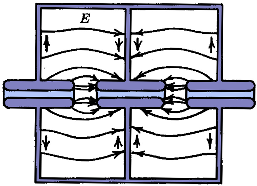
| Figure 2.17: Schematic representation of beamstrahlung emission during the beam-beam collision (adapted from [47]). The trajectory of a single particle in the electron bunch (blue) is indicated by the curved black line: passing through the EM-field of the colliding positron bunch (red) causes it to bend and emit a beamstrahlung photon (green). |
The emission of beamstrahlung occurs not in an absorbing medium, but in the EM-field of a charged bunch. As the two oppositely charged bunches pass through one another, the EM-fields surrounding each bunch cause the trajectories of the particles within the opposing bunch to bend, stimulating the emission of energetic photons: this is illustrated schematically in Fig. 2.17. For bunch dimensions of the NLC, the average EM-field in each bunch during collision is in the kilo-Tesla range [46]: with such large fields, the energy and luminosity loss at the IP can be significant. Not only can beamstrahlung increase the energy spread within the beam, in the same manner as ISR18, but the beamstrahlung photons can also pair produce and cause scattering collisions within the bunch [36]. In addition, if not adequately minimised, energy loss by beamstrahlung can impose an upper limit on the possible CMS collision energies.
The beamstrahlung phenomenon is characterised by the beamstrahlung parameter, Υ, which is a measure of the field seen by a beam particle in its rest frame and is defined as follows [48]:
| (2.22) |
where me is the electron/positron rest mass, q is the electron charge, pμ is the electron four-momentum and Fμν is the mean energy-momentum tensor of the bunch field. The critical magnetic field, Bc, is defined as:
| (2.23) |
giving a mean bunch field for the NLC of ⟨E + B⟩ ≈ 990 Tesla (using the parameters from Table 2.1). During a single collision, the field strength will vary along the length of each bunch. It is possible to define an average and maximum beamstrahlung parameter — for beams with a Gaussian transverse particle density, these are [46]:
| (2.24) |
where re is the classical electron radius, α is the fine structure constant and σz* is the IP r.m.s. bunch length. The two key parameters resulting from beamstrahlung are related to the photon energy loss. The average number of photons radiated during a single bunch collision per electron, nγ, is given by [48]:
| (2.25) |
where λc is the Compton electron wavelength and Υ = Υave. To retain a usable energy spectrum at the IP, nγ should be limited to a value around one [36]. It is also necessary to minimise the amount of energy radiated through beamstrahlung per bunch crossing for the reasons given above. The fractional beamstrahlung energy loss per bunch, δB, is given by [48]:
|
2 |
(2.26) |
with Υ = Υave. Along with the beam size dependence of the beam-beam disruption (see Section 2.4.2 below), it is this dependence of Υ on
In contrast to the quantum nature of beamstrahlung, disruption describes the effect of the classical electromagnetic field surrounding each bunch during the collision and the resulting change in beam trajectories [48]. While the interaction of two charged bunches is a highly complex process, it can be simplified somewhat by making the following assumptions [46]:
For a single particle within a bunch, the equation of motion during collision is given by [46]:
| (2.27) |
with a similar equation for x; here, N is the number of particles in the opposing bunch, nL is the longitudinal bunch density and Φ is the electrostatic potential. Near to the centre of a bunch with a Gaussian transverse particle distribution i.e. where
| (2.28) |
Substituting this expression for Ψ into Eq. (2.27) gives:
| (2.29) |
where y is the transverse beam separation. Assuming that the collisions are approximately head-on
| (2.30) | |||||||||||||||||||||||||
where y0 is the mean bunch separation and
| (2.31) |
The disruption parameter is therefore the ratio of the r.m.s. bunch length to the ‘focal length’ of the bunch. Due to the difference in transverse beam dimensions there is a disruption parameter for each transverse dimension: since the vertical beam spread is much the smaller (and therefore dominant) in linear colliders, Dy is normally quoted. For a uniform longitudinal particle distribution, substituting Eq. (2.31) into Eq. (2.29) gives:
| (2.32) |
during the time that the two bunches are coincident [46]. This equation has solutions of the form sinAt and cosAt, giving rise to sinusoidal oscillations. This essentially means that, as the two bunches pass through one another during collision, they oscillate across one another: this is illustrated in Fig. 2.18. This figure shows the effect of
| Figure 2.18: The effect of the beam-beam interaction on two colliding bunches for D = 40 at discrete time intervals during collision [50]. The left series shows a head-on collision, with the right series showing a slight vertical offset between the two bunches; illustrations are highly schematic. |
The effect of disruption is twofold [49]. Firstly, the mutual attraction of the two bunches causes their trajectories to curve, as given by Eq. (2.30). This curvature, coupled with the oscillations described above and the waist that occurs at the IP, causes a large increase in the angular divergence of the beam as it exits the collision region. Special care must therefore be taken in transporting the beams from the IP to the beam dumps. Secondly, disruption can actually cause an increase in the luminosity, due to the mutual attraction of the two beams: this is particularly effective for a relatively small beam-beam offset, as the attractive force pulls the two beams together upon collision. These are described in more detail in the next section.
Due to the large focusing strength of the final doublet quads, the beam is focused to a very narrow waist at the IP, with
| (2.33) |
The divergence parameter gives a measure of the natural divergence of the beam at the IP (i.e. the IP emittance, εx,y* [48]: a smaller β* results in a larger IP beam divergence due to the focusing force applied to the beam, while a smaller bunch length σz can counteract this divergence by reducing the longitudinal space in which the two bunches interact.
In addition to the hourglass effect, the two colliding beams also undergo a slight compression at the IP as a result of their mutual attraction. This is called the Pinch effect and causes an enhancement in the luminosity, since the beam spot size is reduced by this IP compression. The pinch enhancement factor, HD, gives a measure of the luminosity gain as a result of the pinch effect and is defined as:
| (2.34) |
where L is the measured luminosity and L0 is the nominal luminosity without the pinch enhancement [46]. Due to the complex nature of the beam-beam interaction, there is no precise method of calculating HD; however, it can be approximated by [49]:
| (2.35) |
where only the vertical disruption and divergence parameters are used, since the beam is much smaller in the vertical direction and therefore has much greater vertical disruption. The dependence of HD on Dy is due to the condition of the beams at collision: with a small disruption the beam sees a slight enhancement, increasing the luminosity, as a result of the focusing effect of the beam-beam interaction; with too high a disruption, however, the bunches rapidly fall apart and the luminosity falls off. Determining HD with any degree of precision is only possible with computer simulations [46].
The final effect that results from beam disruption is that of beam-beam deflection. Since the beams are mutually attractive, they will be pulled towards each other when their EM-fields coincide. If the two bunches have a net transverse offset, this attraction will cause the beams to bend round one another, resulting in the curvature of the beam trajectory at the IP.
The deflection curve resulting from this beam-beam kick is essentially a macroscopic version of the force exerted on a single particle from the E-field of the opposite bunch, as described in the previous section (see Section 2.4.2). As such, the outgoing angular distributions are dependent to some extent on the disruption, with the deflection parameter defined as [46]:
| (2.36) |
The outgoing beam deflection angle has the following approximate dependence on ΘD [48]:
| (2.37) |
This phenomenon was observed at the SLC: the beam-beam deflection profile is shown in Fig. 2.19. It was used to measure the beam spot size and to maximise the luminosity by centering the beam at the IP. This behaviour is also predicted to be seen at the NLC. The simulated beam-beam kick for the Stage 1 NLC parameter set (see Table 2.1) is shown in Fig. 2.20. This effect is not a smooth deflection that occurs incrementally over the course of a single collision but rather the cumulative effect of a net transverse beam-beam offset combined with the many transverse bunch oscillations of Eq. (2.32). However, the net effect produces the beam-beam kick of Fig. 2.20.
| Figure 2.19: The measured vertical beam-beam deflection (θye−) as a function of vertical beam offset (Δye+) at the IP of the SLC [51]. The vertical beam size, σy, is approximately 410 nm. |
| Figure 2.20: The simulated beam-beam deflection curve for the NLC [52]. The parameters used are the Stage 1 figures shown in Table 2.1; σy = 2.7 nm. |
This beam-beam kick can actually be used as more than just a diagnostic device that gives information on the beam size. For the beam-beam scans of Fig. 2.19 one artificially produces a relative offset by applying a known deflection to the beam upstream of the IP and measuring the resulting kick. However, maximising the luminosity requires that no such offset is present: if, through random beam motion, the beams become offset at the IP, the luminosity loss is rapid; this is dealt with in more detail in Section 3.1.1. While it is possible to measure the luminosity with dedicated luminosity monitors, these alone do not provide enough information to be able to correct a beam-beam offset.
The beam-beam kick provides a highly accurate method of investigating the relative offset of the two beams. By measuring the position of one of the beams as it leaves the IP it is possible to infer the relative offset of the beams as they collided by making use of the deflection curve of Fig. 2.20. Since the kick is so large, a relative offset of a few nanometres will result in a beam misaligned by hundreds of microns only a few metres downstream of the IP. Even if the absolute position offset (i.e. any offset with respect to, say, the detector) is much larger than the relative position offset, the effect of the beam-beam kick completely dominates the outgoing beam position. This provides a very clean signal on which one can feed back and attempt to correct any beam-beam offset at the IP. A system that attempts such a correction is described in the next chapter.
Maintaining the nanometre-level collisions at the IP is vital to the success of the NLC. While every attempt is made in the accelerator design to maximise the luminosity, through various design refinements mentioned in the previous chapter, a number of factors can lead to significant luminosity degradation, resulting primarily from the vibration of the linac across a large frequency range. Since the vertical beam size at the IP is only 2.7 nm, this places strict tolerances on the vertical motion of the various linac components. To compensate for this luminosity loss, the NLC employs a number of different slow and fast feedback systems. These feedback systems are each designed to address a different cause of luminosity loss and cover a range of frequencies and operating conditions. In addition to the position feedback systems described below, a number of other feedbacks are also utilised to control other features of the beam e.g. beam energy and gun current: for details of these other feedbacks, see [6] and [13]
| Figure 3.1: The simulated luminosity loss as a function of the relative beam offset at the IP of the NLC [52]. |
There are two main causes of luminosity loss, both of which are related to the alignment of the accelerator [13]. The first of these is the relative motion of the two beams at the IP. The luminosity loss as the result of a relative beam offset at the IP is shown in Fig. 3.1: since σy = 2.7 nm for the NLC Stage I, this demonstrates that the accelerator is only 20% productive for a relative beam-beam offset of just 30 nm. The cause of these offsets lies in the transverse motion of the beam, as a result of the dynamic motion of the accelerator components: this random beam motion is referred to as beam jitter. Luminosity degradation also results from an increase in beam emittance caused by misalignments of the accelerating structures. The wakefields created by the passage of a bunch train through a structure (see Section 2.3.3) will apply a transverse kick to each bunch: this kick will cause an increase in the beam spot size which cannot be removed and is called emittance dilution. While both problems have essentially the same root cause, the prevention of emittance dilution will not be dealt with here — for more information see [13].
| Figure 3.2: The power spectrum of ground motion for a number of accelerator tunnels [13]. The 0.15 Hz peak in each trace is due to ocean waves; Hiidenvesi is a cave in Finland used as a reference. |
The primary source of beam jitter is the motion of quadrupoles in the main linac and the beam delivery system: this quadrupole motion accounts for more than half the beam jitter seen at the IP [13]. The main cause of such quadrupole vibration is the natural ground motion of the NLC site (water flow within the NLC structures and amplification of the resulting vibration by the quad supports are also contributory). The power spectrum of the ground motion measured in the SLC accelerator tunnel, as well as a number of other accelerator sites, is shown in Fig. 3.2.
The noise due to ground motion is generally split into two types. Below 1 Hz, the ‘low-frequency’ motion, while of greater magnitude than higher frequency noise, is largely correlated along the length of the linac; above this frequency, the magnitude of the ‘high-frequency’ motion drops rapidly (see Fig. 3.2), but is no longer correlated along the linac. As such, different techniques are required to remedy each type of noise. In addition to this natural ground motion, man-made cultural noise will also cause random accelerator motion: a number of the NLC designs have therefore attempted to site the accelerator away from cultural centres [13].
The primary method of correcting the low-frequency noise is through beam-based steering feedback: this is described in the next section. Reducing the high-frequency motion sensitivity of the accelerator is achieved by careful selection of the NLC site and through optimising the design of the accelerator support structure [6]. Careful design of the RF girders and the quadrupole supports is required to prevent excess vibration, particularly due to man-made sources within the accelerator (such as vibration from cooling systems) to reduce the contribution to the high-frequency jitter.
Beam-based steering feedback is the most commonly utilised position feedback system. It is used to maintain the optimum orbit by adjusting the beam trajectory at various points along the linac. The beam orbit is monitored with a series of beam positions monitors (BPM's — see Section 4.1) mounted inside each of the quads. Pairs of dipole correctors along the linac are then used to actively correct the orbit in response to the position measured by the BPM's. Beam-based steering feedback was originally employed at the SLC as a method of correcting the low-frequency beam motion [53]. The system was a database-oriented design that was used to control a variety of beam parameters, including the beam energy and the beam intensity at the injector. A number of different algorithms were used during the running of the SLC: the database driven design allowed the rapid implementation of new feedback algorithms based on recorded beam data.
A similar system is envisaged for the NLC. With the machine repetition rate of the NLC identical to that of the SLC at 120 Hz, the systems will have similar operating parameters. The Nyquist frequency of such a system is therefore 60 Hz and allows correction of a large quantity of the uncorrelated beam jitter below 60 Hz. Like the SLC, a number of feedback algorithms are under investigation to implement this feedback system at the longer NLC linac [13]. The SLC bunch train, however, was essentially just a single bunch, rather than the 192 bunches of the NLC: as such, this steering feedback system is unable to make the higher frequency 714 MHz bunch-to-bunch corrections. A system capable of such high-speed corrections is detailed in Section 3.2.
While the steering feedback mentioned above is capable of providing sufficient beam stabilisation for frequencies below 1 Hz, it is unlikely to provide a great deal of correction for the high-frequency noise above 1 Hz. While it is possible, through the precise engineering of the beamline supports, to limit the high-frequency motion of the linac quads to less than 10 nm (considered acceptable for the NLC), this is insufficient for the quadrupoles in the final doublet: as such, an additional reduction in the vertical motion of the final doublet by a factor of 2 is required [13].
To reduce the motion of the final doublet, the use of highly compact and rigid permanent magnets would minimise the cooling requirements which could cause excessive vibration. Since the final quads are mounted within the detector, a support structure that is not strongly coupled to the detector is envisaged, to reduce the vibration transmitted through the detector, from ground motion or the detector itself. An optical anchor would then be used to provide rapid feedback on the position variation of the final quad [6].
An inertial stabilisation system for the final doublet has also been proposed, to accommodate the extra stabilisation needed in conjunction with the above construction requirements [54]. The system is designed to actively adjust the position of the final quad to provide the additional vertical stabilisation that is required. The magnet is mounted on active piezoelectric actuators that allow the subtle adjustment of the quad position. A series of piezoelectric accelerometers is then used to measure the movement of the magnet in the frequency range
To supplement both the position feedback and the inertial stabilisation, a beam-based IP feedback system is also required. While the feedback systems described above may provide sufficient luminosity recovery, further reduction of the beam-beam offset can be provided by an intra-train feedback system operating at the IP. The purpose of such a feedback system is to measure the relative beam-beam offset by using the beam-beam deflection and apply a correction within a single bunch train: such a system is described in detail in the remainder of this chapter.
The TESLA design also makes use of an intra-pulse feedback system [55]: however, due to the large differences in bunch structure the NLC requirements for such a system are considerably more challenging. The 950 µs TESLA bunch train consists of 2820 bunches with a 337 ns bunch spacing [5]. Such a large bunch spacing (by NLC standards) allows the implementation of a complex feedback system, based on a digital proportional integral controller, that can correct both position and angle. The TESLA feedback system is essentially divided into 3 stages: the first corrects bunch position and angle at the end of the linac; the second is located in the TESLA chromatic correction section and removes IP angle offsets; and the third is the IP position feedback that makes use of the beam-beam deflection, as described above.
However, since the entire NLC bunch train length of 266 ns is shorter than the TESLA bunch spacing, such a system becomes unusable at the NLC, primarily due to the absolute premium that must be placed on speed of correction. Firstly, the digital electronics used at TESLA are not fast enough to cope with the NLC requirements [56]: it is therefore necessary to resort to analogue electronics to measure the beam position and apply a correction. Secondly, in the TESLA system the correction is applied to the beam by fast kickers with a rise time of 30 ns, which is much too slow for the NLC: this places extra constraints on the NLC power electronics. Thirdly, the system does not have time to make complex corrections based on a large number of measurements: it must be both simpler and more accurate than the TESLA system. As such, intra-pulse feedback for the NLC is a good deal more difficult than for TESLA. The system that has been proposed for the NLC is described in the next section.
A solution for the NLC to the luminosity loss at the IP as a result of inter-train beam jitter was proposed by Daniel Schulte [57]; an improved design with a simplified feedback algorithm was put forward by Steve Smith [58], based upon the Schulte model. The Smith design, incorporating a method for correcting the intra-pulse position jitter, is the one discussed here. The system makes use of the large beam-beam deflection caused by the mutual attraction of the two oppositely charged bunches, as discussed in Section 2.4.3. This beam-beam deflection enhances the relative offset of the beams to such an extent (see Fig. 2.20) that the resulting position offset, some metres downstream of the IP, can be measured with a standard stripline BPM (see Section 4.1 for details of the BPM construction and operation). It is predicted that, with a suitable choice of location for the BPM i.e. far enough from the IP for the offset produced by the beam-beam interaction to dominate, the effect of any absolute position offset at the IP will be negligible [56].
The aim is to make a very rapid measurement of the beam position of the outgoing beam at some point downstream of the IP and, through a certain amount of electronic processing of the measured beam position, redirect the other incoming beam such that the two beams are brought into near-perfect collision at the IP. The key difference between this feedback system and others that are proposed for use within the NLC (see Section 3.1) — and the main reason for referring to it as ‘fast’ feedback — is that:
It should be stated that the second and third points are true of the system design as it currently stands. Due to the non-linearity of the beam-beam kick (see Section 2.4.3) there have been a number of suggestions advocating the use of some active gain adjustment, such as a look-up table, to set the gain of the system based upon the measured signal [59]. It would also be possible to set the gain with some sort of feed-forward, using information on beam motion from the damping rings or the final doublet. The disadvantage of setting the gain electronically on a pulse-by-pulse basis is that it will add to the latency of the system; this is the main reason for the purely reactive analogue design [56]. However, due to the sensitivity of the luminosity recovery to the accurate setting of the overall gain of the system (see Fig. 3.22), it may be that such an undesirable addition to the system latency is a tolerable side effect of the enhanced system effectiveness.
The Smith design — the system intended for use in the final NLC design — for the IP Fast Feedback system is detailed briefly in the remainder of this section.
| Figure 3.3: Schematic diagram of the Steve Smith IP Fast Feedback System. The green arrow indicates the incoming beam and the blue arrow the outgoing beam, as seen by the IPFB system [60]. |
| Figure 3.4: Schematic diagram of a preferred location for the beam line components used in the Smith IPFB system within the suggested geometry of the NLC detector [52]. The scale is shown on the bottom left. |
A schematic diagram for the Smith design for the IP Fast Feedback system (herein abbreviated to IPFB) is shown in Fig. 3.3; the design consists of a number of discrete components:
The layout of the beam line components is shown in Fig. 3.4, within the suggested geometry of the linear collider detector (LC-D). A BPM is situated some 4 m away from the IP on the downstream side of one of the beams, with the intent of measuring the position of this beam as it flies away from the IP. Having done so, the measured position is converted into a voltage, by a series of filtering and normalising electronics, and passed to a power amplifier. This amplifier provides the signal for the kicker, situated in a similar position to the BPM but on the upstream side of the incoming beam. The kicker itself is intended to be an electrostatic parallel plate design (see [58] for full details), that steers the beam through a potential difference applied to the opposing plates (see Section 3.2.3).
The signal output of the BPM is not, on its own, in a suitable condition to be fed directly to the kicker in order to steer the beam by the required amount. A series of conditioning electronics converts the raw output of the BPM into a usable signal (see Section 3.3). The latency of the BPM processor is predicted to be less than 3 ns (see Section 3.3 and [58] for processor latency measurements). The last stage of these conditioning electronics is a variable attenuator, used to correctly normalise the BPM signal. Since the raw signal from the BPM (and the first stage of the BPM processor) is a function both of position and charge (see Section 4.1), one must divide out the charge information before passing the signal onto the kicker amplifier. A programmable attenuator is therefore used to divide by the charge in the bunch. The charge information can be measured at a number of different places throughout the whole accelerator, such as the damping rings; one would then have to ensure that this charge signal could be transmitted to the IP well in advance of the arriving bunch trains in order to program the attenuator in time. It would also be possible to average the charge from previous bunch trains, measured either by the IPFB BPM or one of the beam diagnostic systems situated within the damping rings or final focus.
In either case, the attenuator has the following operating conditions: it must be set (to 1/Q) before the beam arrives in order to correctly normalise each train, and it must take less time than the repetition rate of the machine (8.3 ms for the NLC, with
Having produced a normalised position signal in the above fashion, the signal is then passed, via a variable gain, to a kicker amplifier that drives the kicker itself. The use of a separate amplifier to drive the kicker, although at first glance adding to the latency of the system, avoids a number of impedance matching problems that would arise if one tried coupling the low power BPM processor electronics directly to the kicker (i.e. by amplifying the signal to the sufficient level to drive the kicker within the BPM electronics) [56]. The variable gain allows one to fine tune the corrective strength of the IPFB system as a whole: too weak a signal and the incoming beam is not steered close enough to the opposite beam; too strong a signal and the incoming beam is oversteered, causing the system to oscillate (see IPFB simulations in Section 3.4). The rise time of the kicker and amplifier is predicted to be the dominant factor in the system latency and is around 5 ns for the specifications given in [58].
Using a parallel plate approximation, the electric field E within the kicker, with gap width w, length L and a potential difference between the plates V, can be given as:
| (3.1) |
The force, F, on each particle with elementary charge q is:
| (3.2) |
Since
| (3.3) |
This implies that, for the NLC beam energy of 250 GeV, a kicker with a plate separation of 12 mm and length of 750 mm applies a beam deflection of ~0.25 nr/V. For a kicker located 4 m upstream of the IP and a relative vertical beam offset of 10 σy (where
| Figure 3.5: Simulation of EM-field within a parallel plate kicker [60]. Note the uniformity and direction of the field at the centre of the kicker. |
However, simply steering the beam in response to a measured position does not in itself constitute a feedback system. With the system as currently described, the effect of the measurement and correction procedure would last only for as long as the latency of the whole system: the BPM would read a position offset on the outgoing beam, pass a (suitably scaled) signal to the kicker, which would then apply a corrective kick to the incoming beam. If the system were operating perfectly, the beams would collide directly head-on with one another, resulting in the outgoing beams experiencing no beam-beam deflection at the IP and setting the signal at the BPM to zero. As a result, after a single latency period the kicker would no longer be provided with an input, the beam would no longer be kicked and the system would be back to square one.
In order for an effective correction to be made to the train as a whole, a delay loop is introduced between the input of the kicker amplifier and the output of the BPM electronics, and is summed with the output of the normalised BPM signal. The purpose of the delay loop is to provide the feedback system with a (short-lived) memory: the length of the delay is set to equal the latency19 of the entire IPFB system. As such, once the BPM measures the result of the first correction to the bunch train i.e. sees the beam come back towards a head-on collision (by inference of the reduced beam-beam kick), therefore reducing the signal provided to the kicker, the delay loop acts to add in the previous BPM measurement, allowing the system to retain the correction that it had made previously. In this way, the corrective procedure becomes an iterative process, with smaller and smaller corrections being made to the incoming beam with each successive measurement (see Section 3.4 for simulations demonstrating this iterative procedure).
There are two possibilities for the signal to be used as the input to the delay loop: one can either use the input to the kicker amplifier or take the output of the amplifier and use an adjustable attenuator to drop the output voltage to the correct level. By choosing to take the output of the kicker amplifier, one compensates for any nonlinear behaviour on the part of the amplifier by recording (i.e. passing through the delay loop) the exact signal that was applied to the beam. However, using this signal can be disadvantageous, since a large droop on the amplifier output would go unnoticed by the system as a whole: the reduced kicker output and increased beam deflection (since the beam is no longer being steered directly into collision) would cancel one another out. Which choice of signal input holds the advantage is not yet clear [30].
Finally the IPFB system includes a reset for the delay loop. This reset is in the form of a gate or switch that controls the signal passing through the delay loop. The reason for such a gate is that, while there is no beam present, any noise inherent in the system will be amplified through repeated trips around the delay loop. The effect of this continuous signal addition is considerable, since the latency time
As stated earlier, the raw signal that the BPM produces is not in a state that is usable by the rest of the IPFB system. A full description of the response and signal output of a stripline BPM is given in Section 4.1.2; suffice it to say that the response of a stripline (such as the one proposed for use in the IPFB system) to a single bunch is approximately two delta functions, one the reflection of the other, as shown in Fig. 3.6. The initial signal is induced on the pickup as the beam passes the front of the stripline; the reflection comes from the free, unterminated end of the stripline. In order to get a sharp peak in frequency space corresponding to a bunched beam, one sets the stripline length at a quarter of the bunch spacing: for the NLC bunch spacing of 1.4 ns, this is 10.5 cm, assuming signals travelling at c (for more details see Section 4.1).
| Figure 3.6: The output of a single pickup in a stripline BPM in response to the first 6 bunches of a bunch train. The spacing of the initial spike and its reflection corresponds to twice the length of the strip, in this case 0.7 ns. |
The task of the BPM processor is to translate this signal of spikes into a recognisable approximation of beam position that can be passed to the kicker amplifier and used to drive the kicker. To transfer a waveform such as that seen in Fig. 3.6 directly to the kicker would not only be disastrous for any kicker amplifier that was attempting to charge and discharge a kicker with a such a pulse, but practically impossible from a timing point of view: the positive spike from the BPM signal — around 40 ps in length — must be aligned not only with its partner on the opposite strip for correct cancellation, but the resulting signal must also align with picosecond precision to the arrival of the incoming bunch. The usual tactic is to convert the signal into an approximately DC signal in a three stage process:
The commonly used phrase for this shift in frequency, in which the dominant high frequency components are replaced by a DC component through the use of a mixer (with a reference frequency equal to the input frequency) and a low-pass filter, is downmixing to baseband20. The block diagram for the BPM processor, using this filtering method, is shown in Fig. 3.7.
| Figure 3.7: Block diagram for the IPFB BPM processor; refer to the main text and [58] for full details. |
Even after this downmixing process, the signal would be of no use to the feedback system, since one cannot recover a position measurement from a single stripline. The usual method is to divide the difference of the signals on two opposing striplines by the sum of their signals: this processing scheme is called difference-over-sum, or Δ/Σ (see Section 4.1). In the case of a vertical beam position measurement y, using an upper stripline T and a lower stripline B, on opposite sides of the beam pipe to one another, the position is given by:
| (3.4) |
which gives an approximately linear response for a beam close to the centre of the BPM [61]. This method of difference over sum has the key property that any charge information is removed from the position measurement. Since the signal on a BPM stripline is a convolution of position and charge i.e. the output signal is a function both of the proximity of the bunch to the strip, and the number of charge carriers within the bunch, it is necessary to remove the charge information before making a position measurement. However, the disadvantage of doing such a calculation is that, while addition, subtraction and multiplication can be carried out at high speed with relatively simple electronic components, the same is not true of division [30]. As such, a programmable attenuator is used in the Smith IPFB system in place of the division in Eq. (3.4) to attenuate the signal by a factor of
If the difference over sum method is chosen for measuring beam position, it is possible to carry out the
The first stage of the IPFB is a band-pass filter, used to convert the stripline signal (as shown in Fig. 3.6) into a more easily processable signal with a strong central frequency. All filtering of this nature (including the low-pass filter that constitutes the third processor component) essentially takes advantage of the frequency dependent impedance of a capacitor, whose impedance
| (3.5) |
where the angular frequency ω = 2πf and f is the frequency of the incoming signal. The output voltage Vout as a function of Vin is therefore the voltage drop across the resistor:
| (3.6) |
The amplitude (i.e. the real voltage, without consideration of the complex phase) of this equation is given by:
| (3.7) |
where Vout* is the complex conjugate of Vout. The ratio Vout/Vin is therefore:
| (3.8) |
Eq. (3.8) gives the filtering characteristic of the simple circuit shown in Fig. 3.8(a); note that this filtering behaviour increases asymptotically towards Vout/Vin = 1. The frequency response of the circuit is shown in Fig. 3.8(b).
|
|
||||
| (a) Low-pass filter circuit | (b) Circuit frequency response | ||||
|
|||||
A similar argument follows for a low-pass filter: the circuit diagram is shown in Fig. 3.9(a). In this case, the current has the same form as Eq. (3.5), but on this occasion it is obtained by examining the voltage drop across the capacitor, giving:
| (3.9) |
Again taking the amplitude (by multiplying by Vout*), the ratio Vout/Vin is now:
| (3.10) |
In this case the frequency response now tends towards zero, as shown in Fig. 3.9(b). Note that at zero frequency (DC) all of the signal is passed without loss; at infinite frequency, all of the signal passes through the capacitor to ground. This is the opposite behaviour to the high-pass filter described above.
Having designed a filter to pass a certain frequency range, it is now possible to construct simple band-pass and band-reject filters with combinations of the above circuitry. A band-pass filter can be assembled with a low-pass and high-pass filter in series, ensuring that the frequency ranges overlap. A band-reject filter is the opposite: a low-pass and high-pass filter in parallel with very little frequency overlap. More complex filters exist that take advantage of the frequency characteristics of both capacitors and inductors [62]. For a band-pass filter this provides a sharper rolloff on either side of and flatter frequency response within the desired frequency range. One such band-pass filter is used in the first stage of the IPFB BPM processor: the Smith design uses a four-pole Bessel filter centred at 714 MHz, with a bandwidth of 360 MHz. A Bessel filter is chosen for its maximally flat time delay within the frequency range that it passes (the passband); the number of poles indicates the sharpness of the rolloff of the frequency response of the filter from passband to stopband (the frequency range rejected by the filter)21.
The purpose of this first stage filter is to convert the impulse response of the stripline to each bunch into a sine wave whose peaks maintain the magnitude information contained within the original pulses. Since the stripline BPM has a peak in frequency response at 714 MHz, and odd harmonics thereof, selecting a band-pass filter with a central frequency at 714 MHz ensures that all such information is maintained with the filtered signal. The reasons for choosing a relatively wide bandwidth of 360 MHz are twofold: firstly all higher harmonics are rejected, ensuring a clean signal, and secondly the larger bandwidth gives the filter a faster response, decreasing the rise time of this first stage [56]. The effect of the filter on the raw BPM signal is shown in Fig. 3.10.
| Figure 3.10: The output of a single BPM pickup after filtering with a band-pass filter centred at 714 MHz with a 360 MHz bandwidth. The raw signal is shown in black, with the filtered signal shown in blue. |
Having produced this modulated sine wave output, it is now necessary to convert this signal into an entirely positive (or negative, depending on the direction of deflection) signal in order to provide the kicker with a suitable signal for steering the beam. This is the job of the RF mixer, the second component of the IPFB BPM processor.
An RF mixer is essentially a device that, given two RF signal inputs, provides at its output a signal that is a linear combination of the sum and difference of the two input frequencies [62]. This is achieved by multiplying the two input signals, since the product of two frequencies, ω1 and ω2, gives the sum and difference frequencies:
| (3.11) |
To make use of such multiplicative behaviour, a mixer must use devices that have nonlinear current-voltage relationships [63]: such a device is a Schottky-barrier diode, in which the current flowing through the device depends exponentially on the voltage, giving the required nonlinear behaviour (Schottky diodes are also chosen for their small forward voltage drop, increasing the efficiency of the circuit [64]). Most mixers are based on diode networks of some description [65]; the schematic diagram for a double-balanced diode-based mixer is shown in Fig. 3.11. A mixer has three ports: a RadioFrequency input (RF), a Local Oscillator input (LO) and an Intermediate Frequency output (IF)22. The source signal — in the case of the IPFB system, the band-pass filtered BPM signal — is input into the RF port. The LO port is used for the multiplying signal and is normally a single CW (continuous wave) frequency. The sum and difference frequencies resulting from the signal multiplication are output from the IF port.
| Figure 3.11: Circuit diagram for a double-balanced mixer featuring a standard 4 diode network (adapted from [66]). The LO and RF transformers provide improved isolation for each of the mixer ports. |
One can see how this is achieved using the mixer circuit diagram shown in Fig. 3.11. Using this diode arrangement, each diode is switched on in turn as it is driven by both the RF and LO signals23. The act of driving the RF and LO signals through the diode produces the desired multiplication (plus other intermodulation frequencies), resulting in the sum and difference signals appearing at the IF port.
Key to effective mixer operation is the removal of all unwanted intermodulation products. These are intermediate frequencies — such as
| Figure 3.12: The output of a single BPM pickup after filtering with a 714 MHz band-pass filter (blue) and mixing with a 714 MHz reference signal (red). Note that the mixed signal is twice the frequency but half the amplitude of the original band-pass filtered signal, with an additional DC offset (the dashed line indicates the DC offset). |
The effect of the mixer on the band-pass filtered signal can be seen in Fig. 3.12. The blue signal shows the band-pass filtered BPM signal as before; the red signal is the IF signal produced by the mixer. The mixer uses the filtered BPM signal (an amplitude-modulated 714 MHz signal as shown in Fig. 3.10) for its RF input; the LO signal is provided by the accelerator reference system and is a CW 714 MHz signal. The resulting IF signal is the superposition of the sum and difference signals following the multiplication rule in Eq. (3.11): a 1428 MHz sine wave, of half the amplitude of the original 714 MHz signal, added to a DC signal, again with half the amplitude.
| Figure 3.13: The output of a single BPM pickup after downmixing to baseband. The raw signal (black) is band-pass filtered at 714 MHz (blue), mixed with a 714 MHz reference signal (red) and low-pass filtered at 200 MHz (green). These figures were generated using the simulation detailed in Section 3.4. |
The final stage in the IPFB BPM processor is to low-pass filter the signal. The filter specified in the Smith design is a four-pole low-pass Bessel filter, with a cutoff frequency at 200 MHz (see comments on active filters in Section 3.3.1). This removes the high frequency component — the sum signal, at 1428 MHz — leaving only the DC difference signal. Downmixing a signal to baseband is therefore just this process: mixing a signal with the correct LO frequency (i.e. a frequency very close to the RF signal) to produce a difference signal that is close to baseband (DC), then using a low-pass filter to remove the high frequency component. The resulting signal is shown in Fig. 3.13: the black, blue and red signals are as before, with the resulting downmixed signal shown in green. Close inspection of this signal shows a very slight 1428 MHz modulation present superimposed upon the downmixed BPM signal. The BPM signal that results from this three stage processor is now a DC signal that is proportional to both position and charge. It is now in suitable condition to be passed to the programmable attenuator for the final stage of processing (removal of charge information) before being used to drive the kicker amplifier.
Using the components specified in the Smith IPFB design and the previous section, bench tests were carried out, with Steve Smith, on the BPM processor [67]. It was not possible within these tests to truly simulate the response of a stripline BPM (Fig. 3.6). A sine wave generator was therefore used to simulate the band-pass filtered BPM signal at 714 MHz, in an attempt to replicate the signal shown in Fig. 3.10. The filtered BPM signal is approximately a 266 ns long RF burst (replicating the true NLC bunch length of 266 ns) at 714 MHz, with an appropriate rise and fall time of approximately 3 ns (simulating the response time of the band-pass filter).
| Figure 3.14: Block diagram for the IPFB BPM processor tests, showing the various signal paths used to simulate the BPM bunch train signal. |
The block diagram for the BPM processor tests is shown in Fig. 3.14. Three signal generators were used to simulate this bunch train signal. An Agilent 8648D synthesized signal generator was used to produce the 714 MHz CW output for the mixer LO input. A Rhode & Schwartz SMT03 signal generator was used to simulate the actual band pass filtered BPM signal i.e. the mock bunch train signal, using a modulated 266 ns 714 MHz pulse (Fig. 3.15(b)). This square pulse modulation for the SMT03 was provided by an SRS DG535 square pulse generator (Fig. 3.15(a)). The DG535 square pulse also had a measured rise time of ~3 ns, providing the necessary rise and fall time for the RF signal from the SMT03 (Fig. 3.15(c)). The SMT03 was phase locked to the 8648D with a 10 MHz reference pulse. The phase locking of these 2 units was not exact, leading to a certain amount of jitter on the resultant mixer IF output. The bunch train produced by the SMT03 was used as the mixer RF input.
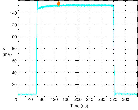
|
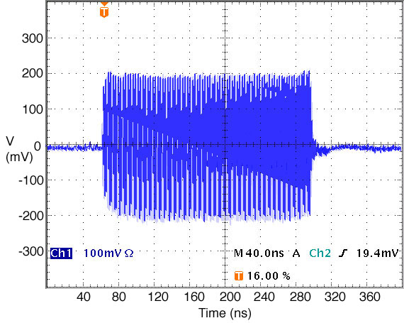
|
||||
| (a) Low-pass filter circuit | (b) Circuit frequency response | ||||
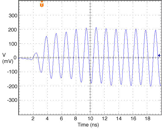 |
|||||
|
|||||
|
|||||
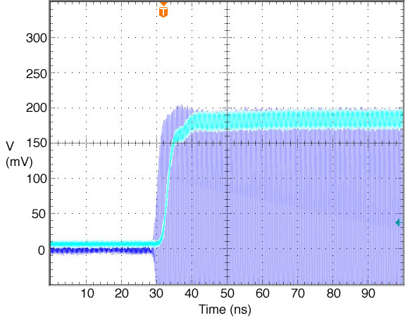 |
|||||
|
|||||
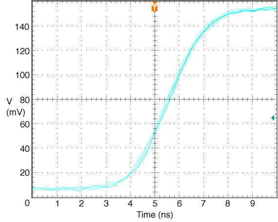
|
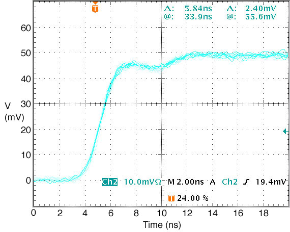
|
||||
|
|
||||
|
|||||
Two Mini-Circuits mixers were used for the test: a low power ZFM-2000 (requiring a +7 dBm LO input with a max. RF input of +1 dBm) and a high power ZP-5MH (+13 dBm LO, +9 dBm max. RF). The higher power mixer was predicted to have a faster rise time. For both mixer tests, a Mini-Circuits SBLP-200 low-pass filter, with a cutoff frequency of 200 MHz, made up the third processor stage. The response of the two mixers is shown in Fig. 3.16. The first obvious feature to note is that both processors replicate the bunch train signal, performing exactly as predicted by the simulation shown in Fig. 3.13. The rise times of the two mixers are also different: the 10-90% time for the high power mixer (Fig. 3.16(c)) is around a nanosecond faster, at 2 ns, than the low power mixer (Fig. 3.16(b)), with each using the same low-pass filter on the IF output. The delay time between input and output was the same for both mixers at ~2 ns.
However, the output of the high power mixer is not as smooth as that of the low power version: there is an extra artifact that appears on the leading edge of the pulse (Fig. 3.16(c)) that is not present on either the original pulse (the blue trace in Fig. 3.16(a)) or the low power mixer output. The signal oscillation that appears on the two traces in Fig. 3.16(a) is not a feature of the processor circuit but a result of crosstalk between the SMT03 pulse generator and the oscilloscope inputs used to record the signals (cf. Fig. 3.16(b)). The timing jitter that appears on the pulses is due to the lack of phase reference between the DG535 square wave generator and the SMT03.
In summary, the lower power mixer (ZFM-2000) is recommended for use in the IPFB BPM processor. It is on the order of 1 ns slower to rise than the ZP-5MH, but has a cleaner frequency response, showing no leading edge ripple (which appears with the ZP-5MH) while still replicating the envelope of the BPM signal. It has the added advantage of being cheaper.
As proof of the corrective capability of the IPFB system, extensive simulations have been carried out independently by Steve Smith [58] and Glen White [68]. The IPFB system was modelled in the Matlab subsidiary package Simulink, allowing accurate simulation of each of the electronic components utilised. The Simulink block diagram for the simulation is shown in Fig. 3.17. Included in the simulation were the various system transport delays (beam flight times and electronic component signal delays), basic modelling of the beam-beam interaction, the stripline BPM response to a bunched beam and the fill time and signal response of the kicker. Fig. 3.13 shows the simulated response of the BPM and the BPM processor in Simulink to a bunched beam at 714 MHz.
| Figure 3.17: Block diagram for Simulink simulation of IPFB system. A number of simulated components, such as the BPM processor, are contained within sub-blocks and are therefore not shown. |
|
||||||||||||||||||||
|
| Figure 3.18: Simulated beam position at the IP using corrective intra-pulse fast feedback for an initial offset of 15 nm (~5σy) and kicker gain 2.4×10⁻⁴. |
The simulation was initially set up with a relative beam offset of 15 nm: this is ~5σy. The initial parameters are summarised in Table 3.124. Three different kicker gains were used to measure the gain dependence of the IPFB system. The simulated effect of the IPFB system with a 15 nm beam offset is shown in Fig. 3.18. After a single round trip the IPFB system has corrected the lower beam (blue) and steered it towards the higher beam (red), bringing the two back into collision. After another latency period the IPFB system makes a further correction: this occurs at ~55 ns. The ripple that occurs in the beam position at this point is a result of the delay loop signal rising as the BPM output falls: this can be seen more clearly in Fig. 3.19.
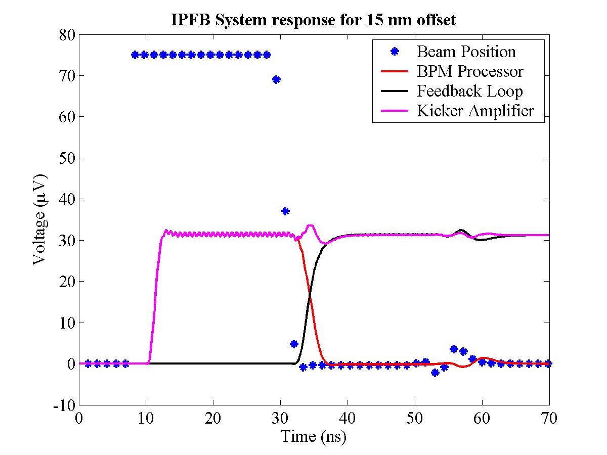
|
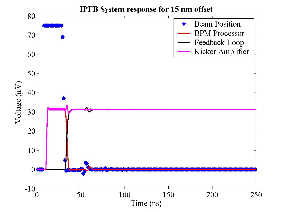
|
||||
| (a) IPFB system response — first 70~ns | (b) IPFB system response — full train | ||||
|
|||||
The signal levels within the IPFB system for the first 70 ns of the train are shown in Fig. 3.19(a); the full train is shown in Fig. 3.19(b). As the beam reaches the IPFB BPM, a corresponding offset is measured in the BPM after 8 ns (blue signal). This beam signal is downmixed to baseband by the BPM processor which shows a corresponding rise at 10 ns (red signal). This signal is fed into the kicker amplifier, which initially tracks the BPM processor signal (magenta signal). After a single latency period of ~22 ns, the incoming beam has been corrected almost perfectly, leaving only a small beam-beam offset and resulting deflection, meaning that only a small signal is now registered at the IPFB BPM after 35 ns. At this point, the signal from the delay loop arrives (black), compensating for the falling BPM signal and keeping the kicker amplifier output at the correct level. The small residual signal from the BPM makes a small correction to the signal from the delay loop, adjusting the beam position with a small correction. The whole process then repeats, with a smaller correction applied from the BPM signal on each successive pass around the delay loop: the small wrinkle in the delay loop signal can be seen at 57 ns, with a corresponding deviation in the kicker signal. Once the incoming beam has been steered to such an extent that the beams are colliding head-on, the BPM processor will no longer produce a position signal, leaving the correct signal now running round the delay loop and being output into the kicker: this can be seen at ~70 ns.
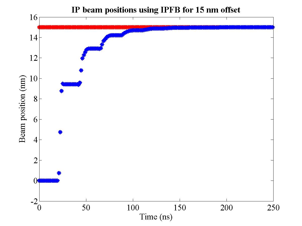
|
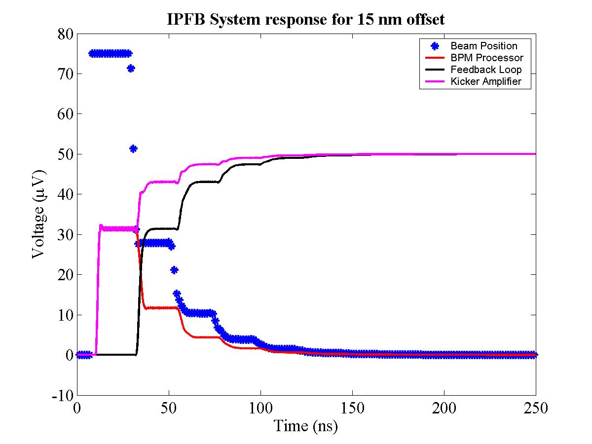
|
||||
| (a) IP beam position | (b) IPFB system response | ||||
|
|||||
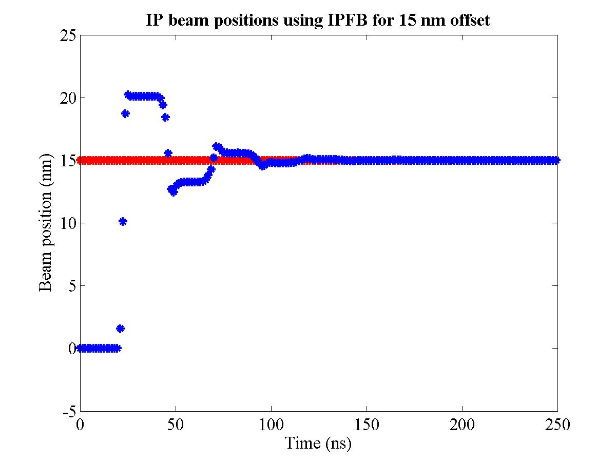
|
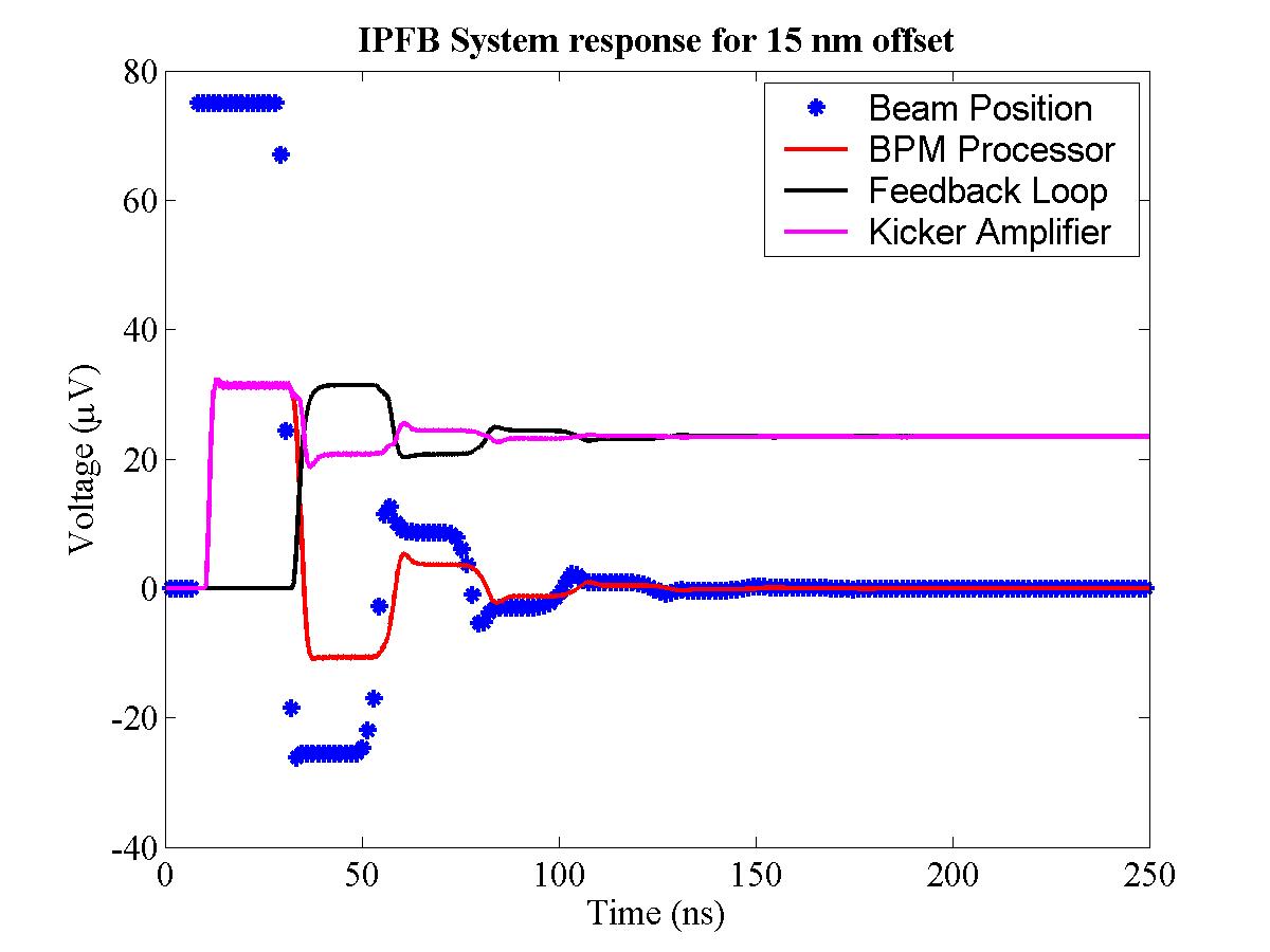
|
||||
| (a) IP beam position | (b) IPFB system response | ||||
|
|||||
Two other simulations, with different kicker gains are shown in Figs. 3.20 and 3.21. Within the simulation there are a number of different gains that control the relative signal levels of each of the different parts of the electronics. One of these gains controls the signal strength that is output by the kicker amplifier to drive the kicker. Setting this gain too low causes the IPFB system to undercorrect the incoming beam, meaning that a further significant correction has to be applied. In this scenario (Fig. 3.20) the system takes longer to close the delay loop, resulting in a less rapid luminosity recovery. Fig. 3.20(b) shows this clearly: instead of coming close to zero with a first pass around the loop at 35 ns, the correction is not large enough, meaning that the system needs several passes before the beam is properly corrected.
On the other hand, setting the kicker gain too high also results in a longer time to recover a head-on collision, but for the opposite reason (Fig. 3.21). The overly strong correction causes the incoming beam to overshoot, missing its intended target. The IPFB system has to make a negative correction and steer the beam in the opposite direction (or, more accurately, less far in the same direction), resulting in the system going into oscillation. Fig. 3.21(b) shows this signal oscillation: at 35 ns the BPM processor signal overshoots beyond zero, since the beam has been overcorrected, and the successive passes around the loop repeat this behaviour. Since the gain is set only slightly too high, this oscillation damps out with successive passes around the delay loop; however, for very high gain settings, the system can oscillate continuously and even make the situation worse, as the beam is steered further and further from a head-on collision with each successive correction.
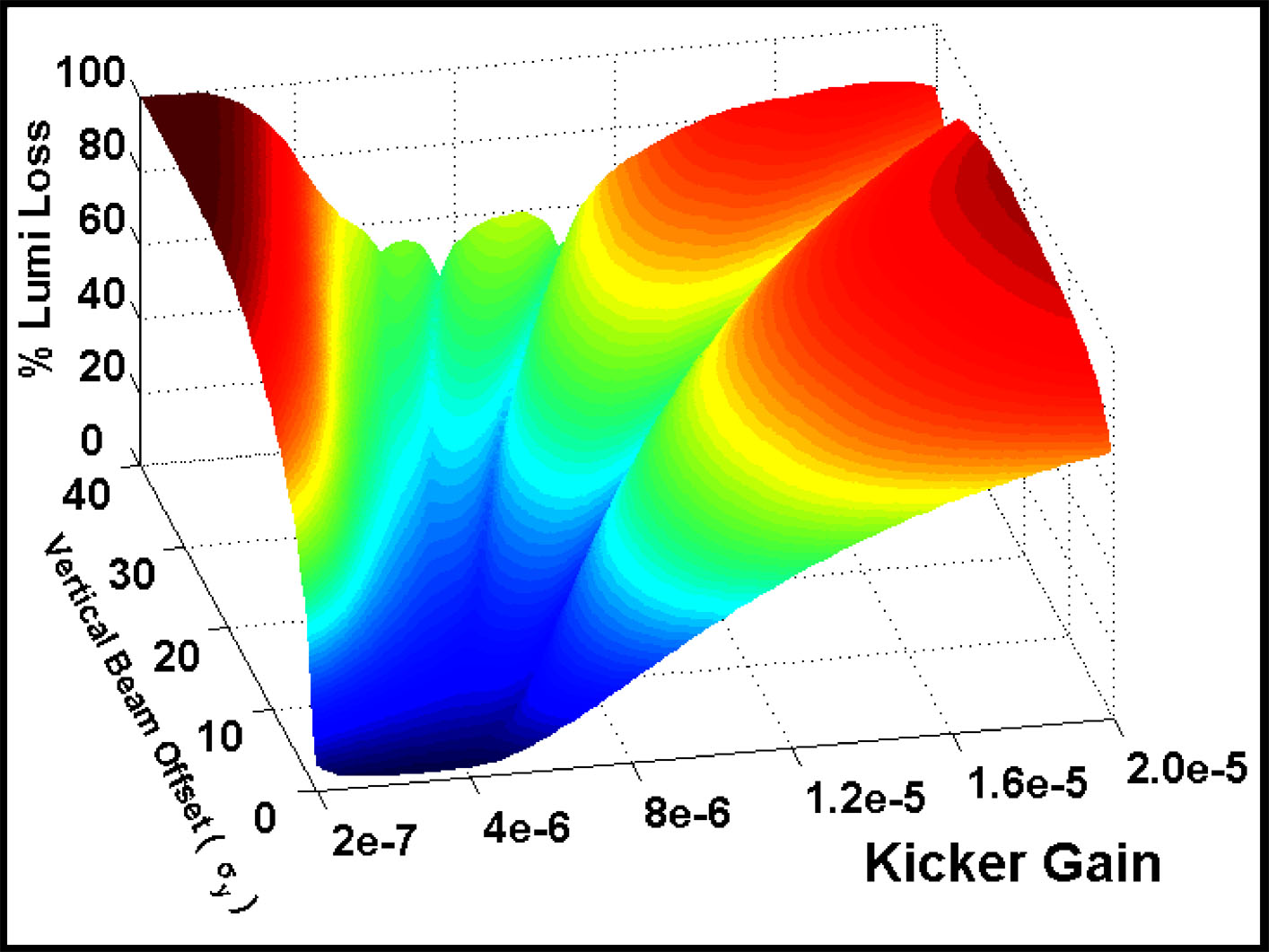
|
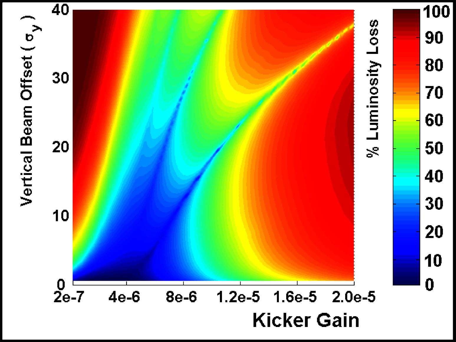
|
||||
|
|||||
The simulations detailed above are incomplete, however, since only a linear model is used for the beam-beam interaction (linear relationship between beam-beam offset and kick strength). Detailed examinations of the effect of the IPFB feedback gain have been carried out by Glen White, using GUINEA-PIG to accurately model the effects of the beam-beam interaction [68]. The effect of the IPFB system on the luminosity of the NLC for different feedback gains is shown in Fig. 3.22. These simulations demonstrate the effectiveness of the IPFB system in correcting a relative beam-beam offset and the ability of the system to correct such an offset well within a single bunch train.
More detailed simulations, also undertaken by Glen White, indicate that for random (Gaussian) noise on the bunch position within a train, the IPFB system does not improve the luminosity [68]. In fact, for random bunch-to-bunch jitter, the feedback system actually makes the situation worse. However, given the sources of such beam jitter, the evidence presented by these simulations indicates that the IPFB system makes a valuable correction to the relative offset between the two bunch trains and recovers a significant amount of luminosity that other feedback systems are unable to correct for (see Section 3.1).
| Figure 3.23: Overhead view of the SLAC Linear Collider, showing the location of the linac, damping rings, electron and positron storage rings and the various experiments [69]. Sector 2 is the section of the linac between the entry and exit points of the damping rings on the left of the picture. |
Having demonstrated the intended IPFB system operation and its effect in luminosity recovery, a full system beamline test was proposed. Such a test was deemed necessary in order to measure the behaviour of the IPFB system in areas that the simulation was unable to accurately model, such as the interaction of the beamline components with the beam itself. Two possible locations for such a test were suggested: Sector 2 of the SLAC SLC accelerator and an unused region of the test accelerator for the Next Linear Collider, the NLCTA (also based at SLAC).
An overhead view of the SLC is shown in Fig. 3.23. The section of the accelerator that was originally considered for use by an IPFB beam test is Sector 2, towards the front end of the linac. The start of Sector 2 encompasses the region of the linac either side of the Damping Rings, referred to as the Damping Ring Injection Point (DRIP). A blow-up of 12 m of the first section of the linac at Sector 2 is shown in Fig. 3.24. The DRIP covers approximately the first 8 m of Sector 2, up to the start of the schematic. The region downstream of the DRIP — the ASSET (Accelerator Structure SETup) region — is currently occupied by the Collimator Wakefield experiment (for details, see [70] and related material, such as [71]).
|
|||||||||||||||||||||||||||||||||
| |||||||||||||||||||||||||||||||||
| Figure 3.24: Blow-up of 12 metres of the first section of Sector 2 of the SLAC linac. The DRIP finishes approximately at the start of the schematic. The wakefield region is between the two collimators at 8.06 m and 11.17 m; the ASSET chicane is downstream of the wakefield box, between the two vacuum valves at 12.09 m and 15.13 m and is marked ‘8’. Measurements are in metres (adapted from [73]). |
The beam parameters for the SLC in the region of Sector 2 are summarised in Table 3.2. The fixed target experiments (based historically within both SLAC End Stations, but now housed only within End Station A) make use of very different beams to that of the colliding beam experiments (such as BaBar and SLD): the current fixed-target experiment is E158. In an experiment designed to measure the electro-weak mixing angle through Møller scattering, E158 will direct a beam of longitudinally polarised electrons onto a hydrogen target housed within End Station A (see [74] for full details). To maximise the event rate, the electron beam is initially intended to be a 100 ns CW beam of 6×10⁸ particles per bunch, rising to a 300 ns long beam for a second series of data runs. An IPFB beam test would make use of the short bunch spacing (0.35 ns) and NLC-like train length (100-300 ns) to simulate the conditions that exist for the real IPFB system. It was also suggested that a subharmonic buncher could be used within the SLC injector with a bunching frequency 1/16th of the standard bunching frequency (2856 MHz), giving a 5.6 ns bunch spacing [72].
The intention was to install a series of fast kickers into the ASSET region of Sector 2 around the wakefield box used for the collimator wakefield experiments. A first magnet would steer the beam off-centre, simulating a beam-beam kick. This position offset would then be registered by one of the existing BPM's within Sector 2, which would be commandeered for the use of this beam test. Upon measuring the beam position, an appropriately-modified25 version of the real IPFB system would process the beam signal and feed it back upstream to a second corrective magnet, such as the parallel plate kicker described in Section 3.2.3. The iterative process of correction would then continue as with the true IPFB system, by setting the normalised signal coming from the BPM to zero.
However, a number of problems became apparent with trying to install an IPFB test setup within Sector 2. Firstly, the schedule for installation within the linac would allow access only once every few months. Given this severe limitation on the number of allowed accesses, it was also unclear where the electronics and data acquisition systems would reside. Any failure, fabrication error or design oversight of the feedback electronics would require a delay of up to 6 months before it could be removed or modified, if it were to sit in the accelerator tunnel. However, placing the electronics outside the tunnel in the klystron gallery26 was unacceptable from a system latency point of view. The best alternative that was presented was to keep as much of the system in the tunnel, while running cables up to a DAQ system in the klystron gallery.
In addition to this, it quickly became apparent that the BPM's and associated electronics installed in Sector 2 were not up to the task required of them by an IPFB beam test. While having a position resolution of a few microns, the minimum time resolution was only on the order of 50 ns [56], not suitable even for the subharmonic buncher spacing of 5.6 ns, and certainly undesirable for a fast feedback system intended to work on nanosecond timescales. Finally, there were the numerous associated problems of running parasitically with and to the schedule of another experiment (E158), with no control over beam conditions or running time. As such, an alternative location was used: the NLCTA.
The Next Linear Collider Test Accelerator (NLCTA) was originally designed to test a complete unit of the NLC RF system i.e. the accelerating structures and RF production, distribution and delivery systems that will be used in the NLC [75]. Although the control and timing systems are intrinsically linked with those of the main accelerator, the NLCTA is otherwise entirely independent of the SLC, with its own injector, accelerating structures and beam dump. An overhead view of the NLCTA is shown in Fig. 3.25. There are six sections of the accelerator that are set aside for accelerating structures: only the first four of these are currently in use for structure tests. This gave the possibility of using the last two unused drift spaces for an IPFB beam test.
Since such a beam test would be designed to test the nanosecond-scale response of the feedback electronics for the IPFB system, the experiment was christened FONT: Feedback On Nanosecond Timescales27.
| Figure 3.25: Ground Plan of the NLCTA. The gun, injector and chicane are located at the front end of the accelerator (left), with the spectrometer, beam dump and the majority of the structures on the rear half (right). See also Figs. 5.1 and 5.2; figure adapted from [76]. |
| Figure 3.26: NLCTA pulse-to-pulse beam jitter measurements, taken with the six consecutive striplines situated downstream of the test structures (see Fig. 3.25): the FONT BPM is installed upstream of BPM1761 (see Fig. 4.8). |
|
|||||||||||||||||||||||||||||||||
| |||||||||||||||||||||||||||||||||
The beam parameters, as summarised in Table 3.3, provided a separate challenge for the purposes of a FONT beam test. Although the beam energy is lower28 by more than an order of magnitude than that in Sector 2, the much larger spot size and beam jitter would mean that a comparatively larger kicker voltage would be required in order to kick the beam a measurable amount. The minimum kick required for a measurable beam offset must steer the beam at least as far as the r.m.s. position jitter on the beam [30], meaning that an NLCTA-based FONT system would still have to kick the beam half the distance of one on Sector 229, giving half the kicker voltage and a quarter of the power. As part of the preliminary measurements for FONT, the beam jitter on the NLCTA was measured using the NLCTA striplines: these measurements are shown in Fig. 3.26.
More importantly, the beam used at the NLCTA does not make use of any subharmonic bunching system, meaning that the electrons are injected continuously, resulting in a CW beam bunched at the structure frequency of 11.424 GHz. Thus the same problem of finding a BPM suitable for use at Sector 2 exist to an even greater extent on the NLCTA. A full description of the BPM that was constructed to measure beam position at the NLCTA is given in Chapter 4. In spite of these problems, it was felt that the obvious advantages of using the NLCTA over the main linac were enough to sway the argument in favour of constructing the FONT experiment on the NLCTA. These advantages were:
This is all, of course, within the operating constraints of the NLCTA. Although running beam was not necessary for the structure tests, since the main activity of the NLCTA was RF processing of the structures, it would not be possible to select arbitrarily the operating conditions of FONT. FONT would still be playing second fiddle to the main purpose of the NLCTA — to develop high gradient RF structures for the NLC — but the interference between the two experiments was intended to be minimal. The design, construction and results of the FONT experiment are given in Chapter 5.
Non-destructive measurements of beam position are essential for the effective running of any modern accelerator. A number of different types of device exist for just such a purpose that come under the generic title Beam Position Monitor, or BPM. Each of these types of BPM makes use of the coupling of the electromagnetic field around a charged particle bunch to some sort of conductor, although the methods used for extracting this signal from the BPM vary and are largely dependent upon the type of BPM used. Three of the most common types of BPM used in modern accelerators are:
| Figure 4.1: Field lines and image charge due to a charged particle beam. |
The stripline BPM is essentially a variation on the button, in which the EM-field lines surrounding a charged bunch terminate on some sort of pickup. In contrast, a cavity BPM uses an appropriately shaped RF cavity that is resonant at the bunching frequency. A resonant EM-field is then set up within the cavity as a result of the passing bunch. In each case, the BPM makes use of the EM-field that surrounds the charged particle bunch and its corresponding image charge: this is shown in Fig. 4.1. The image charge that appears on the beam pipe wall results from the termination of the E-field on the conducting beam pipe. In the relativistic limit (v → c), Lorentz contraction of the EM-field means that there is essentially no longitudinal component to the field, resulting in purely transverse electric and magnetic fields [61].
For a beam centred in the beam pipe, this image charge is evenly distributed over the whole circumference of the pipe and travels along the pipe with the charge, as shown in Fig. 4.1. For an electrode mounted on the beampipe wall, with an angular coverage φ, the induced current in the electrode is therefore:
| (4.1) |
for a beam current Ibeam. It is the termination of the field on the electrodes, in place of the beampipe wall, that gives rise to an induced signal on the electrode. For an off-centre beam, the density of field lines, and hence the image charge distribution, changes accordingly. For beams located close to the centre of the beampipe, small changes in beam position (on the scale of the beampipe width) produce a change in image charge at the electrode that is approximately linear [78]. Each type of BPM makes use of this change in image charge distribution in a different way.
The Button BPM is the simplest of the three types of beam position monitor. It consists of a pair of electrodes, for each axis in which the beam position is to be measured, on opposing sides of the beampipe. Although a simple antenna would suffice, the electrode for a button BPM is usually small and circular, hence the name [61]. The current from the button as a result of the image charge is a function of both the button area A and the charge density of the image charge ρ:
| (4.2) |
where C is the circumference of the beampipe [79]. The image charge and current on a button are shown in Figs. 4.2(a) and (b) respectively; note that the image current is just the derivative if the image charge. The resulting voltage out of the button is therefore the image current on the button driven into the impedance of the transmission line used to extract the signal from the BPM, plus the impedance from the BPM itself; this impedance also includes the natural capacitance of the BPM, giving a filter-like profile for the voltage response [80]. This is shown in Fig. 4.2(c).
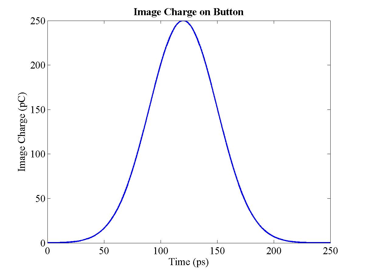
|
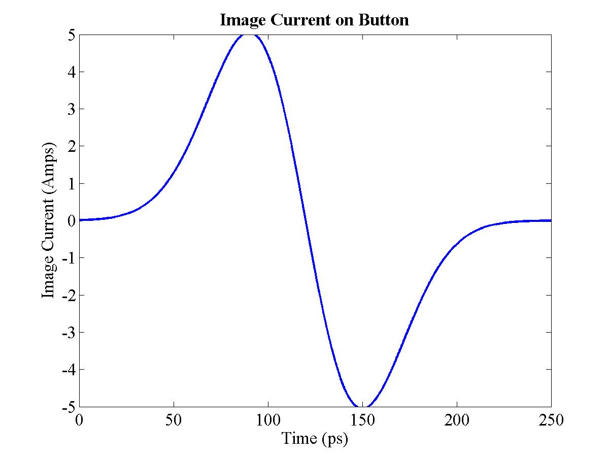
|
||||
| (a) Image charge on button | (b) Image current on button | ||||
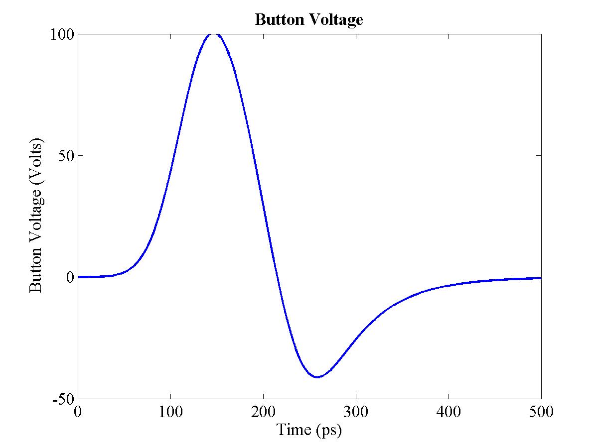 |
|||||
| |||||
|
|||||
Having found the signal from a single pickoff of the BPM, it is necessary to combine the information from each of the pickoffs to extract the beam position. As mentioned in Section 3.3, the signal that is produced by a single pickoff is a convolution of both beam proximity and bunch charge. There are a number of different methods of charge subtraction and position normalisation: the most common are difference-over-sum (Δ/Σ), amplitude-to-phase conversion (AM/PM) and log-ratio processing [61]. Amplitude-to-phase conversion involves converting the two pickoff signals into two signals with identical amplitude, but a relative phase difference that is related to the initial amplitude difference between the two signals [81]. Recombining these two signals of equal amplitude but different phase produces a signal whose amplitude is proportional to the amplitude difference of the raw pickoff signals. Log-ratio processing uses a single hybrid to output a signal that is proportional to the logarithm of the ratio of the two input signals [82].
However, the most popular method of BPM signal processing is difference-over-sum. As given in Eq. (3.4), the difference of the two pickoff signals is divided by the sum of the two signals, giving an output that is a) independent of bunch charge and b) approximately proportional (close to the beampipe centre) to the position variation from the centre of the beampipe:
| (4.3) |
for two pickoffs T and B. The usual procedure is to filter each of the signals at the bunching frequency (or, if cost is an issue, at some lower frequency30) and follow the same processing procedure as outlined in Section 3.3, before calculating Δ/Σ to give the actual beam position.
The stripline BPM is a modification of and improvement over the button BPM. Although it is restricted to bunched beams of a particular bunching frequency, it has a significantly better response at that frequency than the button BPM. A standard stripline BPM replaces the button electrodes of a button BPM with long strips that run parallel to the beam direction; an example is shown in Fig. 4.3. The front (upstream) end of the strip is connected, via an appropriate feedthrough, to a transmission line and thence to the BPM processor. The downstream end is either terminated (usually with a 50 Ω terminator) or left as open circuit. The description below is given for the open circuit version; the treatment for a terminated strip is slightly different, but the resulting signal is the same [56].
|
Figure 4.3: Schematic diagram of a stripline BPM used in the SLC. The BPM consists of four strips — |
For a bunched beam of electrons, the signal from a stripline is as follows. As the bunch passes the front end of the stripline, the image charge passes from the beampipe wall onto the strip. The arrival of the image charge causes a charge separation in the strip: positive charge collects on the inner surface of the strip, forming the image charge, and tracks the actual bunch down the strip as the bunch passes through the BPM. The remaining negative charge that is left from this charge separation is free to move and runs in two directions: half follows the image charge down the strip, while the other half passes out through the transmission line. As such, a negative spike is measured as the electron bunch passes the front of the strip.
Once the bunch passes the end of the strip, the image charge reappears on the wall of the beampipe and continues on as usual. At this point, the positive charge on the inner surface of the strip reflects off the rear end of the strip and travels back towards the front end of the strip, accompanied by the remaining half of the negative charge. Once this charge reaches the front of the strip again, a positive spike of equal magnitude to the initial negative spike is registered. If the length of the stripline is exactly 1/4 of the bunch spacing, the reflected signal arrives exactly half a cycle after the initial beam signal. For a CW bunched beam, this produces the response as shown in Fig. 3.6 [56].
The stripline is therefore resonant at the bunching frequency and produces a very strong signal when filtered at this frequency. For strips of length L, the response of the stripline BPM has the following frequency dependence:
| (4.4) |
As such, the frequency response of the BPM contains peaks at the fundamental bunching frequency and odd harmonics thereof [56]. At even harmonics there are troughs in the frequency spectrum: these are caused by the reflected spikes arriving back at the front of the strip at exactly the same time as a new bunch arrives, cancelling the signal. One therefore designs the dimensions of the stripline around the bunch spacing. This makes it difficult to use a stripline BPM for bunching frequencies much above 1 GHz, particularly from the point of view of impedance matching (necessary to ensure there are no reflections between the strip and transmission line). The methods of BPM signal processing for producing a usable position signal are the same as for the button BPM.
The operation of a cavity BPM is markedly different from the two types of BPM previously described. A cavity BPM takes advantage not of the direct coupling of the EM-field surrounding a bunch to an electrode, but of the ability of a moving bunch to induce an EM-field within a resonant cavity. The cavity is designed to resonate at the bunching frequency of the beam: each bunch that passes through the cavity adds to the resonant field. The behaviour of the EM-field within a resonant cavity is the same as that for a waveguide (see Section 2.3.3). As such, there are a large number of modes at which the EM-field within the cavity can resonate; the magnitudes of each of these modes of oscillation depend on a number of factors, including beam trajectory and the dimensions of the cavity [85]. The two most important modes for the measurement of beam position are the TM010 (monopole) mode and the TM110 (dipole) mode. A cross-section of a cavity BPM, showing the electric fields for the TM010 and TM110 modes is shown in Fig. 4.4.
| Figure 4.4: The TM010 (Monopole) and TM110 (Dipole) modes for a resonant cavity BPM in response to a passing bunch [78]. The dipole mode is only excited for non-zero δx. |
The fundamental mode driven by the bunched beam within the cavity is the monopole mode. However, from the point of view of a beam position measurement, the mode of choice is the dipole mode. The amplitude of the dipole mode depends linearly on the radial beam offset from the cavity centre, and is zero for a beam centred within the cavity [85]. By contrast, the monopole mode is excited most strongly for a centred beam and has no such linear amplitude dependence. Therefore one usually designs the cavity in such a way as to be able to couple out the dipole mode whilst ignoring or damping out the monopole mode: this is done either with the placement of the output coupler (used to extract the beam position signal from the cavity), by coupling out the monopole mode with a coupler that is insensitive to the dipole mode or by using a filter with a narrow bandwidth on the output to select only the frequency of the dipole mode. The position signal can then be measured by using an antenna within the cavity that couples preferentially to the dipole mode (see Fig. 4.4).
The noticeable advantage of a cavity BPM over striplines or buttons is its inherently better position resolution [85]: this is due to the dipole mode signal produced by the cavity. With effective damping and coupling out of the monopole mode, the cavity BPM produces a dominant signal (from the dipole mode) that is only present for an off-centre beam. In contrast, striplines and buttons have to extract this dipole signal from the enormous monopole signal: the electrodes for these BPM types register a signal whether the beam is off-centre or not, meaning that a very small signal (corresponding to an off-centre beam) must be extracted from two very large ones (the raw electrode signals) [86]. This can give an order of magnitude improvement in position resolution for cavities over striplines [87].
It is also possible to improve the position sensitivity of the cavity by increasing the Q through careful design and machining [85]. The Q of a cavity (or a filter) is defined as the ratio of the central frequency to the bandwidth; therefore a 10 GHz cavity with a 10 MHz bandwidth will have Q = 1000. However, the corresponding disadvantage of high-Q cavities is the comparatively poor timing resolution: the large Q causes a corresponding increase in the rise time of the signal. For a bunch train, it is therefore only possible to deconvolve the position of each successive bunch by analysing the signal for the entire train. The output signal from the cavity is effectively the integral over the whole train of the position of each bunch [56]. In addition, a high Q increases the sensitivity of the cavity to external influence, such as physical deformation or external temperature variation. Such external influence can lead to a change in the resonant or coupling frequency of the cavity and hence a change in the measured beam position [85].
As part of the FONT system design, it was necessary to find a BPM best suited to both the NLCTA beam conditions and the FONT requirements. The operating parameters for a FONT BPM are as follows:
All three of the BPM types detailed in Section 4.1 were considered as a possible option for a FONT BPM. The first possibility was to use the existing NLCTA stripline BPM's, or some modification of this design. Within each of the quadrupoles of the NLCTA resides a stripline BPM, of the type shown in Fig. 4.3. The striplines are designed to be resonant at 714 MHz, with a stripline length of 10.5 cm. However, this automatically disqualifies these BPM's from use: a stripline BPM, with electrodes of length L, has peaks in frequency space at odd harmonics of the fundamental frequency (
Also available was the option to use a series of NLC X-band cavity BPM's, developed by Steve Smith and Zenghai Li at SLAC. The intention was to test these cavity BPM's on the NLCTA, giving the possibility of integrating this test with the FONT program by utilising one as the FONT feedback BPM. However the inherent problems with using cavity BPM's ruled them out. Firstly, the rise time associated with a high-Q cavity is such that it would be impossible to resolve beam position on a bunch-by-bunch basis, which is essential for FONT. Secondly, the processing scheme required for a cavity is very different from that for a stripline BPM (and hence the IPFB design), meaning that the use of a cavity BPM would automatically exclude the use of the intended BPM processing scheme.
The best available option was therefore to construct a simple button BPM, designed specifically to be resonant at X-band. It was suggested that it would be possible to tune the pickup antennas of a button BPM to be strongly resonant at X-band and therefore give an enhanced response to the NLCTA beam [30]. It also became clear that constructing a BPM of this kind would be possible from commercially available vacuum components. A design was conceived by Marty Breidenbach and Josef Frisch at SLAC; that design is detailed in the following section.
| Figure 4.5: The X-band BPM designed for use in FONT at the NLCTA. The central spherical cube has 6 ports: four are used for position electrodes, with the other two used for the beampipe flanges. |
The FONT X-band BPM is shown in Fig. 4.5. The BPM consists of a number of standard vacuum components, all of which are commercially available. The main BPM cavity, to which all the other components are attached, is called a spherical cube; details are shown in Fig. 4.6. The spherical cube used for the X-band BPM is approximately 1.38 in. (35 mm) in diameter and was purchased from Kimball Physics31. On each of its six external faces it has a 1-1/3 in. (34 mm) ConFlat flange vacuum mount, used to attach other vacuum components. Mounted on four of the six faces are four SMA feedthroughs, which act as the electrodes for the BPM; these are shown in Fig. 4.7 and were purchased from Kurt J. Lesker Co. These are mounted using the same 1-1/3 in. ConFlat flanges, each with a vacuum-sealing copper gasket. One opposing pair of these electrodes is used to measure the x signal, with the second pair used for y. The final pair of faces on the spherical cube were used to mount the spool pieces that connect the BPM to the main beampipe, again using copper gaskets to seal the join.
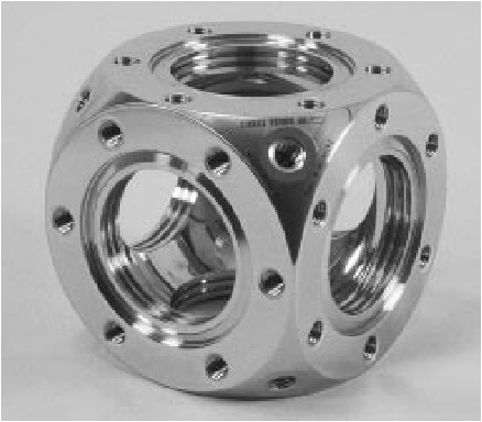
|
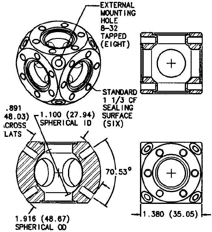
|
||||
| (a) Spherical Cube | (b) Spherical cube dimensions | ||||
|
|||||
|
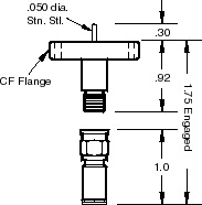
|
||||
| (a) SMA feedthrough | (b) SMA feedthrough dimensions | ||||
| |||||
| Figure 4.8: A blow-up of the NLCTA ground plan (Fig. 3.25) showing the location of the FONT BPM. |
The BPM was installed on the NLCTA downstream of the test structures, upstream of quadrupole QD1760 on girder 17. Fig. 4.8 shows the location of the BPM on the NLCTA. The position of the BPM was advantageous for the FONT experiment as it was located just upstream of one of the NLCTA striplines, mounted inside QD1760, and a toroid (TORO1750) that was located between the X-band BPM and QD1760. This would allow accurate corroborative measurements to be made of both position and charge, since there were no magnetic or obstructive components (such as a collimator) in between. However, since the X-band BPM was downstream of the structures, the spool pieces of the BPM were designed with a particularly narrow aperture to prevent the X-band radiation from the structures from penetrating the BPM.
The selection of the beampipe diameter of the spool pieces for the X-band BPM was important for its effective operation. Since the BPM is located downstream of the structures, any RF that escapes from the structures can travel down the beampipe and into the BPM. Since the bunching frequency of the NLCTA is 11.424 GHz — the same frequency RF that powers the structures — this is the frequency at which the BPM is intended to be most sensitive. Therefore, if any X-band RF were able to enter the BPM, the BPM signal from the beam would be swamped by the escaping RF, rendering the BPM useless.
As such, the beampipe diameter for the BPM was selected to prevent X-band RF from passing into the BPM. In order to do so, one treats the beampipe as a cylindrical waveguide and selects the diameter such that the cutoff frequency is above 11.424 GHz (see Section 2.3.3 for information on waveguides). Of all the modes that are possible within a waveguide, the most common for particle acceleration is the TM01 mode [39]. The cutoff frequency fc for a cylindrical waveguide of radius r is given by:
| (4.5) |
where μ is the permeability of free space, ε is the permittivity of free space and pn,l are roots of the Bessel functions Jn [90].
For the TM01 mode, pn,l = 2.404 (values for pn,l are taken from [90]). For fc = 11.424 GHz, this gives r = 10.0 mm. Therefore, in order to prevent transmission of the TM01 mode, the beampipe inner diameter had to be smaller than 20 mm. However, the beampipe could not be vanishingly small due to the large beam spot size: it was expected that the halo on a beam with σy = 1 mm would probably fill a 1 cm beampipe [30]. The beampipe eventually selected for the BPM was a standard stainless steel tube of 1/2 in. external diameter, also from Kurt J. Lesker Co. With walls 0.035 in. thick, this gives an internal diameter of 0.43 in. = 10.9 mm. With a radius of 5.46 mm, all modes have a cutoff frequency above 11.424 GHz. The simplest mode with the lowest cutoff frequency is the TE11, with pn,l = 1.841 and fc = 16.096 GHz [41].
In order to act as a resonant receiver at 11.424 GHz, it was necessary to tune the electrodes to X-band. The feedthroughs that act as the BPM pickoffs have an SMA connector on the back side, allowing the signal to be coupled out of the BPM (see Fig. 4.7). On the inner side, inside the BPM cavity, an antenna protrudes into the cavity to pick up the signal from the passing beam. It is this antenna that had to be tuned to maximise the beam response. The length of each pickoff was tuned by gradually filing it down until its response peaked at 11.424 GHz32. The response for each pickoff was checked both during the tuning procedure and once the BPM had been installed onto the beampipe.
An Agilent 8719ES Network Analyser [91] was used to measure the response of each pickoff, along with the response of combinations of pickoffs. A network analyser measures the frequency response of a particular device over a specifiable range of frequencies: the full range of the Agilent network analyser used for the BPM measurements was 50 MHz to 13.5 GHz. A frequency sweep with the specified range is output from each of its 2 ports in turn, with the resulting signal either being measured back at the original port from which the signal was output (reflection) or at the opposite port (transmission). Two types of measurement are possible: the S11 response is the signal loss (normally in dB) seen at port 1, as a function of the frequency output from port 1 i.e. the amount of signal reflected back to port 1 from the device being tested; S22 is the same measurement for port 2. The S21 response is a measure of the transmission loss of the device: it is the signal seen at port 2 as a function of the frequency output from port 1. S12 is the opposite: the signal seen at port 1 from port 2.
In making these measurements on the BPM, all the possible combinations of pairs of BPM pickoffs were connected to the two ports of the network analyser and their S11 (S22) and S21 (S12) responses measured. These measurements give some indication of the relative coupling strengths of each pickoff to the beam. Since the transmission and reception properties of an antenna are identical, the S21 measurement for any pair of pickoffs should be identical to the S12 [92]. Two ranges were used for the measurements: a wide frequency band utilising the full range of the network analyser, from 50 MHz to 13.5 GHz, and a narrow frequency range from 9.424 GHz to 13.424 GHz. The narrow frequency range was chosen to be centred around 11.424 GHz with a 4 GHz bandwidth. All four measurements (S11, S22, S21 and S12) were made with each of the six possible pickoff combinations. This gave three S11 measurements for each pickoff and two S21 measurements for each pair of pickoffs. During a measurement, each of the unused pickoffs was terminated with a 50 Ω SMA terminator.
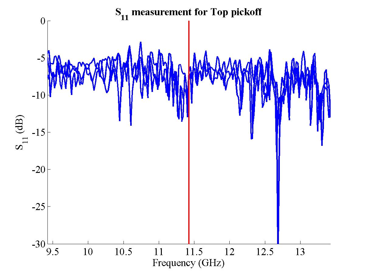
|
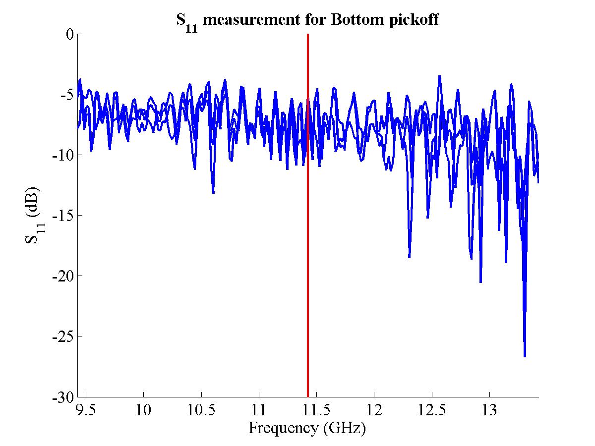
|
||||
| (a) S11 for Top pickoff | (b) S11 for Bottom pickoff | ||||
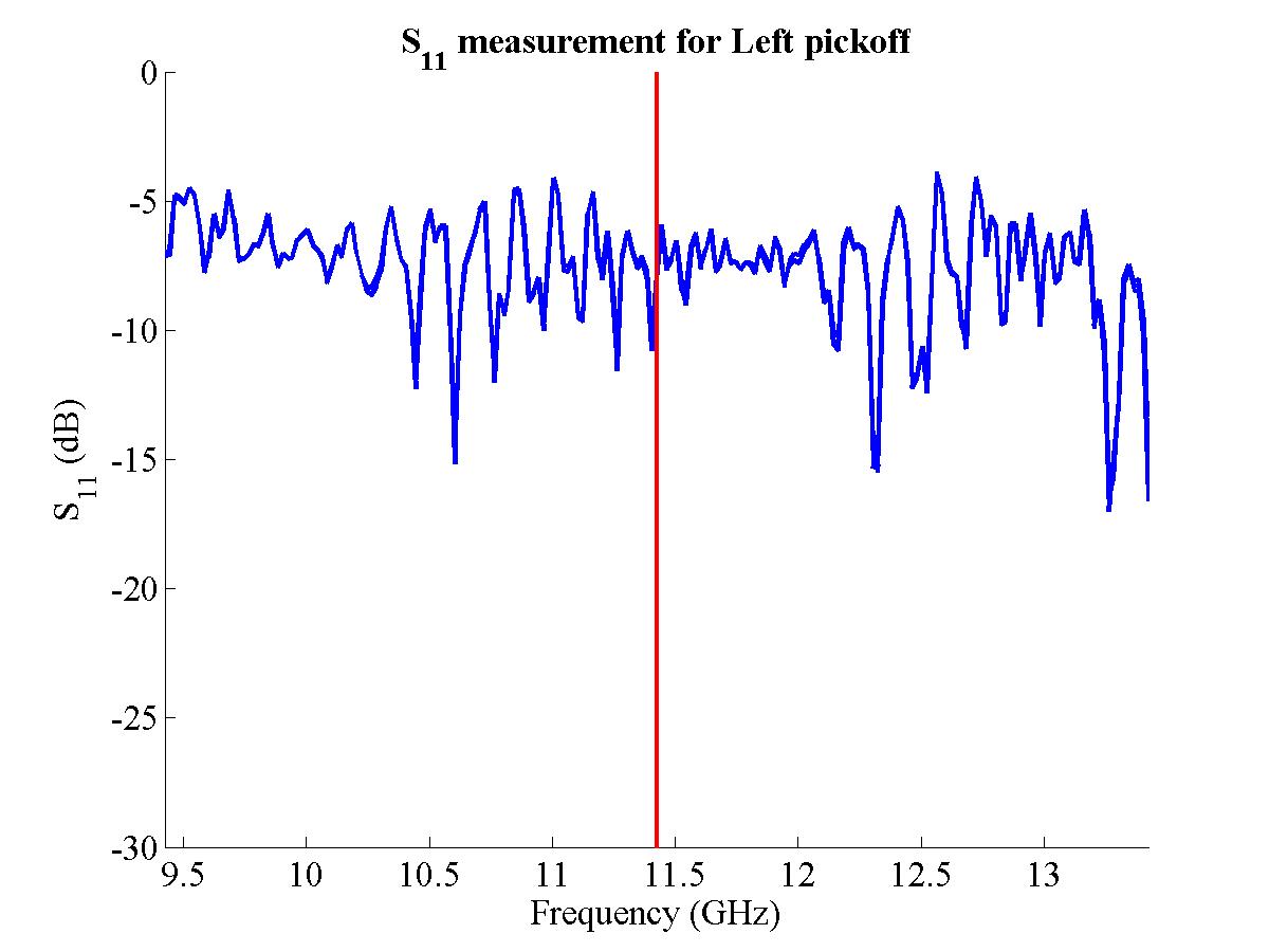
|
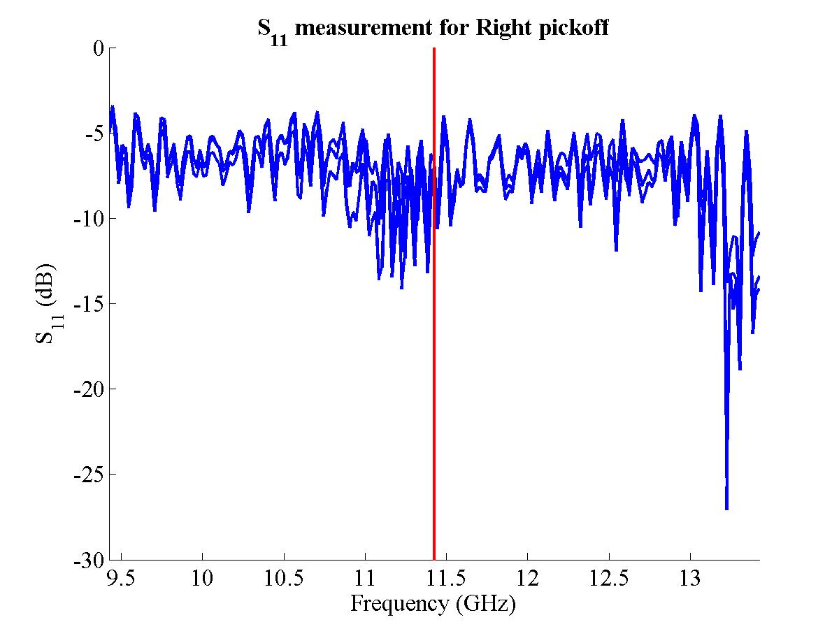
|
||||
| (c) S11 for Left pickoff | (d) S11 for Right pickoff | ||||
| |||||
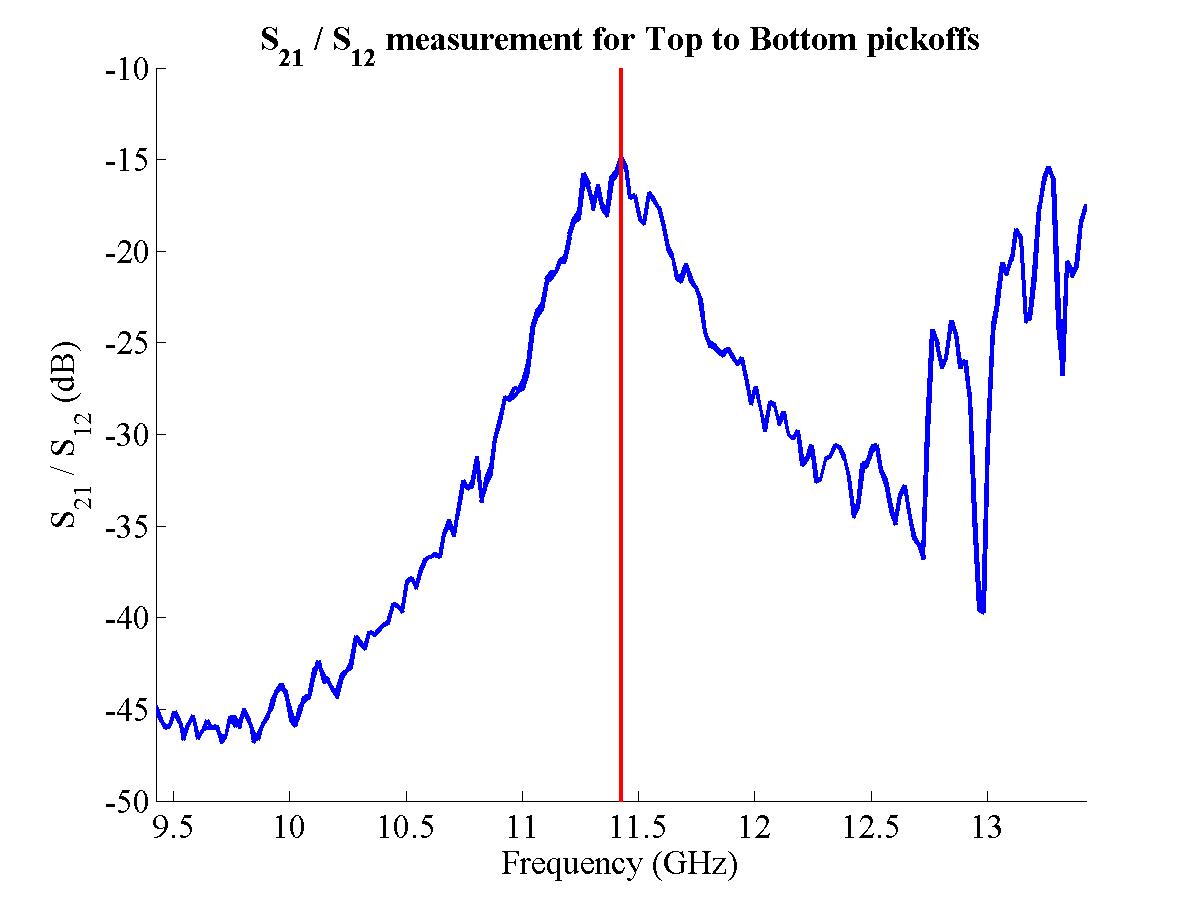
|
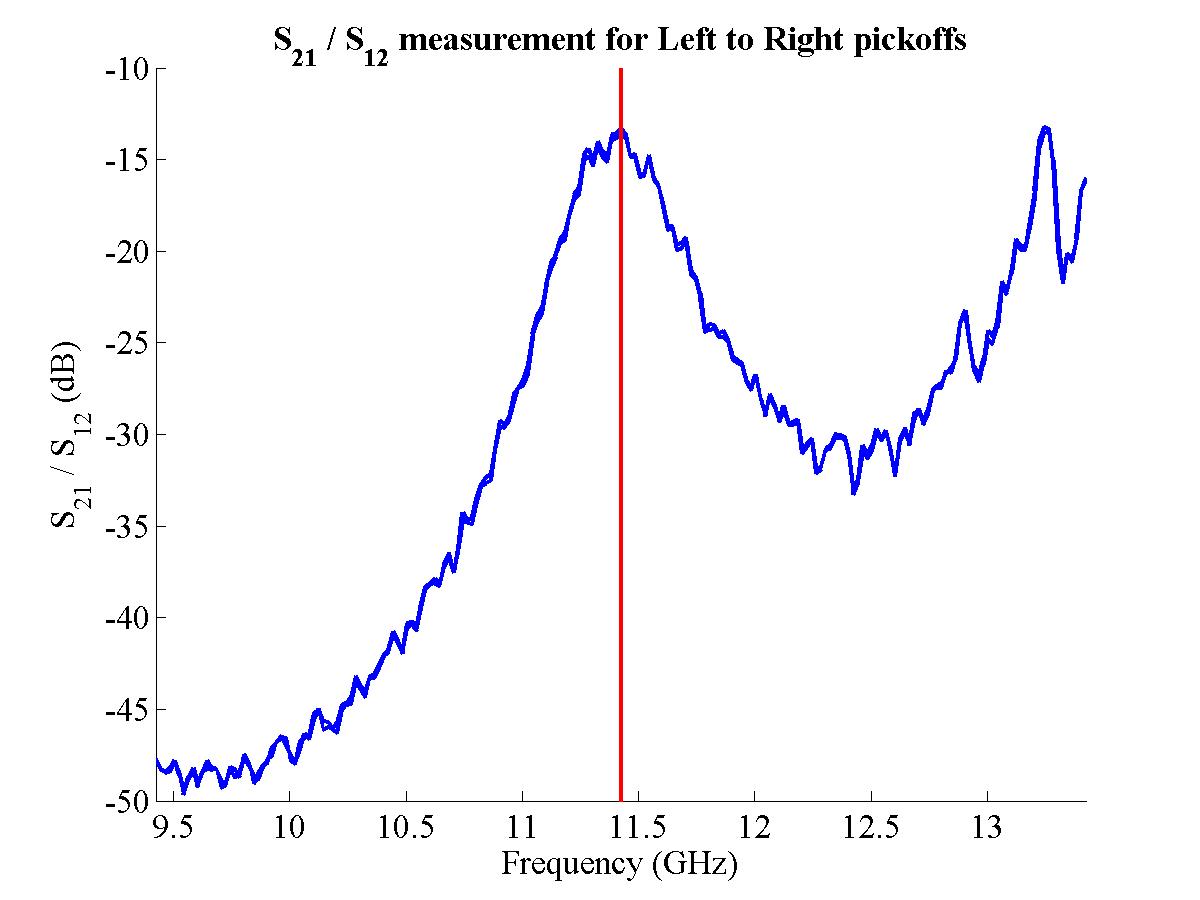
|
||||
| (a) S21 for Top & Bottom | (b) S21 for Left & Right | ||||
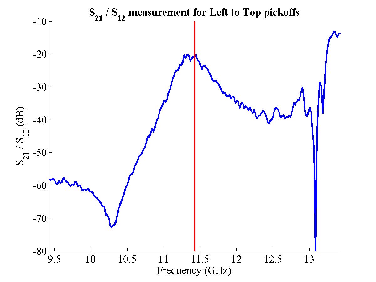
|
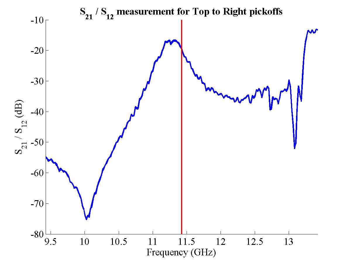
|
||||
| (c) S21 for Top & Left | (d) S21 for Top & Right | ||||
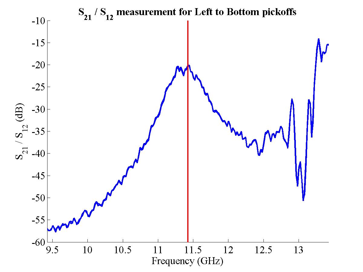
|
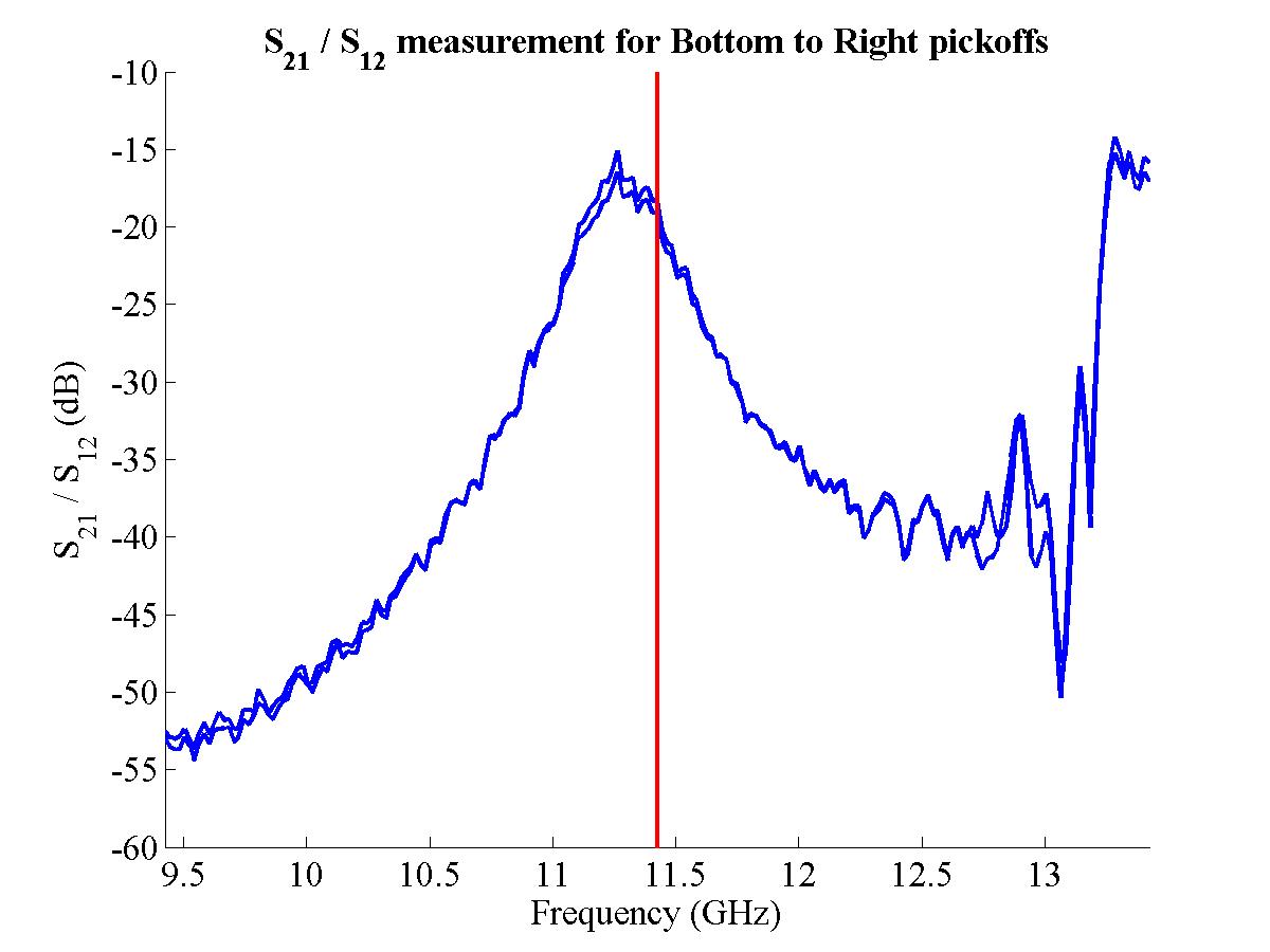
|
||||
| (e) S21 for Bottom & Left | (f) S21 for Bottom & Right | ||||
| |||||
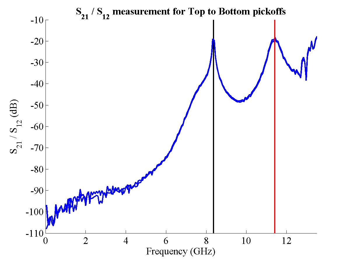
|
|
||||
| (a) S21 for Top & Bottom | (b) S21 for Left & Right | ||||
|
|
||||
| (c) S21 for Top & Left | (d) S21 for Top & Right | ||||
|
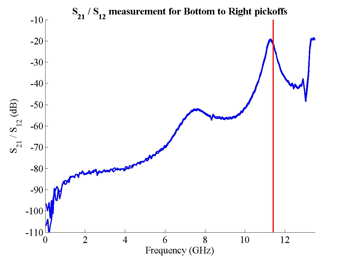
|
||||
| (e) S21 for Bottom & Left | (f) S21 for Bottom & Right | ||||
| |||||
The S11 measurements for each pickoff, using the broad frequency range, are shown in Fig. 4.9. The pickoffs are named according to their position looking downstream at the BPM from the structures. The red line marks the position of 11.424 GHz on the plot. One would expect to see a trough in the reflected signal at this frequency. This is because the electrode behaves as an antenna and emits radiation mostly strongly at its resonant frequency. However, no obvious deviation from the surrounding frequencies is apparent. The likely explanation for such behaviour is that, within an enclosed cavity (such as the BPM), any RF emitted by the pickoff has nowhere to travel. Since the diameter of the beampipe is above cutoff for X-band, none can escape from the cavity: in fact, since the mode with the lowest cutoff frequency (the TE11 mode) has fc = 16.096 GHz, none of the RF within the specified range of the network analyser can escape the cavity. Therefore it is likely that, since it will be reflected within the cavity, it will be reabsorbed by the electrode. As such, any resonant behaviour of the electrode will be nullified as it absorbs the same proportion of RF as it emits for any given frequency. It is therefore likely that the S11 measurement is just a measure of the signal attenuation of the signal path between the pickoff and the network analyser.
The S21 measurements do show a much clearer resonant behaviour. Fig. 4.10 shows the narrow frequency range for the S21 response for each pickoff combination, with Fig. 4.11 showing the wide frequency range. For each pickoff combination, the S21 and S12 measurements are overlaid: the almost perfect match of the two traces on each plot is an excellent confirmation of the identical transmission and reception properties of each electrode. As with the S11 measurements, the position of 11.424 GHz is marked with a red line. In each plot, a peak appears at almost exactly this frequency, indicating that each pickoff is both transmitting and receiving most strongly at X-band.
In Figs 4.11(a) and (b), which show the coupling of opposite pairs of pickoffs, a second peak also appears, at around 8.4 GHz, that is marked with a black line. It is likely that this peak corresponds to the lowest order mode within the cavity, with the frequency corresponding to a wavelength that is approximately the distance between the two electrode feedthroughs (and therefore the outer width of the spherical cube) [92]. It is approximate because the frequency of this mode is dependent on the coupling of the electrode as well as the cavity dimensions. The frequency of the peaks and the corresponding wavelength
| (4.6) |
The actual external width of the spherical cube is 35.05 mm [88]. The difference between this figure and the figures given above (as well as the difference of 0.13 mm between horizontal and vertical dimensions) is most likely due to the coupling of each antenna to the cavity.
| ||||||||||||||
|
With the S21 measurements from Fig. 4.10, it is possible to calculate the relative coupling strengths of the BPM pickoffs to the beam [56]. The S21 transmission loss at X-band, in dB, for each of the six pickoff combinations, is given in Table 4.1. The relative coupling strengths of the BPM pickoffs at X-band can be calculated from these measurements in the following way. If one denotes the signal loss between, say, the top and left pickoffs as ATL and the coupling of the top pickoff to the beam as CT, then one obtains the following set of ratios:
|
(4.7) |
|
(4.8) |
Ideally, the values for CT/CB and CR/CL should be independent of the pair of signal loss figures used in the calculation. In practice, however, a more accurate value is obtained from the S21 measurements by taking an average:
|
(4.9) |
|
(4.10) |
Using the S21 measurements given in Table 4.1 and using the fact that, since these measurements are in dB,
| (4.11) |
| (4.12) |
Converting these from dB to a raw ratio gives:
| (4.13) |
As such, there is approximately a 7% difference in coupling strengths between the top and bottom pickoffs, and a 16% difference between the left and right pickoffs. The vertical pickoffs are more closely matched than the horizontal pickoffs: since the FONT experiment will be concerned with moving and measuring a beam in just the y direction, it was the intention while constructing the BPM to maximise the performance of the vertical pickoffs, hence the better match of the top and bottom electrodes.
Finally, from these measurements it is possible to calculate the Q of the BPM. For a filter, the Q is defined as the width of the resonant peak at the −3 dB point (i.e. the point at which the frequency response has dropped by 3 dB) [62]. For the BPM measurements detailed above, one is not looking at the response of a single pickoff, but pairs of pickoffs: Q is therefore calculated from the width of the peak at the −6 dB point [43]. The following Q values for the horizontal and vertical BPM pickoff pairings are obtained using this method and calculated from the data displayed in Figs. 4.10(a) and (b):
| (4.14) |
As such, the BPM has a low enough Q (particularly in the y direction, in which the FONT experiment is most interested) to respond quickly enough to the beam to perform within the criteria given in Section 4.2, while still responding strongly at the key frequency of 11.424 GHz.
Before undertaking the more complex task of measuring beam position with the new BPM, it was necessary to measure the response of a single BPM pickoff to the beam. This would not only give an absolute scale to the measurements in the previous section (i.e. convert the relative coupling strengths of opposite pickoffs into an absolute coupling strength) but also give a measure of the filtering characteristics, time response and characteristic impedance of the BPM. To do so it was necessary to assemble a BPM processor capable of downmixing a signal at X-band.
The processor design is based upon that outlined in Section 3.3, using an RF mixer to convert the 11.424 GHz signal produced by each of the BPM pickoffs into a baseband signal. However, due to the X-band frequency used for the bunch spacing of the beam, a number of modifications were made to the initial design. The Q (given above) of the BPM would cause it to behave in a similar way to a band-pass filter at the designated resonant frequency of 11.424 GHz. In order to produce a baseband signal, one then mixes the BPM signal with a reference signal, also at 11.424 GHz, producing sum and difference. Normally one would low-pass filter the signal to remove the sum frequency, since it is only the difference frequency that is of interest. In this case however the sum frequency of 22.848 GHz is highly attenuated in most signal cabling (particularly the 3/8 in. heliax used to transmit the signal out of the NLCTA tunnel), meaning that the system as a whole behaves as a low-pass filter. More importantly, the mixers employed also did not have the bandwidth to be able to output a signal of such high frequency.
A block diagram of the components for the first BPM processor is shown in Fig. 4.12. The signal from each pickoff was connected, via a length of SMA cable, to the RF input of a Pulsar Microwave
| Figure 4.12: Block diagram showing the X-band BPM processor used for the single pickoff BPM measurements. A second mixer is used for the other pickoff. |
The intention, as with the IPFB BPM processor, was to downmix the pickoff signal to baseband and transfer this downmixed signal to a DAQ system outside the tunnel. The IF port of each mixer was connected to a 35 m long piece of 3/8 in. heliax cable which was used to carry the signal from the tunnel; a Tektronix digitising oscilloscope recorded each of these pickoff signals. An initial problem occurred in finding an appropriate signal for the mixer LO input. The LO input required for the
A Gunn Diode is a microwave oscillator that takes advantage of the Gunn Effect within a semiconductor (usually GaAs). The Gunn Effect is a result of the band structure that exists within particular semiconductors; examples are shown for the Gallium Arsenide (GaAs) semiconductor most commonly used for Gunn diodes [94]. Fig. 4.13(a) shows the conduction band within GaAs. With a low applied field (i.e. small potential difference) the electrons within the semiconductor reside within the central valley (Γ) of the conduction band. Within this region the semiconductor has a linear I-V relationship. Once the applied field reaches a certain threshold value (Vpeak, as marked in Fig. 4.13(b)), electrons begin to gain enough energy to populate the satellite valley (L). Within this valley the electron mobility μ is considerably lower, with a much larger effective mass: this splitting of the electrons between energy levels causes the semiconductor to behave nonlinearly (see below). Once all the electrons have acquired sufficient energy to populate the satellite valley, the semiconductor takes on the I-V characteristics of this higher energy state and recovers its linear behaviour.
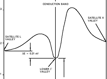
|
|
||||
| (a) GaAs conduction band [94] | (b) GaAs I/V curve [95] | ||||
|
|||||
While the applied voltage is between Vpeak and Vvalley, as shown in Fig. 4.13(b), the semiconductor exhibits distinctly nonlinear behaviour34. This behaviour is due to the superposition of the markedly different I-V characteristics, resulting from the large difference in effective electron mass, of the two valleys within the conduction band. This gives the Negative Differential Resistance (NDR) behaviour shown in Fig. 4.13(b) where, between Vpeak and Vvalley, dI/dV becomes negative. It is this negative differential resistance (usually termed just negative resistance) that is harnessed by the Gunn Diode [95].
| Figure 4.14: Creation of a Gunn domain within n-doped GaAs [94]. Charge perturbation between A and B causes a net positive charge distribution, giving rise to an initial Gunn domain (solid line); this increases with time as it travels towards the anode (dashed line). The horizontal axis indicates the direction of majority carrier flow for a strip of length L. |
In order to create a Gunn diode, a strip of n-doped GaAs is biased with a voltage V such that
By AC coupling the signal at the anode it is possible to create a microwave frequency RF signal: this device is known as a Gunn diode. The signal is usually tuned and enhanced by placing the Gunn diode within a resonant coaxial cavity, the dimensions of which set the output frequency of the diode [95]. Tuning the output frequency is achieved by inserting a rod into the resonant cavity to adjust the resonant frequency; a screw is used to retract the rod from the cavity and change the resonant frequency [96]. It is also possible to drive the cavity at a particular frequency, causing it to resonate with a desired RF signal and behave as an RF amplifier. In addition, running the Gunn diode with a pulsed voltage bias can produce a higher output power. Heat dissipation is important for the diode as a high temperature, resulting from poor heat dissipation, can cause breakdown within the bulk semiconductor. Pulsing the voltage allows higher peak output powers to be reached without damaging the diode.
The Gunn diode used for the X-band BPM mixer LO input was a Microwave Device Technology MO86651-M02 X-band oscillator. The diode is designed to be operated by a pulsed 12 V signal: to provide this signal a separate circuit, designed by Josef Frisch, was assembled. The circuit diagram for this circuit is shown in Fig. 4.15. This circuit requires two inputs: a NIM trigger input and a ~16 V DC power supply input. This DC input was adjusted to set the output pulse to exactly 12 V, since the Gunn diode is very sensitive to variations in this voltage pulse: too low and the output power begins to drop rapidly; too high and the diode starts to draw a large amount of current, causing it to overheat [30]. The switching action of the 3904 transistor allows current to flow through the 3906 transistor in time with the NIM pulse. The 3906 in turn switches on the pair of 2222 transistors which provide the 12 V pulses for the Gunn diode.
| Figure 4.15: The timing circuit used to supply the +12 V pulse to power the Gunn diode. The circuit takes a ~16 V DC input, plus a NIM input that provides the timing and pulse shape. |
| Figure 4.16: The Gunn diode mounted to its timing circuit: the adjustment screw is mounted on the left hand side of the waveguide assembly. |
This timing circuit was mounted onto the back of the Gunn diode waveguide assembly: this is shown in Fig. 4.16. The main chassis of the diode was used as the ground, with the output of the timing circuit connected to the input pin of the diode itself. The two input signals (NIM and +16 V DC) for the timing circuit were carried on two coaxial cables into the NLCTA tunnel. The Gunn diode was initially designed to be used on its own to provide the X-band reference signal for the X-band BPM mixers. However it was not possible to check that the Gunn diode would be phase locked to the beam signal; nor was it possible to set the output frequency to exactly 11.424 GHz. The Gunn diode signal path was therefore modified slightly to allow an external signal to cause it to lock to the beam phase and frequency. This was achieved by driving the Gunn diode with the X-band reference signal from the NLCTA RF system, as mentioned above (see Fig. 4.12). The reference input causes the resonant cavity of the Gunn diode to oscillate at a particular frequency — in this case 11.424 GHz — exciting the diode to resonate at this frequency.
| Figure 4.17: The Gunn diode with its timing circuit attached, and mounted to a waveguide T connector. The two isolators to the left and right of the Gunn diode carry power in from the reference signal to phase lock the diode output (grey), and out from the diode to the BPM mixers (yellow). The two cables appearing from the top are the NIM trigger input (left) and timing circuit 16 V power supply. |
This reference signal input was assembled from a pair of RF isolators, attached to a waveguide T connector: the experimental setup is shown in Fig. 4.17. An isolator is a device that allows RF power to pass through it one only one direction35. One isolator allowed the X-band reference signal to pass into the Gunn diode, while preventing any reflections from the diode from interfering with the reference signal input. A second isolator allowed the output of the Gunn diode to pass onto the mixer LO ports, while preventing any RF from reflecting back into the Gunn diode and disrupting the phase locking. The output of the second isolator was then connected to a 4-way splitter to allow distribution to the two mixers; a third output of the splitter was connected to another heliax cable to allow measurement of the Gunn diode output outside the tunnel, with the fourth output terminated with a 50 Ω terminator.
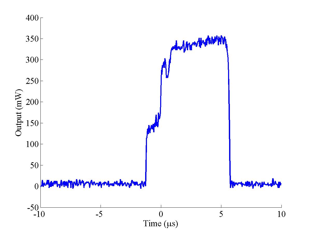
|
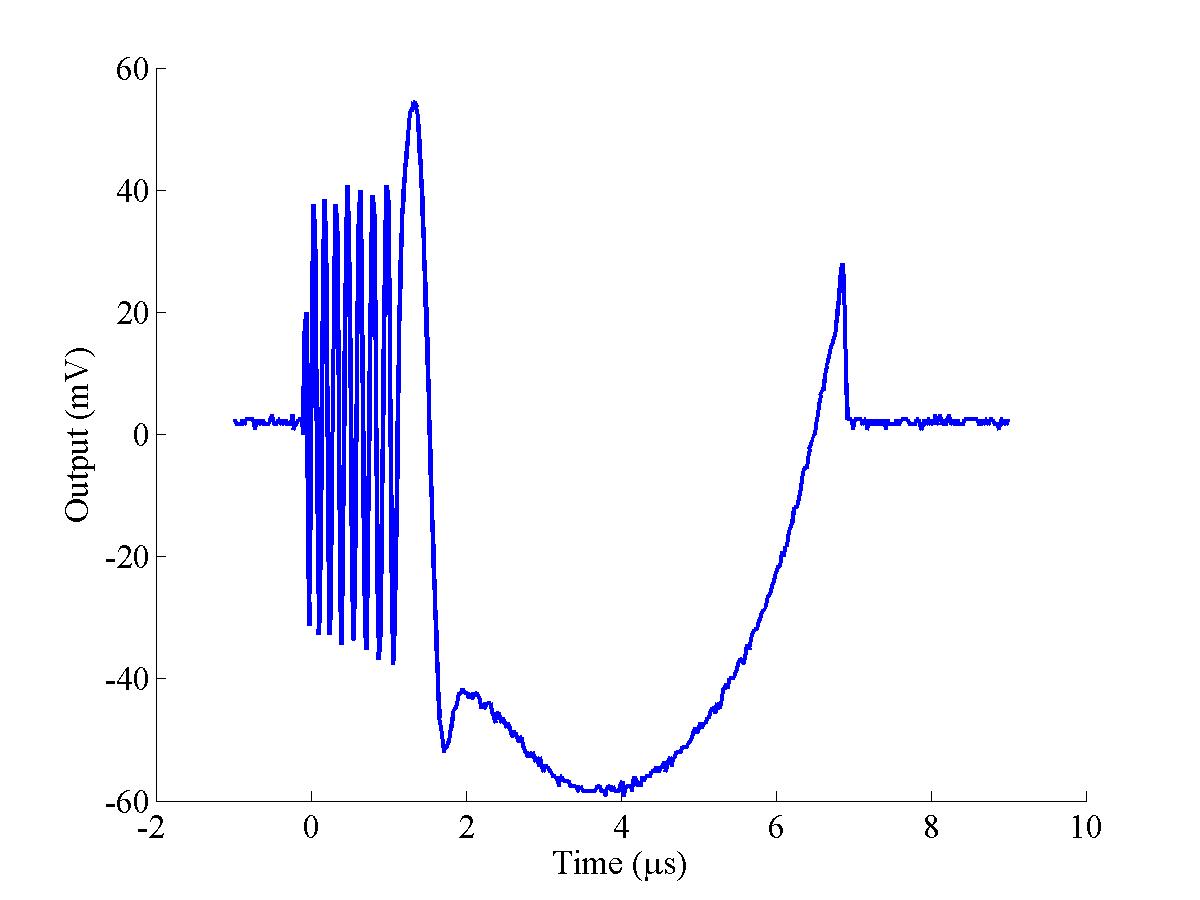
|
||||
| (a) Power Output | (b) Phase lock | ||||
|
|||||
The output power of the Gunn diode is shown in Fig. 4.18(a): at the rear end plateau of the pulse, this is
Having constructed a processor to process the signal from a single pickoff, the response of that pickoff could now be tested. The top pickoff was connected to the mixer RF port (as shown in Fig. 4.12), with the other three unused pickoffs terminated. In order to provide a corroborative signal and a measure of the beam charge, the output of the toroid that resides between the the BPM and QD1760 (TORO 1750 — see Fig. 4.8) was also recorded. A Toroid (also known as a “beam transformer”) is essentially a coil of wire wrapped around a ferromagnetic core that is mounted around a ceramic insert in the beampipe [97]. The ceramic insert allows the EM-field surrounding the beam to penetrate the beampipe. The toroid converts the passing beam current signal into a voltage that can be measured: TORO 1750 produces an output of approximately 1.25 V per Amp of beam current [98].
While normally connected to the NLCTA DAQ system, for the X-band BPM tests the output of TORO 1750 was connected to the scope that was used to record the X-band BPM pickoff signals. This scope in turn was connected, via GPIB, to a PC running Matlab inside the NLCTA Control Room, to allow acquisition and storage of the various BPM and toroid signals. For this first series of single pickoff tests, the NLCTA was run in short pulse mode (see Table 3.3). By changing the NLCTA gun it was possible to alternate between the short and long pulse sources, providing either a ~2 ns or ~170 ns pulse. To measure the impulse response of a single BPM pickoff, the short pulse source was used. This would allow a measure of the coupling strength and time response of the BPM.
| Figure 4.19: Response of a single BPM pickoff to the short pulse beam; the plot shows the average of 5 pulses. |
| Figure 4.20: Toroid output for short pulse beam; the plot shows the average of 5 pulses. |
The output of a single BPM pickoff in response to the short pulse beam is shown in Fig. 4.19, with the corresponding toroid output shown in Fig. 4.20; each of these plots is the average of 5 beam pulses. At first glance it is encouraging to see that the BPM pulse tracks the output of the toroid, but with less of the noise that appears on the falling edge of the pulse. However, some features do appear on the BPM pulse: these are discussed in more detail in Section 4.5.2. The coupling strength of the BPM to the beam is defined as the output in volts of the pickoff per amp of beam current. Since this is essentially V/I, the coupling strength of the BPM can also be expressed as a characteristic impedance, ZBPM:
| (4.15) |
To calculate the characteristic impedance of the BPM it is necessary to compare the voltage output of the BPM pickoff to the actual beam current. The current measurement is provided by TORO 1750: since there are no beamline components between the X-band BPM and the toroid, it is acceptable to assume that the current measured by the toroid is the same as that passing through the BPM. However, in order to account for the features that appear on the falling edge of both signals, the integral of both signals must be used for this comparison: the integrated signal gives an output in Volt-seconds that is independent of the response time of the apparatus in question; all that is important is that the signal has settled to a suitable degree. From these integrated signals, the total bunch charge and BPM coupling strength can be calculated. The integrated toroid output, in Amp-seconds (Coulombs), is given by:
| (4.16) |
for a pulse of length (t2 − t1), toroid voltage Vt at time t, data sampling interval of Δt and toroid beam coupling strength of 1.25 V/A. The corresponding equation for the BPM, in Volt-seconds, is:
| (4.17) |
for BPM voltage Vt at time t. Therefore the result of Eq. (4.17) divided by Eq. (4.16) gives the characteristic impedance of the BPM in Ohms. The integral of the BPM and toroid signal outputs is shown in Figs. 4.21 and 4.22 overlaid with the original signal pulse. From this integrated pulse, a preliminary coupling strength for the single pickoff in question can be calculated. In both cases, the integrated pulse at 45 ns was chosen to have reached a suitable level of stability [30]. The data from two separate runs was used: the integrated voltage output for both toroid and X-band BPM is shown in Table 4.2. The average of the two coupling values gives an initial value of ZBPM = 2.77 Ω.
| ||||||||||||||
| ||||||||||||||
| Figure 4.21: Integrated BPM signal for short pulse beam. The raw BPM pickoff signal is shown in blue, with the integral of that signal shown in black. |
| Figure 4.22: Integrated toroid signal for short pulse beam. The raw toroid signal is shown in blue, with the integral of that signal shown in black. |
However, having calculated an initial coupling strength, one must take into account the attenuation of all the components in the BPM signal path to be able to accurately measure the coupling of the BPM proper to the beam. As such, a number of measurements were made using the components that sit in the signal path between the BPM and the scope for data taking. The signal loss for each component was calculated using the same
| ||||||||||||
|
An output frequency of 11.404 GHz was chosen for the RF signal generator for the RF input to the mixer, as it close enough to 11.424 GHz while still providing a measurable 20 MHz IF frequency. The components between the BPM and the mixer are listed in Table 4.3, in order from BPM SMA output to mixer RF input, along with the measured signal loss for each component. The mixer signal loss as a function of RF input power is shown in Fig. 4.23. The average signal loss for the central power range is 6.15 dB: this gives a total signal loss from X-band BPM to mixer of 21.84 dB.
|
Figure 4.23: Signal loss for the |
The signal from the mixer used in the BPM processor to the scope is carried on a 3/8 in. heliax cable that is 100 m in length. Having been downmixed by the processor, the BPM signal is no longer predominantly at 11.424 GHz, but a DC signal approximating the beam pulse envelope. The short pulse of ~4 ns, as seen in Figs. 4.19 to 4.22, corresponds to a frequency of ~250 MHz; at this frequency, the entire heliax cable assembly — consisting of an SMA to N-type adapter, the heliax cable, an N-type to BNC adapter and ~2 m of BNC cable connected to the scope — was measured to have a total attenuation of 3.90 dB. This gives a total signal attenuation — from BPM to scope — of 25.75 dB. This attenuation reduces the output signal power of the BPM pickoff by a factor of 375.6; this corresponds to a reduction in voltage by a factor of 19.4.36
The true voltage output of the BPM pickoff is therefore 2.77×19.4 = 53.8 V/A, giving the top BPM pickoff a characteristic impedance of ZBPM = 53.8 Ω. Using the coupling ratios calculated in Section 4.3.3, Eq. (4.13), it is possible to calculate the coupling strength of both vertical pickoffs:
| (4.18) |
These values compare favourably to the coupling strength originally predicted for the BPM of 40 Ω [30]. It is also an interesting coincidence that the measured coupling strength is very close to the transmission line impedance of 50 Ω.
The second parameter required to characterise the BPM is its time response; this is also possible to determine from the data shown in Fig. 4.19. The time response of the BPM is defined in terms of the associated decay constant in the same manner as a discharging RC-circuit: it was therefore assumed that the BPM behaved in the same fashion as an RC-filter circuit, with an associated RC decay constant (commonly RC or τ, with units of seconds). Functionally, this RC time constant is the time it takes for the output of a discharging RC circuit to reach 1/e (or 0.37) of its initial value [62]. The differential equation governing the behaviour of such a circuit is:
| (4.19) |
where Vi is the circuit input voltage, Vo is the output voltage, and both are functions of time. To obtain Vo as a function of Vi, the solution to Eq. (4.19) is:
| (4.20) |
where τ is a dummy variable for the purposes of integration [62]. The next stage is to accurately model the pulse shape of the incoming beam. The initial assumption was that the charge distribution along the length of the bunch train was approximately Gaussian. This essentially means that the time structure of the beam — Vi(τ) in Eq. (4.20) — has the following shape:
| (4.21) |
where σ is the standard deviation of the charge distribution along the length of the bunch, A is a scale factor and t0 is the time corresponding to the centre of the pulse (the mean position). The usual 1/(σ√) scale factor is here absorbed into A, since A will be scaled to the size of the beam and so incorporates all such scale factors. All units within the exponential are in nanoseconds; A has the units of Volts. The integrand in Eq. (4.20) therefore becomes:
| (4.22) |
where one has now incorporated all of the scale factors into the single constant A. The lower limit is chosen as −20 to allow the integration to be solved numerically: at this point the function is negligibly close to zero. This numerical integration was carried out by the program Maple, giving the following result:
| (4.23) |
where erf is the error function [99]; erf(x) is twice the integral of the Gaussian distribution with mean 0 and variance of 1/2:
|
Having found the functional form of this RC-filtered Gaussian, the next step is to fit this Gaussian with its 4 independent parameters — RC time constant, t0, σ and A — to the data: this was accomplished in Matlab using the fminsearch function. fminsearch takes an input function and, by varying any number of specified input parameters (constants upon which the function is dependent), finds the minimum of that function. In this case, the function to be minimised is a χ2: this is calculated using the data points for the recorded BPM data (such as that shown in Fig. 4.19) and those generated using Eq. (4.23) with the fitted parameters for discrete time intervals. Minimising the χ2 of these two curves involves varying the four input parameters until χ2 reaches a minimum value. For the purposes of the fit, the χ2 was defined in the following way:
| (4.24) |
for k data points yi and fitted function Vo(t) at discrete time ti. For an RC-filtered Gaussian function the fit for one dataset is shown in Fig. 4.24.
| Figure 4.24: RC-filtered Gaussian pulse fitted to raw BPM pickoff data for short pulse beam. |
Fig. 4.24 uses the same raw data shown in Fig. 4.19. Two of the fitted values (RC and σ) are shown on the plot: since one is no longer dealing with a real RC circuit but with raw time constants, RC is given as τ. It is a measure of the validity of the χ2 fit that the value of τ produced by fminsearch is around a nanosecond, as one would expect from the width of the pulse.
It is also possible to model the bunch train as a square pulse. Although functionally this is more complex due to the discontinuities inherent in a step function, it becomes very simple analytically if one splits the modelled response into 3 parts. If one assumes that the bunch train has a uniform charge distribution and passes through the X-band BPM between time t1 and t2, then prior to t1 the response of the BPM is necessarily zero. Between t1 and t2 the response has the form:
| (4.25) |
Eq. (4.25) describes an exponential decay from zero towards the value A: in the case of the BPM pulse fit A is the peak or plateau value of the step function. After time t2, the response becomes:
| (4.26) |
Eq. (4.26) describes an exponential decay towards zero from a value
| Figure 4.25: RC-filtered square pulse fitted to raw BPM pickoff data for short pulse beam. |
Although the fit for the leading edge of the pulse is better than that for a Gaussian pulse, this is offset by the poor fit for the falling edge, resulting in a larger time constant τ. However one can again see that the fitting process produces results of the correct order of magnitude, since τ, at 1.234 ns, is only ~15% larger for the square pulse than the Gaussian fit. It is therefore a plausible deduction that the BPM behaves with characteristics similar to that of an RC circuit, with a time constant on the order of 1.2 ns.
An improved fitting procedure was written by Gavin Nesom in an attempt to characterise the ringing that appears at around 33 ns [100]. The hypothesis was that this ringing was caused by a signal reflection from one part of the processor circuit, which would then travel back to the BPM pickoff, reflect off the pickoff, invert and follow the original signal with a measurable time delay. The fitting routine using fminsearch was modified to model the reflection by inverting, shrinking and delaying the original signal and adding it to the original. The number of fitted parameters was expanded to six to include the magnitude of the reflection (denoted by B) and the time delay between the original BPM signal and the reflected signal, tr. A necessary boundary condition on the fit was that the previous fit parameters of τ and σ are the same for the reflection as the original signal. Both beam models — of RC-filtered Gaussian and square pulses — were used for this improved reflection model.
| Figure 4.26: RC-filtered Gaussian pulse with signal reflection fitted to raw BPM pickoff data for short pulse beam. The number B/A gives the ratio of the magnitudes of the primary pulse to the reflected pulse. |
| Figure 4.27: RC-filtered Square pulse with signal reflection fitted to raw BPM pickoff data for short pulse beam. The number B/A gives the ratio of the magnitudes of the primary pulse to the reflected pulse. |
The results for each fitting method are shown in Figs. 4.26 and 4.27, with various fitted parameters shown in Table 4.437, including the ratio of the magnitudes of the reflected signal to the original signal, B/A. The first point to note is that the quality of the fit is better, as indicated by the smaller relative χ2 for each fit type (cf. Figs. 4.24 and 4.25). Secondly, the proposed model, with a primary signal plus a reflected signal, does appear to fit the data: in fact, well enough to assume that this is actually the cause of the overshoot that one sees on the raw BPM signal.
| ||||||||||||||||||
|
The SMA cable that connects the BPM pickoff to the BPM processor is ~50 cm long, with a Teflon dielectric that gives it a signal transmission speed of 0.6c [92]. The average time delay between primary and reflected signals is 6.21 ns, which, at a speed of 0.6c, is 1.12 m, approximately twice the length of the SMA cable. The likelihood is that the reflection is caused by the connection of the SMA cable with the BPM processor: this could either be the RF input of the mixer, or the 10 dB attenuator connected between the SMA cable and mixer input. The amplitude of the reflected signal is 0.12 of the primary signal: this corresponds to a signal power loss of 18.4 dB. It is therefore impossible that the reflection comes after the 10 dB attenuator (i.e. at the mixer input), since the reflected signal would be attenuated by at least 20 dB from the two extra passes through the attenuator. The measured S11 reflection at 11.424 GHz of a similar 15 dB attenuator38 was 13.15 dB; the average measured S11 for the top pickoff, as shown in Fig. 4.9(a), is 7.3 dB and the measured signal loss in the SMA cable was 0.66 dB, giving a total signal loss of
Eventually, for reasons of convenience and cost, the first two options were chosen. It was also felt that, in the interests of maximising the difference signal (see Section 4.6), the inherent signal loss of highly attenuating cable would offset the advantages detailed above. In measuring a position signal, a small difference signal has to be produced by subtracting the two very large raw signals from opposing pairs of pickoffs: by attenuating the entire signal, rather than just the sum signal used for charge measurement (as is the case with the current processor), there is a corresponding reduction of the difference signal, the very signal one is trying to maximise. Such a deterioration in the signal-to-noise ratio of the difference signal, and hence the BPM position measurement, was deemed unacceptable. The full processing scheme used to measure the short and long pulse position response of the BPM is detailed in the next section.
Although the BPM processor described in the previous section is suitable for use with a single BPM pickoff, a more sophisticated version is required to fully process the signal from opposing pairs of pickoffs. In order to provide a measure of beam position, the simplest method of signal processing is the difference-over-sum (Δ/Σ) method, as described in Section 4.1.1:
| (4.27) |
As such, the signal produced by (T &minus B) is referred to as the Difference signal and (T + B) as the Sum signal. The usual processing method, in the NLCTA striplines for example, is to extract the raw signals from each pickoff, then process the signal offline with some sort of dedicated microprocessor. However, this method of signal extraction is of no use to an experiment that requires an immediate signal response from the BPM: a signal must be extracted from the BPM on nanosecond timescales in order to provide a position measurement rapidly enough to make a number of corrections to the beam position. As such, a new processor was assembled to enable a rapid signal to be extracted from the BPM. The block diagram for the BPM processor is shown in Fig. 4.28; a photograph of the actual setup around the BPM is shown in Fig. 4.29.
| Figure 4.28: Block diagram showing the components for the FONT BPM processor. The components marked ‘Δφ’ are phase shifters. |
| Figure 4.29: The FONT BPM processor. The 4-way splitter carrying the X-band reference signal can be seen in the bottom left of the picture; the top connector carries the reference signal for the sum signal, with the third used for the difference signal and the second used to pass the signal out to the DAQ system outside the tunnel. Semi-rigid cabling is used between the isolators, connected directly to the BPM pickoffs, and the first set of splitters; conformal cable is used between the splitters in the difference path. |
The processor is a variation of the Δ/Σ method as mentioned above. In order to produce each of these signals, the signal from each of the pickoffs is split by a 2-way stripline splitter/combiner39, with one half of the signal used for the sum signal and the other half used for the difference signal. The sum signal was produced by adding the two raw pickoff signals in phase with one another, through another splitter/combiner, and mixing the resulting signal down to DC. This produces a signal whose magnitude is no longer dependent upon position, but only the charge of the passing bunch. Before allowing this signal into the mixer, a 10 dB attenuator is used to prevent this sum signal from overdriving the mixer input and causing a nonlinear signal response or damage to the mixer40. Two phase shifters41 were used in the sum signal path of both pickoffs to ensure that there was no phase difference between the two signals and that the signal attenuation was the same for both signals; the full phase setting procedure is described in Section 4.6.2.
Since the signal processing had to be carried out at both high frequency (11.424 GHz) and high speed (O(5 ns)), it was deemed more advantageous to subtract the two pickoffs before downmixing to provide the required difference signal. The BPM processor takes advantage of the fact that subtracting two in-phase CW signals is the same as adding two out-of-phase signals. In order to subtract the two signals at X-band, a 180° relative phase shift is introduced into the signal path of the top pickoff via another phase shifter. In other words, before combining the signals from the pair of pickoffs to produce the difference signal, the top pickoff signal is delayed by exactly half a cycle of X-band: this is 44 ps. The two out of phase pickoff signals are now added in the same way as the sum signal, through a splitter/combiner. It is apparent that the two signals now being subtracted are no longer identical for a perfectly centred beam, due to the introduction of the 44 ps delay. However, it was expected that such a small time delay between the two pickoff signals (two orders of magnitude smaller than the time response of the BPM; see Section 4.5.2) would produce a negligible difference in signal magnitude and produce an accurate difference signal. In order that both of the pickoff signals used to produce the difference signal were of the same magnitude, a 1 dB attenuator was used in the signal path of the bottom pickoff, at the same relative location as the phase shifter, to match the signal attenuation of the phase shifter. No attenuator is needed before the input to the difference mixer as the subtraction produces a significantly smaller signal than the addition used in the sum path.
A number of improvements were made with the full two pickoff processor over the single pickoff version (Section 4.4), as discussed above. Isolators42 were introduced into the signal path, connected directly to the SMA output connector of each pickoff. This prevents any reflected signal from any of the components in the signal path from reflecting back into the BPM. The cabling between the isolators and first set of splitters was also shortened and replaced with faster semi-rigid SMA cabling. In addition, the cable lengths between components were made as short as possible — usually the length of a single male-to-male SMA connector required to connect one RF component to the next — with only the difference path making use of two short lengths of conformal cable (see Fig. 4.29). Finally, the Gunn diode was replaced with a dedicated X-band amplifier.
| Figure 4.30: Schematic diagram of the X-band amplifier, showing the external dimensions; dimensions are in inches [104]. |
| ||||||||||||||
|
| ||||||||||||
|
In order to provide a stable X-band reference signal for the BPM, the Gunn diode arrangement (as described in Section 4.4.3) was replaced with a dedicated X-band amplifier. The amplifier used for FONT was produced by Transcom Inc. of Taiwan; the specifications for the amplifier are shown in Table 4.5, with the external dimensions shown in Fig. 4.30. The amplifier requires a 12 V, 1.5 A DC voltage supply: this was provided by a DC power supply unit located outside the tunnel and carried into the tunnel via BNC cable. The same X-band reference signal used as the source signal for the Gunn diode was used for the amplifier, carried into the tunnel from the NLCTA RF system via 3/8-in. heliax cable. Before installation, the gain of the amplifier was briefly measured with a known input power, at 11.424 GHz, supplied by a Gigatronics Model 7100 Synthesised Signal Generator: the results are shown in Table 4.6. It is clear from this brief test that the output power tops out at just over 31 dBm, corresponding to a maximum output power of 1.35 W; it should be noted that this exceeds the maximum power output of the Gunn diode (cf. Section 4.4.3). For a supply voltage of 12.003 V, the amplifier drew a measured current of 1.31 A. Also measured were the phase and frequency stability of the amplifier output signal: no measurable deviation from the specified operating parameters was observed.
| Figure 4.31: The X-band amplifier: the RF input is on the left, with the X-band reference signal brought in on 3/8-in. heliax. The output is on the right: a 2 dB attenuator is used to drop the signal to the correct level. Power is supplied via the two pins at the top of the amplifier. The fan on the left is used to cool the enclosure; the amplifier is mounted to a black heat sink to prevent it overheating. |
The amplifier was installed underneath the beampipe in the NLCTA tunnel in place of the Gunn diode. Before installation it was mounted to a large metal heat sink, since the large quantity of heat generated by the amplifier during operation caused it to overheat and the power output and gain to drop significantly. The underside of the amplifier was first covered with a silicon gel, to provide a good thermal contact, then firmly bolted to the heat sink with four bolts. Once installed in the tunnel, the amplifier assembly was protected with lead shielding to prevent radiation damage. A 12 cm fan was placed within the shielding to encourage air flow and provide further cooling for the amplifier; small gaps were left at various points in the shielding to aid air circulation. The full amplifier assembly is shown installed in the NLCTA tunnel with some of its lead shielding in Fig. 4.31. As before, the output signal from the amplifier was split using a 4-way splitter/combiner43; this was connected to the amplifier via a 30 cm length of conformal SMA cable and an attenuator. The attenuator was used to set the reference signal for the mixers to the correct power and was set at 2 dB. Using one of the unused outputs of the 4-way splitter, the power output of the amplifier (and therefore the LO input power to the BPM processor mixers) was measured to be 17.44 dBm, compared to a required input power of 17 dBm. After 24 hours continuous running the power output had dropped to 16.87 dBm; this level remained unchanged after a further 24 hours. The fourth output of the 4-way splitter was connected to a power meter outside the tunnel via 3/8 in. heliax cable, and was used to monitor the output power of the amplifier at various intervals during data taking.
In order to provide the correctly phased signals for addition and subtraction within the BPM processor, correct setting of each of the phase shifters (see Fig. 4.28) was essential. The processor contains 4 phase shifters in total: two are used to match the phase of the sum signal44, a third sets one path of the difference signal out of phase by 180° with respect to the other, and the fourth matches the relative phase of the LO input for the two mixers. A fifth phase shifter was used to correctly set the phase of the X-band reference signal once beam running had started. A procedure for correctly setting the phase of each section of the processor was put forward by Josef Frisch and followed on each occasion that a) a component in the processor was changed or b) after a period of inactivity, usually greater than a week.
Since it would not be possible to run the beam while making the processor phase adjustments, another source of X-band signal had to be used. The best solution found was to drive each of the horizontal pickoffs with an X-band source and use the coupling between pickoffs (as shown in Fig. 4.9) to drive the vertical pickoffs. For this X-band source, the fourth output of the 4-way splitter from the X-band amplifier was used to drive the right pickoff via another phase shifter. The two phase shifters in the sum path were adjusted to both be approximately in the centre of their range; the signal path for the top pickoff was then disconnected after the isolator and the free ends terminated with 50 Ω terminators. The unused left pickoff was monitored with an Agilent E4417A Power Meter to measure the power output of the X-band source. The X-band source phase shifter was then adjusted until the output of the sum mixer reached a maximum: this indicated that the signal passing into the BPM and through the connected portion of the processor, via the bottom BPM pickoff, was in phase with the X-band reference signal when it reached the mixer45. The output of the sum mixer was measured at 18 mV, with a power output at the left pickoff of 0.80 dBm.
The bottom pickoff was then disconnected after the isolator, with the free ends terminated, and the top pickoff reconnected. The phase shifter in the top pickoff path of the sum signal was then adjusted until the sum mixer output reached a maximum of 18.5 mV. Finally, the bottom pickoff was reconnected and the output of the sum mixer measured at 37 mV; the two sum phase shifters in the sum path were then adjusted slightly to confirm that the signal output of the sum mixer was at a maximum, before being returned to their optimum positions. The whole procedure was then repeated, this time driving the left rather than the right pickoff with the X-band source signal and monitoring the power output of the right pickoff. There was no measurable difference between these results and those obtained by driving the right pickoff, indicating that the phase setting for the sum signal was likely to be sound; the power output of the right pickoff was measured to be 0.87 dBm. It should also be noted that a −2 mV offset was measured on the output of the mixer: this is present whenever a signal is input into the mixer LO port, of suitable amplitude (i.e. 17 dBm for the
Having correctly phased the two signal inputs for the sum signal, it was then necessary to adjust the difference signal. The X-band source remained driving the left pickoff, with the X-band source phase shifter left unchanged after the sum measurements in order that a consistent phase reference was present. With the top pickoff disconnected at the isolator (and the free ends terminated) and the bottom pickoff connected, the phase shifter on the LO input to the difference mixer was adjusted to make the signal produced by the difference mixer maximally negative46. With a power output of 0.93 dBm measured at the right pickoff, the difference mixer output reached a maximally negative value of −40 mV; adjusting for the −2 mV offset of the mixer gives a value of −38 mV. The bottom pickoff was then disconnected at the isolator (with the free ends terminated) and the top pickoff reconnected. The phase shifter in the difference signal path from the top pickoff was then adjusted to maximise the output of the difference mixer at 35 mV, or 37 mV when accounting for the mixer offset. Finally, the bottom pickoff was reconnected and the output of the difference mixer measured to ensure a zero output: after setting the phase shifter from the top pickoff to its optimum position, the output of the difference mixer was measured to be
A problem exists with this phase setting procedure, however, since it is impossible to use the true source of X-band signal for these measurements: this signal source is the beam itself. Since one cannot run the beam whilst a person is in the tunnel, and one cannot adjust the BPM processor phase shifters from outside the tunnel, the only satisfactory solution was to drive one of the two unused pickoffs with an X-band signal source. It is highly unlikely that the phase of a signal produced by injecting a signal into the BPM through one of the unused pickoffs is the same as that produced by the beam itself. However, the procedure is not completely without value, since one is concerned with the relative difference between the two pickoffs. Given that there was no measurable difference in the setting of each phase shifter when the right, rather than the left pickoff was used as the X-band source, it is probable that the relative phase of each portion of the BPM processor has been set correctly. It is an open question how one could test these settings more rigorously, since one cannot inject an X-band signal into the BPM via the beampipe as the diameter of the pipe is designed not to pass X-band (see Section 4.3.1).
The final part of the phase setting procedure is to correctly set the phase of the X-band reference signal. This was to ensure that the two LO inputs to the sum and difference mixers were exactly in phase with the BPM signal produced in response to the passing beam. An X-band phase shifter was inserted into the signal path of the reference signal before it entered the tunnel to allow the phase to be set remotely. The setting of this phase required the beam to be running, but was not dependent upon the beam pulse type (see Table 3.3). Once running, the beam was steered upwards to produce a positive difference signal. Initially the phase shifter was adjusted to maximise first the sum, then the difference signal. The phase was then adjusted to find the null points (±90° from being exactly in phase, giving zero output; see footnote 45) for both the sum and difference signals.
A phase difference of approximately 20° was measured between the sum and difference output: the phase shifter was therefore set between these two values, 10° away from being exactly in phase with each signal. This 20° phase difference is an indication of the inaccuracy present in the BPM processor phase setting procedure; however, a phase difference between beam and reference of 10° was considered acceptable. For the long pulse beam, a phase slew of approximately 20° was observed along the length of the 170 ns pulse; this was later corroborated by independent measurements made by Chris Adolphsen. The BPM processor is largely insensitive to such a phase slew, as long as the reference signal is close to being exactly in phase with the beam. It was also of note that the majority of this phase slew is present at the leading and trailing edges of the pulse, with the central 100 ns of the pulse stable to ~5°. This final phase setting procedure was carried out more often than that required for the BPM processor, since the reference phase was observed to drift by up to 90° over a 24 hour period.
Although the BPM was designed to measure the full 170 ns long pulse, it was also possible to use it to measure the 2 ns short pulse beam. The advantage of using the short pulse beam is that more trustworthy corroborative evidence is available for the BPM position measurements: as noted in Section 4.2, the NLCTA stripline BPM's were only sensitive to beam pulses around a nanosecond in length. For times longer than ~1 ns, the reflections caused by the striplines (see Fig. 3.6) cancel the original impulse beam response, giving no output. However, for the first 1 ns of the beam pulse, the reflected pulse has not yet had time to arrive at the front edge of the stripline, so a position measurement can be made. It is therefore possible to measure the position of the leading edge of the long pulse beam, but a much more accurate measurement is possible for the short pulse beam.
| Figure 4.32: Blow-up of the area of the NLCTA around the FONT BPM, showing the NLCTA stripline BPM's recorded during the FONT BPM tests (adapted from [76]). The ‘1’ at the end of each BPM ID indicates that y position is being measured (a ‘0’ would indicate x position). |
Data from the NLCTA stripline BPM's is recorded using the NLCTA section of the SLAC Control Program (SCP). The SCP can record both the x and y position as measured by the BPM, plus the Total Measured Intensity (TMIT): the TMIT measurement is similar to the sum signal produced by the FONT BPM processor and is a measure of the beam charge observed by the BPM. Due to the multiplexing used in the stripline BPM data acquisition system, only one plane is recorded for each beam pulse i.e. only x or y can be recorded for any single pulse, plus the associated TMIT. As such, when using the SCP to record data, it is only possible to record beam position for one of the two axes. Two methods of data collection are available: buffered data and correlated data. Buffered data acquisition is the measurement of n consecutive pulses for identical beam conditions. Correlated data, also known as ‘correlation plotting’ is the acquisition of n consecutive pulses while incrementally changing the beam orbit; this usually involves the steering of the beam with one or two dipoles, and correlating the beam position measured at each BPM to the current/field of each dipole.
For the FONT BPM tests, only the y position of the beam was measured, since the FONT BPM was only set up to record the vertical beam position. The SCP was programmed to record the Y position and TMIT of 7 NLCTA stripline BPM's: 1451, 1551, 1651, 1761, 1811, 1871 and 1921. Each BPM is mounted inside a quadrupole magnet: the location of each of these BPM's, along with the FONT BPM, is shown in Fig. 4.32. The most important of these BPM's is 1761, since the FONT BPM is installed just upstream and there are no magnetic elements between them; it is possible therefore to use the position measurement of BPM 1761 as a comparable measurement for the beam at the FONT BPM, since there is only ~40 cm of drift space between the two. The output signals from the FONT BPM processor were brought out of the NLCTA tunnel on 3/8 in. heliax cable and connected to a Tektronix digitising oscilloscope. Using the scope's GPIB interface and a GPIB-TCP/IP interface box, the data for each pulse was extracted from the scope by a PC running Matlab, allowing the DAQ and data manipulation to be integrated into a single Matlab routine.
| Figure 4.33: The raw difference signal produced by the FONT BPM processor for the short pulse beam. Note the large overshoot that appears at 50 ns; plot shows 20 beam pulses. |
| Figure 4.34: The raw sum signal produced by the FONT BPM processor for the short pulse beam; plot shows 20 beam pulses. |
| Figure 4.35: The output of toroid 1750 for the short pulse beam; plot shows 20 beam pulses. The output (until the ringing starts at ~35 ns) is similar to that of the FONT BPM sum signal (Fig. 4.34). |
The sum and difference outputs of the FONT BPM processor in response to the short pulse beam are shown in Figs. 4.33 and 4.34; the corresponding output of Toroid 1750, situated between the FONT BPM and BPM 1761, is shown in Fig. 4.35. For these measurements, the beam was steered as close to the centre of the BPM as possible using the y corrector (YCOR 1650) of QD1650, the quadrupole upstream of the BPM. YCOR 1650 was chosen as there is only drift space between QD1650 and the FONT BPM. The first clear feature is the enormous double peak that appears on the BPM difference signal. Since the difference signal is a convolution of both beam position and charge, this would appear to indicate that the position varied wildly midway through the pulse, since the charge cannot be negative. A greater analysis of this signal overshoot is given in Section 4.7.2.
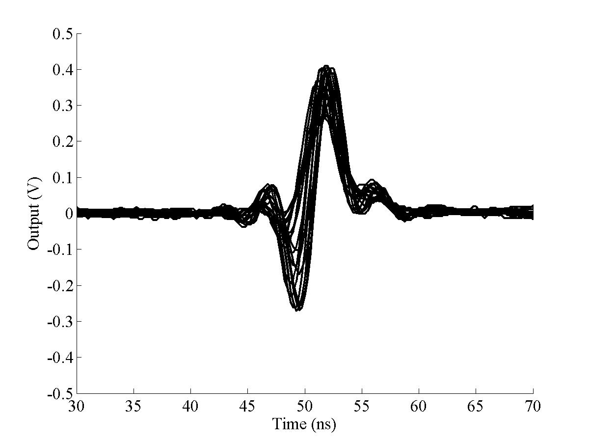
|
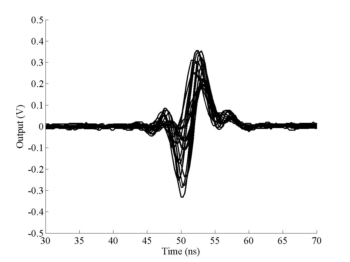
|
||||
| (a) 4.0 G-m | (b) 2.5 G-m | ||||
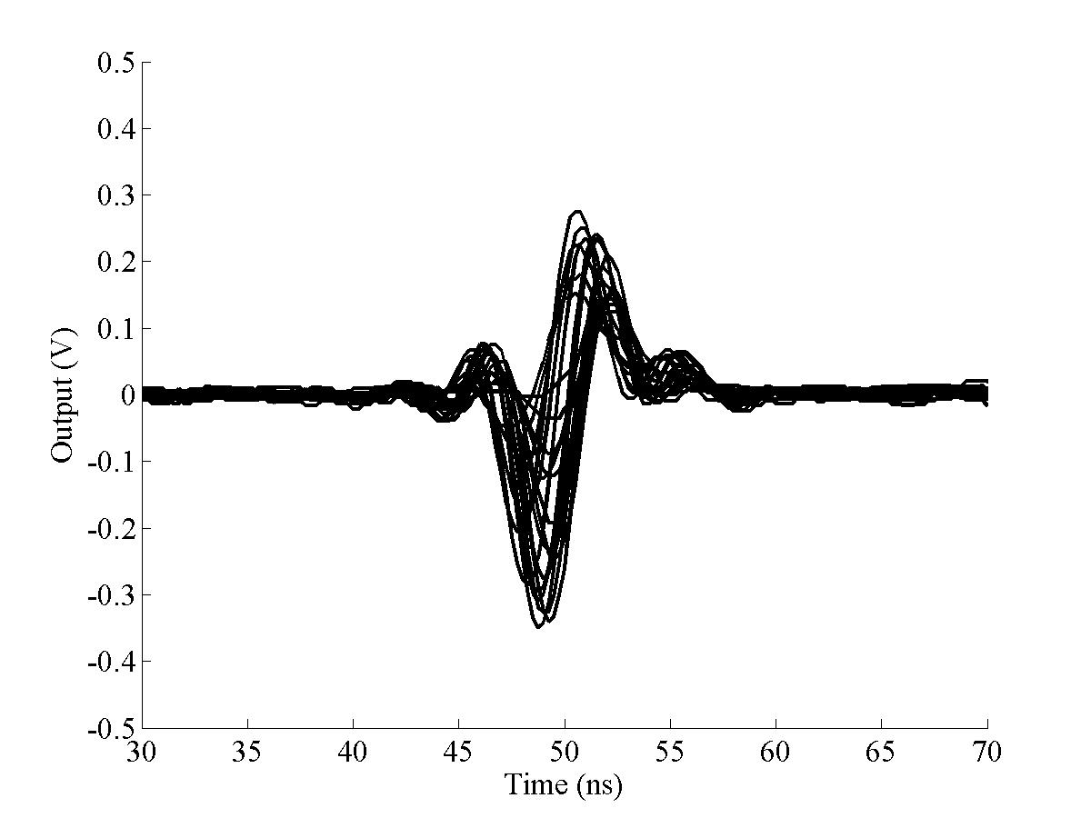
|
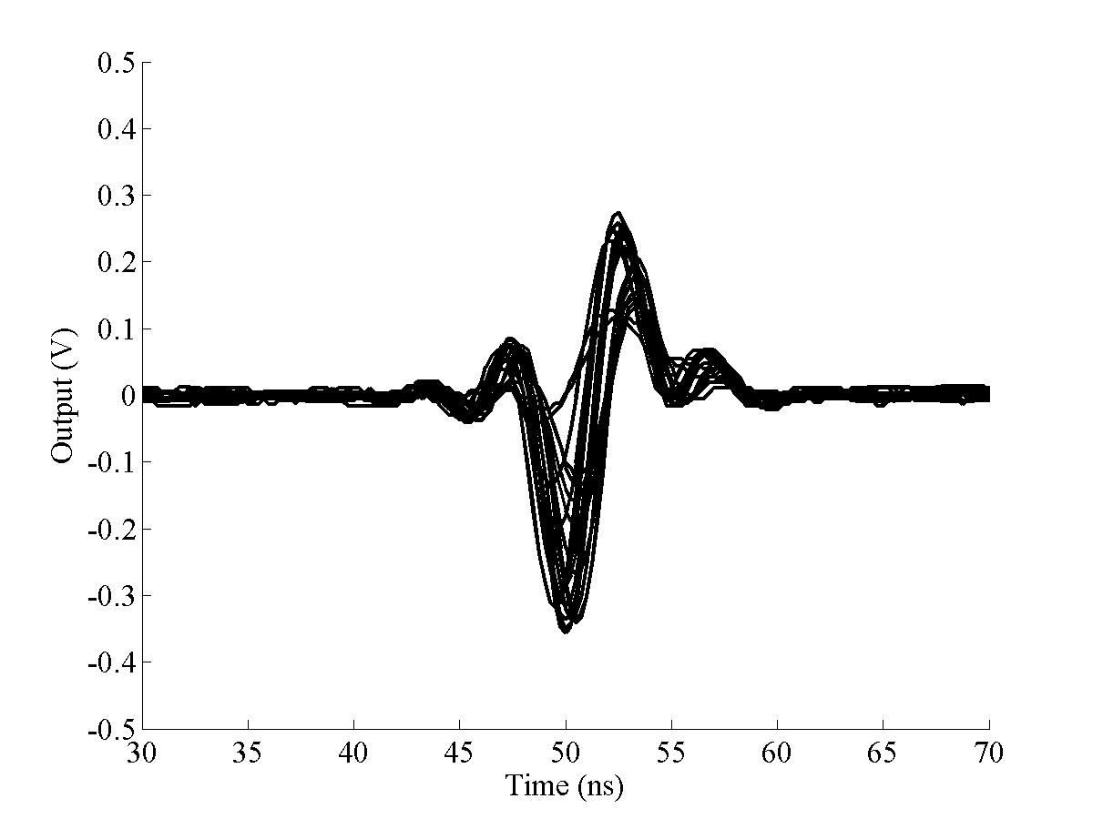
|
||||
| (c) 1.29 G-m | (d) 1.29 G-m | ||||
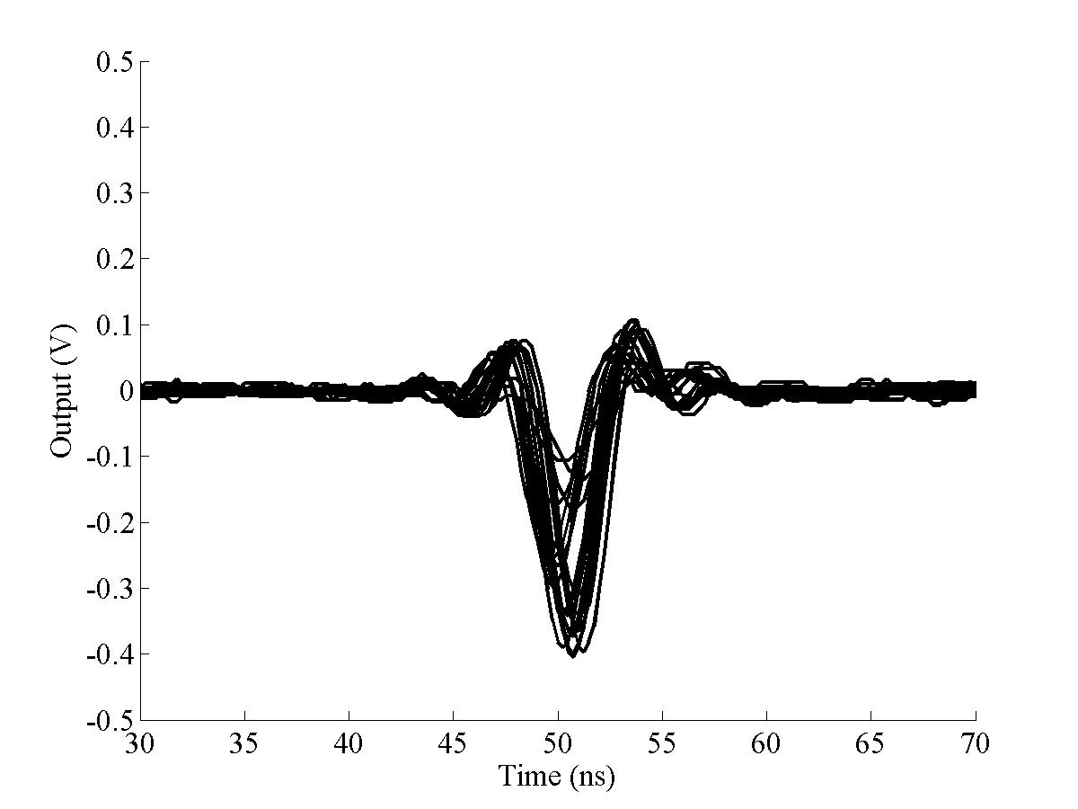
|
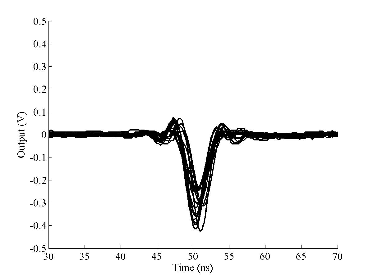
|
||||
| (e) −0.5 G-m | (f) −2.0 G-m | ||||
| |||||
| Figure 4.37: Normalised FONT BPM position vs. BPM 1761 position for 20 beam pulses at 35 different magnet settings. Normalised position is the max − min signal divided by the mean of the corresponding sum signal. The red line is a line of best fit produced through a χ2 minimisation. |
| Figure 4.38: BPM 1761 y position as a function of the integrated field, in G-m, of YCOR 1650 for 20 beam pulses at 35 different magnet settings. ‘BACT’ is the ‘actual’ integrated magnetic field, as calculated from the measured current in the magnet. The red line is a line of best fit produced through a χ2 minimisation. |
However, even though the BPM does not produce an expected position signal, it does appear to produce a response that varies with position. This can be seen in Fig. 4.36: this figure shows the variation of the BPM difference signal as a function of the integrated field, B.dL (in Gauss-metres), of YCOR 1650. An increasing field strength of YCOR 1650 corresponds to the beam being steered upwards: the beam is at its lowest at the FONT BPM for B.dL = −2.0 G-m and at its highest for B.dL = 4.0 G-m. If the BPM were performing in an ideal way, the profile for each pulse should follow the shape of the sum signal (Fig. 4.34), with a magnitude proportional to the beam position i.e. a positive peak for a beam high of centre and a negative peak for a beam low of centre. It would initially appear that, for each of the beam pulses shown in Fig. 4.33, there is no such correspondence between beam position and pulse magnitude, primarily due to the double peak that appears in the centre of most of the pulses. However, closer inspection reveals that the relative height of the two central peaks (one positive, one negative) does show an approximate dependence on the magnet field strength. By taking the difference between these two peaks (i.e. max − min), an approximate correspondence is observed between the FONT BPM signal and the measured beam position.
The y position measured by BPM 1761 is shown plotted against the normalised position for the FONT BPM in Fig. 4.37 for 20 pulses at 35 different magnet strengths: the normalised position is produced by dividing the max − min signal, for each pulse, by the mean value of the sum signal over the length of the pulse, in an approximation of the Δ/Σ method. This plot should be compared to Fig. 4.38, which shows the variation in vertical beam position, as measured by BPM 1761, as a function of the integrated field strength of YCOR 1650. Fig. 4.38 clearly shows that there is a smooth linear relationship between the variation of dipole field strength and the measured beam position downstream of that magnet: this is exactly what one would expect, given that there are no magnetic elements between YCOR 1650 and BPM 1761 (see Fig. 4.32). Due to the short pulse length, the position as measured by the stripline BPM can be taken as a good measurement of actual beam position, not only at BPM 1761 but also at the FONT BPM just upstream47. As such, Fig. 4.37 shows that, although the FONT BPM performs considerably less well than the stripline, it does respond to some degree to the actual position of the beam. Although the large spread in the normalised position of the FONT BPM is a significant fraction of the full measured range — 0.4 normalised units spread for a full range of 1.4 normalised units — there is still a clear trend that follows the line of best fit.
| Figure 4.39: The sum signal of the X-band BPM as a function of the toroid output for 700 pulses with the short pulse beam. Both signals are calculated using the peak value of each pulse. |
Fig. 4.37 also shows that the electrical centres of the FONT BPM and BPM 1761 are closely matched, since the fitted line passes very close to (0,0). However, it is also apparent when comparing Fig. 4.37 to Fig. 4.38 that the signal noise that appears on the normalised X-band BPM signal is not a result of actual jitter on the beam, since the position as measured by BPM 1761 shows an r.m.s. vertical beam jitter of ~70 µm: this is much less than the full range of 5 mm. The jitter on the X-band BPM normalised position measurement is some 20 times larger than that of the stripline BPM and is therefore likely to be a result of poor measurement by the X-band BPM, rather than true beam jitter. Another example of the poor short pulse performance of the FONT BPM is shown in Fig. 4.39. The peak output of the FONT BPM sum signal is plotted against the peak output of the toroid for each pulse. Given that both of these methods should give accurate measurements of the bunch charge of the beam, the distribution that appears in Fig. 4.39 is alarming: the expected positive linear relationship between two devices measuring the same quantity is clearly absent. No satisfactory explanation for this behaviour has yet been put forward. It is clear, however, that the X-band BPM behaves poorly in response to the short pulse beam.
As mentioned in the previous section, the double peak (henceforth referred to as “overshoot”) that appears on the BPM difference signal (Fig. 4.33) was unexpected: due to the sharpness of this peak and the relative variation of the sizes of the positive and negative peaks with beam position, as shown in Fig. 4.36, it is unlikely that this peak is a feature of the beam itself. The likelihood is that this overshoot is due to the BPM processor, with the following possible explanations:
A third possible option was that the phase slew across the pulse was causing the overshoot. As observed with the phase setting procedure, there is approximately a 20° phase slew over the length of the pulse. If the centre of such a signal was 90° out of phase with the reference signal, then the result of mixing two such signals together would produce a signal with zero output at this 90° point. The sign of the signal would then be positive before and negative after this 90° point if the reference signal was 90° ahead of the beam signal; the opposite would be true if the reference signal was 90° behind. However, the phase difference between reference and difference signals was only about 10° (see Section 4.6.2). Therefore, such an effect would not be noticeable, since the phase difference between the difference and X-band reference signals was set to be no more than 20°.
| Figure 4.40: RC-filtered Gaussian pulse used to simulate bunch train for short pulse beam. |
| Figure 4.41: Two RC-filtered Gaussian pulses, used to simulate the short pulse response for the top and bottom pickoffs with a 132 ps delay between pickoff signals. The top pickoff is shown in blue, with the delayed bottom pickoff shown in red. |
In an attempt to diagnose the cause of the problem from the two remaining possibilities, the various BPM signals input to and produced by the BPM processor were simulated in Matlab. The first task was to correctly simulate the pulse output by the BPM in response to the short pulse beam. In order to produce this beam pulse, the RC-filtered Gaussian pulse that was previously generated as part of the characterisation of the BPM response was used (see Section 4.5.2). The fitted parameters shown in Fig. 4.24 were used to produce the simulated pulse of Fig. 4.40. This pulse shape — simulating a Gaussian distribution of charge along the length of the bunch train — was considered to be a better approximation than that produced by the RC-filtered square pulse when compared to the real BPM sum signal data shown in Fig. 4.34. The Gaussian pulse shape was then used to modulate an 11.424 GHz signal to produce a facsimile of the real X-band output of each pickoff in response to the beam.
| Figure 4.42: X-band signal modulated with two RC-filtered Gaussian pulses, used to simulate the short pulse response for the top and bottom pickoffs with a 132 ps delay between pickoff signals. The top pickoff is shown in blue, with the delayed bottom pickoff shown in red. |
| Figure 4.43: The leading edges of the signals shown in Fig. 4.42: note the magnitude difference between the two pulses corresponding to the 132 ps delay. The top pickoff is shown in blue, with the delayed bottom pickoff shown in red. |
| Figure 4.44: The simulated X-band signal produced by adding the two pulses shown in Fig. 4.42: the phase of this signal contains the information on whether the resulting downmixed pulse will be positive or negative. |
The initial hypothesis was that an extra delay of 88 ps — one cycle of X-band — was causing the overshoot seen in the BPM difference signal. Two identical pulses were therefore created, as described above, in order to simulate the signal produced by the top and bottom pickoffs in response to the short pulse beam. They were then used to modulate an X-band signal to produce the true X-band output of each pickoff. The signal representing the bottom pickoff was then delayed by 132 ps with respect to the top signal: this is a delay of 1-1/2 cycles of X-band, corresponding to a 180° phase delay plus an extra cycle of delay introduced erroneously. The simulated pulse envelopes are shown in Fig. 4.41, with the resulting X-band signals shown in Fig. 4.42. An enhancement of the first 2 ns of Fig. 4.42 is shown in Fig. 4.43: note that the blue trace corresponding to the top pickoff signal can be seen to rise earlier than the red trace (bottom pickoff) as a result of the 132 ps delay in the bottom pickoff signal introduced into the simulation. The next stage in the processor is to subtract these two signals produced by the BPM pickoffs: this is achieved by adding the two signals, through a splitter/combiner (see Section 4.6 and Fig. 4.28), and produces the signal shown in Fig. 4.44.
| Figure 4.45: The simulated downmixed X-band signal produced by mixing the pulse shown in Fig. 4.44 with an X-band reference signal and low pass filtering the resulting output. The DC component, output by the mixer, is shown overlaid in black: this is the difference signal output by the FONT BPM processor. Note the similarity to the measured difference signal shown in Fig. 4.33. |
After subtracting the two raw pickoff signals to produce a difference signal at X-band, the final processor stage is to mix this difference signal at 11.424 GHz and low-pass filter it to recover the DC component. The mixed signal is produced by multiplying the difference signal with a reference signal at 11.424 GHz: the phase of this reference signal is crucial, since it must be exactly in phase with the original beam pulse. In terms of the simulation, this means that the reference signal is exactly in phase with the modulated X-band signal used for the top pickoff. The resulting signal is a convolution of the sum and difference frequencies (see Eq. (3.11)): as before, the DC difference frequency is the signal of interest; the 22.848 GHz sum frequency is removed by low pass filtering. The low pass filter used for the simulations was a 4-pole Bessel filter with fc = 200 MHz, as is used for the real BPM processor. The downmixed signal is shown in Fig. 4.45: the mixed signal is shown in red, with the filtered DC component shown in black. Note that this signal is surprisingly similar to the true FONT BPM difference signal shown in Fig. 4.33, but with the peaks reversed. The reason for this peak reversal is that, in the simulation, the signal from the bottom pickoff arrives later than that from the top pickoff; in the real processor it is the other way round (see Fig. 4.28).
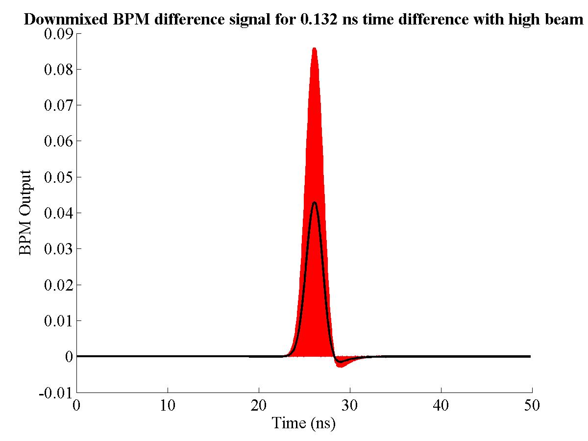
|
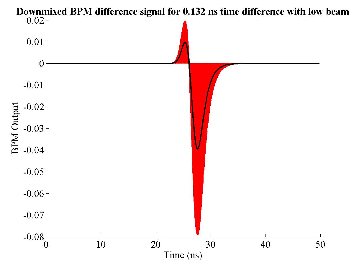
|
||||
| (a) High beam | (b) Low beam | ||||
|
|||||
In addition to the centred beam, both a high and low beam were simulated by increasing the magnitude of one of the signals shown in Fig. 4.41 with respect to the other by 10%. No attempt was made to ascertain the actual signal ratios for a particular beam position; it was not anticipated, however, that this would cause any problems with the realism of the simulation48. The simulated response for an off-centre beam is shown in Fig. 4.46: again, note the similarity between these simulations and the actual difference signal shown in Fig. 4.36. Although in each case one of the two peaks shrinks noticeably — the positive peak for a low beam and the negative peak for the high beam — it is still present in each case. This ‘peak shrinking’ can also be seen in the real difference signal for the various beam positions shown in Fig. 4.36.
| Figure 4.47: The simulated downmixed X-band signal produced for the ideal time delay between pickoffs of 44 ps; the DC component, output by the mixer, is shown overlaid in black. Note the similarity to the measured difference signal shown in Fig. 4.33. |
Having simulated the beam for an 88 ps error in the relative signal paths of the two pickoffs, the next step is to compare this result to the X-band BPM output for the correct signal delays. The simulation proceeds in the same way as described above, but with a relative delay between the two pickoffs of 44 ps rather than 132 ps. This 44 ps delay is used to turn the addition of the two signals into a subtraction at X-band, as described previously. The simulated downmixed difference signal for a 44 ps signal delay is shown in Fig. 4.47. Note that the signal shape in Fig. 4.47 is almost identical to that shown in Fig. 4.45. The only obvious difference between the two figures is the magnitude of each of the two peaks in both figures, which are noticeably larger for the longer time delay shown in Fig. 4.45: the output signal, shown in black, for the 44 ps delay of Fig. 4.47 is around 7.5 mV, about a third of the magnitude of the same signal in Fig. 4.45 at 22 mV. This point is crucial: the implication is that, for a perfectly functioning X-band BPM, the electronics will still produce the double peaked signal seen in Fig. 4.33. Even as small a difference in signal path as 44 ps makes the difference between an exact cancellation with a centred beam and the large peaks resulting from an inexact cancellation that appear in the real signals. This surprising result is due to the nature of the difference-over-sum procedure, where one takes a very small difference of very large signals: the very small time difference produces the same small signal difference, but due to the large raw signals produced by each pickoff this inexact cancellation produces the enormous double peaks seen in Fig. 4.33. The implication is that this will also be true for the long pulse beam: a description of the simulation as applied to the long pulse beam is given in Section 4.8.3.
| Figure 4.48: The simulated downmixed X-band signal produced for a relative phase error between pickoff signals of 10°. The DC component is shown overlaid in black: note that it is essentially zero for the entire pulse. |
In addition to the signal path difference, a phase error was also introduced to the simulation to test the effect of a phase difference between the two signal paths of the top and bottom pickoffs, resulting from an incorrect setting on one of the phase shifters. The simulation was identical to that previously described, but with a 10° phase difference introduced between the two signals corresponding to the two pickoffs, rather than a 44 ps time difference (a 10° phase error between the reference and difference signals was measured in Section 4.6.2). The simulation was therefore slightly artificial in the sense that any time delay between the pickoffs, necessary in the real system to enable signal cancellation by addition, was removed to try and isolate the effect of the phase difference. The result of this simulation is shown in Fig. 4.48: again, the mixed signal is shown in red, with the downmixed DC component shown in black. It is clear to see that the DC component is essentially zero, demonstrating that the cause of the BPM overshoot is not a result of the phase difference between pickoffs.
The conclusion is that the true cause of the BPM overshoot, or double peak, is the necessary 44 ps delay introduced into the processor to enable signal cancellation at X-band. It is therefore possible to refute the initial claim that this time difference would make no difference to the resulting downmixed signal (see above). Given the timescales involved, and comparing this time delay to the fitted time constant of the BPM of 1.5 ns (see Section 4.5.2), it is indeed surprising that such a small time delay should make a difference. It is an interesting question as to the point at which a relative time delay in the raw BPM pickoff signals no longer becomes important: clearly, on the basis of these simulations, the delay must be substantially more than two orders of magnitude smaller than the time response of the BPM pickoff before it becomes negligible.
Although the attempts to measure the position of the short pulse beam, as detailed in the previous section, were largely unsuccessful, a true test of the performance of the FONT BPM would be in response to the long pulse beam. The maximum pulse length available at the NLCTA is on the order of 180 ns, being the maximum portion of the X-band pulse used to drive the structures that is capable of stable beam acceleration. The maximum usable pulse length is on the order of 170 ns; the pulse length of the gun itself is around 220 ns. Although a much better response was expected from the FONT BPM in response to the long pulse beam, the associated disadvantage was that the position measurement of the NLCTA striplines would be much less reliable. Since the rise time of the long pulse beam is much longer than that of the short pulse beam, only those pulses which rise particularly quickly will register with the striplines, for reasons explained in Section 4.7. However, the advantage of the long pulse beam is that a much more reliable output is obtained from the toroid. For the short pulse, the ringing that appears at the end of the pulse (see Fig. 4.35) dominates; for the longer timescales associated with the 170 ns beam such ringing should be of minor significance.
| Figure 4.49: The raw output of the BPM processor sum signal (blue) and toroid output (red) for the long pulse beam; beam pulse is approximately 160 ns long. |
| Figure 4.50: The BPM processor sum signal (blue) and toroid output (red) for the long pulse beam. The toroid signal is scaled up by a factor of five to show the close profile match with the sum signal. Data is the same as that shown in Fig. 4.49. |
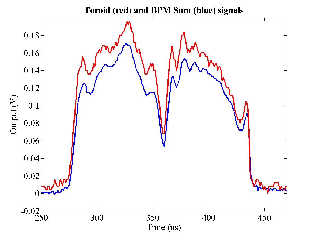
|
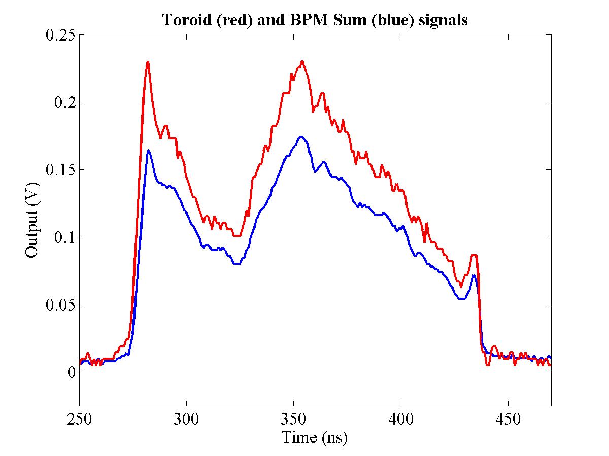
|
||||
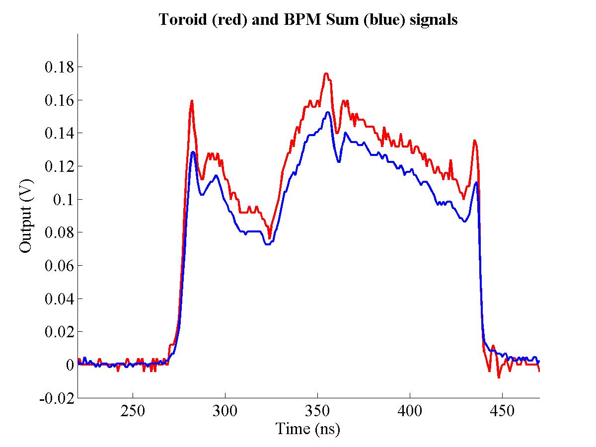
|
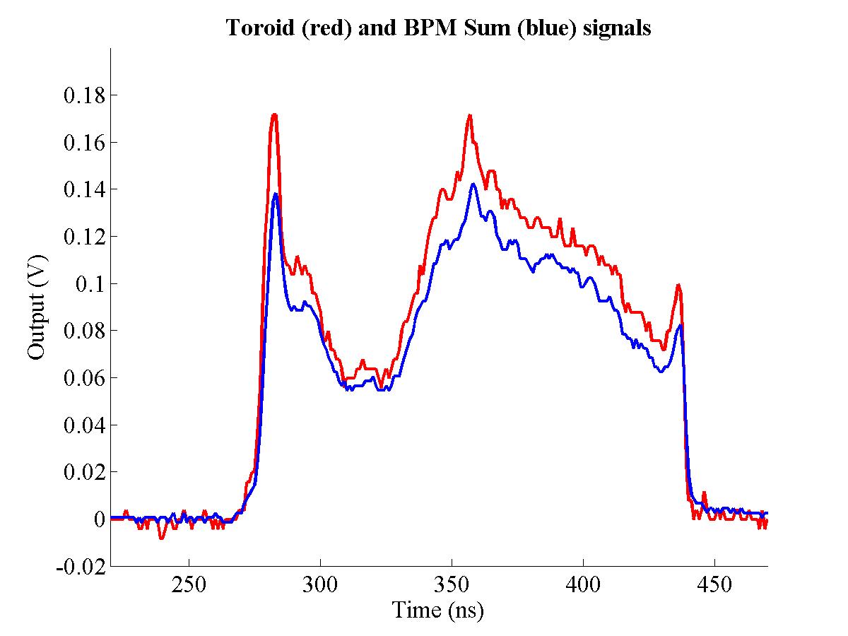
|
||||
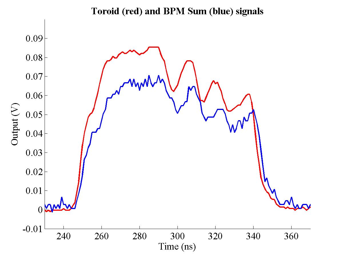
|
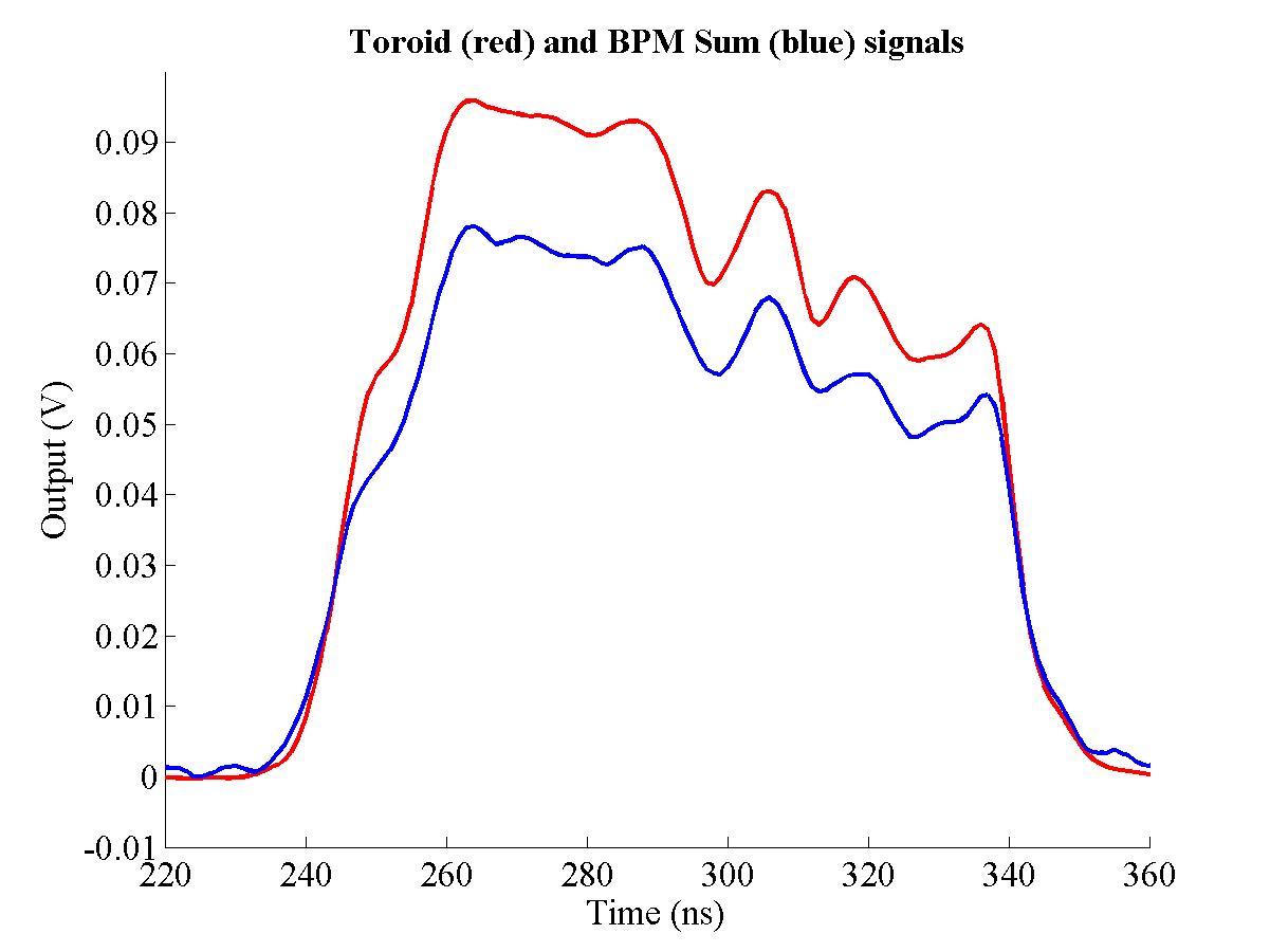
|
||||
| |||||
As described previously, the BPM processor sum signal should be an accurate representation of the beam charge. The long pulse response of the sum signal, along with the toroid, is shown in Fig. 4.49. The output of the BPM processor sum signal, shown in blue, is considerably larger than the toroid: this is due to the enhanced beam coupling of the X-band BPM to the beam as a result of its resonant behaviour. A modified version of this figure is shown Fig. 4.50, in which the toroid signal is scaled by a factor of five to match the magnitude of the BPM sum signal. The toroid is considered to be an accurate measure of the beam charge for the whole train: note that the two curves follow one another very closely. All of the features that appear on the toroid signal are clearly replicated on the sum signal. Another demonstration of the close match of these two beam charge measurement methods can be seen in Fig. 4.51. 6 different pulses are shown, each taken on different occasions: note the difference in pulse shape between each of the plots. It is clear on this evidence that the BPM sum signal is, as mentioned previously, as good a measure of the beam charge as the toroid.
This charge comparison can be taken a stage further by looking at the total charge measured for each pulse through both methods. By taking the mean signal value for each pulse, it is possible to compare the total charge measured through each method: this is shown in Fig. 4.52. In this figure, the mean BPM sum signal is plotted against the mean toroid signal for each of 130 consecutive pulses. The average signal value is taken between 210 and 370 ns (see Fig. 4.49): the limits are chosen to be wider than the pulse to ensure that the signal has settled sufficiently. Since the two methods are measuring the same quantity, one would expect a fit to the data to pass through zero: this can clearly be seen in Fig. 4.52 with the line of best fit. A χ2 minimisation was used to make a linear fit to the data, showing the expected one-to-one correspondence between the toroid and sum signal charge measurements. As such, contrary to the short pulse data the BPM sum signal is an excellent charge measurement for the long pulse beam. As noted in Section 4.5 the toroid has a coupling strength of 1.25 Volts per Amp of beam current [98]. Using the data shown in Fig. 4.52, the fitted gradient is 3.84, giving a coupling strength of 4.80 Volts per Amp of beam current for the BPM sum signal.
| Figure 4.52: The mean BPM processor sum signal vs. the mean toroid output for 150 pulses of the long pulse beam. The line of best fit (red) is produced using a χ2 minimisation; note that the fitted line has its origin very close to zero, indicating the excellent match between toroid and sum signal. |
| Figure 4.53: The BPM processor sum (blue) and difference (black) signals for the long pulse beam. Each trace is the average of 10 pulses; note that the difference signal has a similar shape to the sum signal, due to the beam charge density. |
| Figure 4.54: The normalised BPM output for the long pulse beam. The normalised output is produced by dividing the difference signal by the sum signal. The black line marks zero and the red lines mark the start and end of the pulse (see Fig. 4.53). The noise at the start and end of the pulse is due to the division of two very small signals (see main text). The trace is the average of 10 pulses. |
Having demonstrated that the BPM processor sum signal is an accurate measurement of the charge profile of a bunch train, the next stage is to examine the difference signal, in order to show that the Δ/Σ normalisation is effective when applied to the X-band BPM. An example of the BPM processor difference signal is shown in Fig. 4.53, with the sum signal from the same pulse for comparison. Since the difference signal is a convolution of both position and charge, it is clear to see that it has a similar shape to the sum signal. The normalised signal is produced by dividing the difference signal by the sum signal, and is shown in Fig. 4.54. The main part of the pulse (between the red lines) corresponds to the actual beam pulse. The noise that appears either side of this area is a result of the division process used for the normalisation: the signal here is very small for both sum and difference, so dividing one small number by another small number leaves one susceptible to small signal variations, which lead to the large variation seen. Unfortunately there is no method available at the NLCTA for corroborating the vertical beam position as measured by the FONT BPM. However, using the basic assumption that the beam should be approximately straight gives a guide as to the quality of the FONT BPM data. Although the normalised signal produced is approximately flat, it is unclear whether the slope that appears at the start of the pulse is a genuine beam effect, an artefact of the BPM response in combination with the BPM processor or a result of the normalisation process. There are also a number of features, such as the sharp rise at the start of the pulse, that correspond to features on the charge profile (see Fig. 4.53): these are dealt with in greater detail in Section 4.8.3.
| Figure 4.55: The normalised BPM output for the long pulse beam for 13 different beam positions. The horizontal black line marks zero and the vertical black lines the start and end of the pulse. The noise at the start and end of the pulse is due to the division of two very small signals (see main text). Each trace is the average of 10 pulses. |
| Figure 4.56: The normalised BPM output for the long pulse beam as a function of the integrated field of YCOR 1650. 13 beam positions were recorded, with 10 beam pulses at each position. The red line is a line of best fit produced through a χ2 minimisation. |
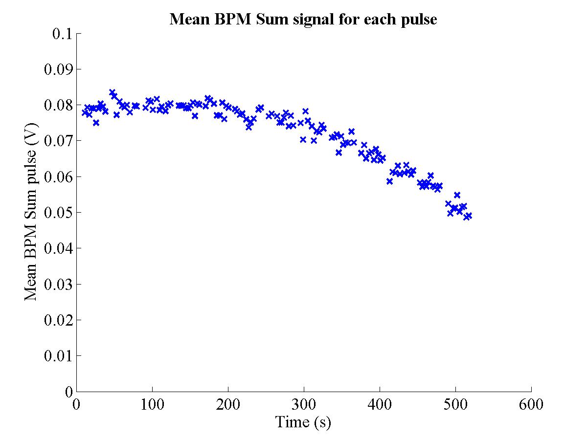
|
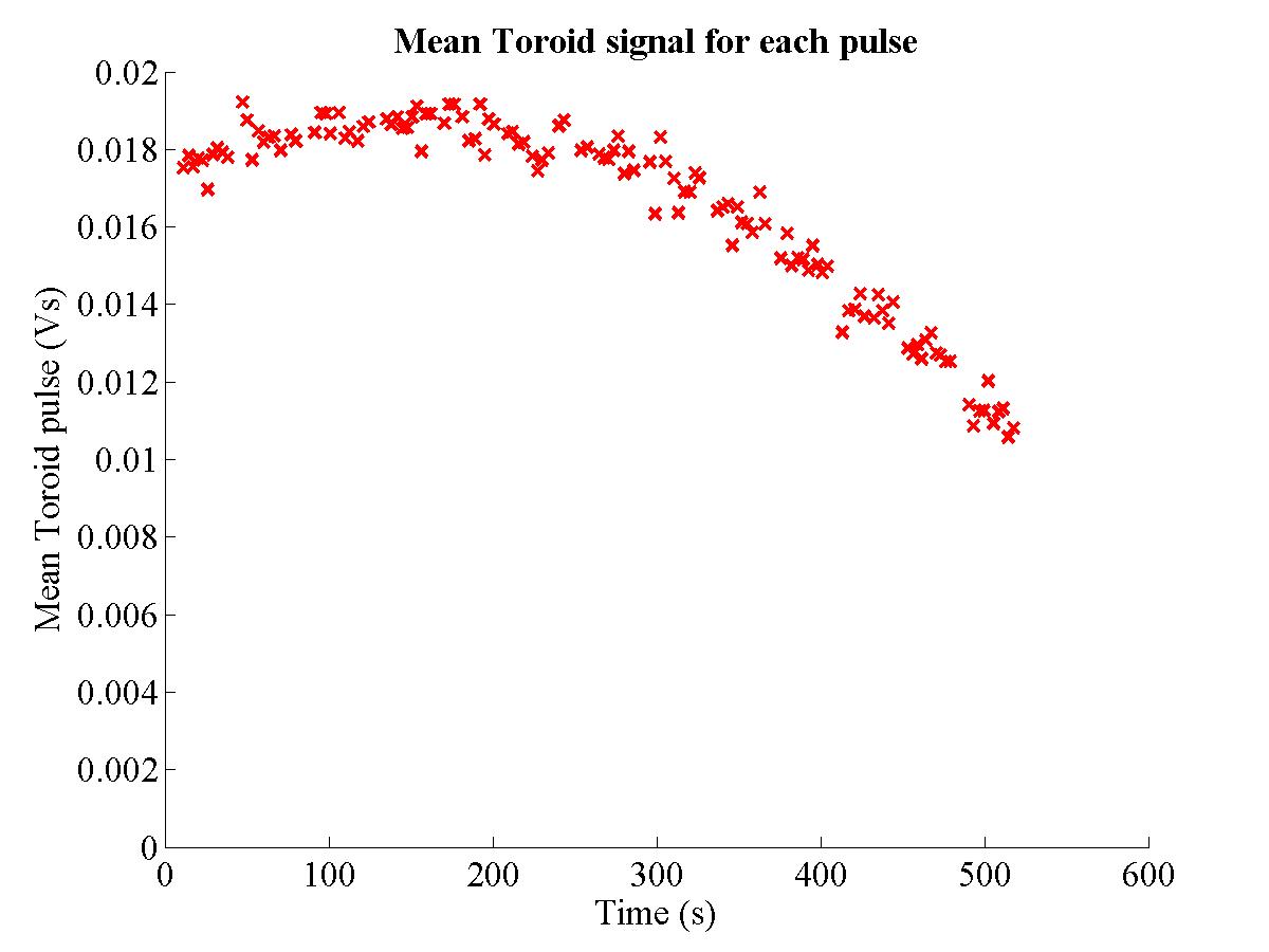
|
||||
| (a) Mean sum signal | (b) Mean toroid output | ||||
| |||||
In an attempt to measure the quality of the position measurement of the FONT BPM for the long pulse, the SCP was set up to steer the beam with dipole YCOR 1650 (see Fig. 4.32). 10 beam pulses were recorded for 13 field settings of YCOR 1650, with a variation between settings of 0.5 G-m. Both the integrated dipole field and the position measurement of stripline BPM 1761 were recorded. The resulting normalised beam positions are shown in Fig. 4.55. It is obvious at first glance that the pulse shape is repeatable from pulse to pulse: it also provides more evidence that the performance of the BPM processor is sound49. In order to correlate the normalised beam position with the dipole field, the mean of each pulse was taken between 320 ns and 440 ns: this is the region in which the pulse was considered to be stable and repeatable. A plot of the mean normalised position vs. the integrated field of YCOR 1650 for each pulse can be seen in Fig. 4.56. The position response shown in this figure is clearly an improvement over the short pulse position response (Fig. 4.37).
| Figure 4.58: The normalised BPM output for the long pulse beam as a function of the integrated field of YCOR 1650, using the first 8 dipole settings shown in Fig. 4.56. The red line is a line of best fit produced through a χ2 minimisation. |
It would appear from this plot that the normalised FONT BPM output has a nonlinear response to beam position, since it deviates above the line of best fit in the centre and falls below it towards either end. However, the larger integrated field of the dipole, and the associated normalised position measurement, correspond to a rapid fall off of the beam charge, as can be seen in Fig. 4.57. This figure shows the variation of the beam charge as a function of the time at which the measurement was made: note that there is a rapid deterioration in the beam charge after 300 s. This deterioration could be a result of the beam scraping on the aperture of the FONT BPM, the slope of the curve corresponding to the size of the aperture50. It could also be a result of the general deterioration in the quality of the beam. When the length of the long pulse beam was extended beyond ~150 ns, it was repeatedly observed to remain stable only for about 3 minutes before starting to deteriorate. If Fig. 4.56 is re-plotted with just the earlier data (corresponding to the first 8 dipole settings), a much better fit is obtained: this is shown in Fig. 4.58. The fit is clearly better than that shown in Fig. 4.56 as a result of using the high beam charge data. From this figure, a variation in normalised FONT BPM position of 0.323 normalised units (BPM units) per Gauss-metre of YCOR 1650 integrated dipole current is obtained.
| Figure 4.59: The normalised BPM output for the long pulse beam vs. the position measured by stripline BPM 1761. 13 beam positions were recorded, with 10 beam pulses at each position. The red line is a line of best fit produced through a χ2 minimisation. |
| Figure 4.60: The beam position measured by NLCTA stripline BPM 1761 as a function of the integrated field of dipole YCOR 1650. 13 beam positions were recorded, with 10 beam pulses at each position. The red line is a line of best fit produced through a χ2 minimisation. |
The final stage in measuring the position response of the FONT BPM to the long pulse beam is to compare the position as measured by stripline BPM 1761 to the normalised FONT BPM position. The beam position measured by BPM 1761 is shown plotted against the normalised FONT BPM position in Fig. 4.59. As one would expect, given the response shown in Fig. 4.58, the correlation between the two is again linear, to a good approximation. Again some nonlinear behaviour is evident further away from the centre of the beampipe. However, by comparing this plot to Fig. 4.60, which shows the response of BPM 1761 as a function of the integrated field of YCOR 1650, it is likely that the main source of this nonlinearity is the stripline BPM response. The data in Fig. 4.60 shows the same ‘S-bend’ shape as that in Fig. 4.59: since this is not present in Fig. 4.58, it is probable that this is a result of the stripline BPM response and not the X-band BPM. It is therefore likely that the X-band BPM has a long pulse position response that is very close to linear, for a beam that is close to its electrical centre.
By examining the data in Fig. 4.59, it is possible to relate the normalised position variation of the FONT BPM to the actual position variation as measured by stripline BPM 1761: a normalised position of 0.299 ± 0.012 BPM units = 1 mm for the fit to the data in Fig. 4.6051. It is also possible to put an upper limit on the precision of the normalised position measurement from the r.m.s. spread on each position. Since this position spread is likely to be dominated by beam jitter, rather than the precision of either BPM, the lowest r.m.s. position variation for each dipole setting is used. The minimum r.m.s. jitter on the stripline position is 22 microns (for the positions measured at~1 mm offset). The corresponding minimum jitter for the FONT BPM normalised position is 0.0069 BPM units which, using the previously measured scale for the normalised position variation corresponds to an r.m.s. jitter of 23 microns. Note that both these values are smaller than the previously measured beam jitter shown in Fig. 3.26. Given the sensitivity of the beam variation over a timescale of minutes, as noted above, it is likely that the beam jitter is closely related to the beam quality.
In Section 4.7.2, an explanation was given for the double peaked signal overshoot that appears on the difference signal for the short pulse beam. The implication is that such an effect should also be seen to some degree in the long pulse beam response. Although it is unclear from the data presented in Section 4.8.2, a clear example of this signal overshoot was observed on the difference signal for a number of sets of data. One example of such a signal is shown in Fig. 4.61, with the accompanying toroid signal in Fig. 4.62. Note that, at around 60 ns into the pulse the charge drops sharply on the toroid output. A corresponding drop is apparent on the X-band BPM difference signal, but instead of getting close to zero and then rising again, the BPM signal actually crosses over zero, becoming positive, before returning to its large negative value. A similar overshoot appears at the end of the pulse around 120 ns. The hypothesis was that the cause of the double peaks in the short pulse data was also the cause of the overshoots that one sees in the long pulse data i.e. that the incorrect cancellation occurring from the time difference in the signal paths causes the X-band BPM signal to overshoot.
| Figure 4.61: The BPM difference signal for a single pulse of the long pulse beam. Note the overshoot that appears at 60 ns and 120 ns as a result of the inexact signal cancellation. |
| Figure 4.62: The output of the toroid for the same pulse shown in Fig. 4.61. Note the location of the dips in the charge profile at 60 ns and 120 ns. |
| Figure 4.63: The simulated X-band BPM raw pickoff signals used to simulate the difference signal shown in Fig. 4.61. The blue trace represents the top pickoff signal and the red trace the bottom pickoff signal; relative time delay between signals is 0.5 ns. |
| Figure 4.64: The simulated X-band BPM difference signal using the two pulses shown in Fig. 4.63. Note the similarity to the actual difference signal shown in Fig. 4.61. |
To produce a facsimile of the actual pulse that arrives at the X-band BPM electronics, one of the recorded toroid signals was used to replicate the pickoff signals. Due to the relatively coarse granularity of the pulse as a result of the finite sampling rate of the scope, the bottom pulse was delayed in relation to the top pulse by some 0.5 ns; as before, the magnitude of the bottom signal was increased by 10% to simulate a beam off-centre (for comparison with the data). Again, these figures probably reflect some modicum of realism: although 0.5 ns is ten times longer a delay than one sees with a single half cycle delay at X-band (the actual figure is probably, given the relative signal path lengths of the processor used at the time, in the region of two and a half cycles, or 220 ps) the general effect of introducing a delay should still stand. As before, the signals were multiplied with an 11.424 GHz signal, subtracted and downmixed to DC with another 11.424 GHz signal; the raw signals can be seen in Fig. 4.63. The resulting signal is shown in Fig. 4.64: this shows the simulated position signal produced using the aforementioned cancellation method. There is a clear similarity between this pulse shape and the true X-band BPM difference signal shown in Fig. 4.63: instead of dropping towards zero without overshooting, which is the case for the charge signals used as the signal source for this output, the simulated signal overshoots past zero at similar points to that seen in the real data. It is also interesting that overshoots occur only in response to the falling edge of the charge signal, as mentioned above.
The likely conclusion is therefore that the cause of these overshoots is the signal path difference used for the signal cancellation, necessary to provide the difference signal used for the position measurement. Since these overshoots appear when the charge distribution of the beam drops rapidly, it is important that the beam have as flat a charge profile as possible. There is always a suspicion that, where a rapid change in normalised beam position is also accompanied by a rapid change in the beam charge, that this is a result of the same overshoot effect rather than a true change in beam position. Close inspection of Fig. 4.53 reveals that the first 70 ns of the sum signal shows a trough in the charge distribution. As expected, there is a corresponding trough in the difference signal: however, the trough in the difference signal is more pronounced than that of the sum signal, leading to a replication of this shape on the normalised signal (Fig. 4.54). The same is true for each sharp feature that appears on the sum signal: it is replicated on the difference signal, but appears sharper, and therefore reappears on the normalised signal. The likely explanation for this behaviour is the 44 ps signal path difference, as explained above. As a result, it was necessary to tune the beam very carefully for the FONT beam tests (Chapter 5) in order that the charge profile was as flat as possible. This was made all the more difficult by the rapid deterioration of the quality of the beam. For future iterations of the BPM processing electronics it is recommended that an alternative processing scheme is employed in order to eradicate this overshoot phenomenon.
As described in Section 3.5, an experimental test of the IP fast feedback system was considered crucial in proving the principle of a feedback system with a nanosecond scale time response. Although both the IPFB simulations (Section 3.4) and the bench tests of the BPM processor components (Section 3.3.3) give some degree of confidence that the true IPFB system should behave as predicted (see Section 3.2 and [58]), it was felt that a true experimental test of the electronics, incorporating some normalisation scheme (nominally the Δ/Σ scheme as used for the X-band BPM, as described in Section 4.6), and a method of high speed position correction of a real bunched beam was essential in demonstrating the effectiveness of the IPFB system. Such a test, given the name FONT (Feedback On Nanosecond Timescales), was realised on the NLCTA, as mentioned briefly in Section 3.5.2. The aim of the FONT experiment was to replicate the conditions of the NLC IP to allow a comprehensive test of the IPFB electronics.
A series of electronics was designed and constructed at SLAC and Oxford with this intention in mind. The key principle behind FONT was to be able to apply an iterative correction to an off-centre beam within a single bunch train. A number of options were considered for the main objective of the FONT experiment. However, that which was felt to most closely replicate the goals of the IPFB system was to centre the beam at a single BPM. In other words, a beam would be seen to be off-centre by a BPM and, through re-steering that beam based upon the measurement made by the BPM, set the BPM signal to zero. This is clearly not the same as steering a beam to a desired trajectory, as is the requirement for the real IPFB system. With just a single BPM, the FONT system has no knowledge of the angle, and hence the trajectory, since only a single position measurement can be made. However, this is essentially the same as the current design of the IPFB system: its only knowledge of its success is whether, as a result of the beam-beam interaction, the position at the BPM is set to zero. As such, it was felt that designing the electronics to this end would provide the best proof of principle of the IPFB system electronics.
The obvious disadvantage of using the NLCTA for a beam test of the IPFB system is that the accelerator has no IP. The feature that sets the IPFB system apart from other feedback systems is its use of the enormous beam-beam kick between the two colliding bunches to translate a nanometre-level offset at the IP into a micron-level position measurement at the IPFB BPM. Unfortunately, it is the beam-beam interaction that is the least well-known element of the entire IPFB system. However, since no nanometre colliding beam facilities exist on which one could build a test setup of the IPFB system, one is limited to using a single beam and modifying the experimental setup accordingly. The layout of the FONT experiment at the NLCTA and the replication of the beam-beam interaction are dealt with in Sections 5.1.1 and 5.1.2.
| Figure 5.1: The front section of the NLCTA, showing the gun, injector, chicane and one of the test structures. Figure adapted from [76]. |
| Figure 5.2: The rear section of the NLCTA, showing the diagnostic tools, the beam dump and the area used for the FONT experiment. The diagnostics include a toroid, a profile monitor and a large kicker used to measure the longitudinal beam profile and beam energy. The FONT area is marked in red, between quads QD1550 and QD1760. The FONT BPM is located at the downstream end, upstream of QD1760 and Toroid 1750. Figure adapted from [76]. |
The principle behind the FONT experiment was to try and make a rapid correction to a beam offset as measured by the FONT BPM. The offset would be introduced upstream of the BPM with a dipole and be measured by the FONT BPM. The signal from the BPM would then proceed through the IPFB electronics in the same way as the actual system (see Section 3.2.1). The raw BPM signal is processed using the Δ/Σ method; a high speed power amplifier is then used to drive a kicker to correct the measured beam offset. In this way, the FONT experiment would replicate the whole IPFB system. An important consideration when choosing the location of FONT on the NLCTA was the anticipated latency of the system. It was crucial to be able to match the round trip delay of FONT with that of the real IPFB system: this is the reason for FONT taking up some 4 m of the NLCTA beamline. The total beam flight distance, for the IPFB system in its current location (see Fig. 3.3), is some 8 m, with only a few centimetres of cable length used to connect the BPM processor to the kicker amplifier. For FONT, using 4 m of beamline gives the same round trip distance, since the processed BPM signal must be transmitted back upstream to the start of the FONT region where the beam offset and correction would be applied.
| Figure 5.3: Schematic diagram of the FONT region of the NLCTA, showing the various beamline components. A description of the FONT BPM is given in Chapter 4; the FONT magnet assembly is detailed in Section 5.2. Figure adapted from [76]. |
Changing the length of the beamline used for FONT would also change the requirements of the FONT electronics. Moving the BPM closer to the source of the beam offset would shorten the latency period, allowing greater scrutiny of the feedback electronics by increasing the number of latency periods for which FONT would operate. However, for the same angular deflection applied to the beam the BPM would register a smaller signal, requiring a larger gain in, and increasing the power requirements of, the kicker amplifier. Increasing the length of beamline used for FONT would have the opposite effect, decreasing the required kick while increasing the latency period. As such, a beam flight distance of 4 m was also considered optimum for the FONT electronics. There were also beam optics considerations in the location of FONT, which are detailed in the next section.
As stated in Section 3.5, the NLCTA is an entirely self contained accelerator, with its own gun, injector, chicane, accelerating structures and beam dump. A schematic diagram of the entire NLCTA can be seen in Figs. 5.1 and 5.2. Six sections of the accelerator were originally set aside for experimental X-band accelerator structures. Since only the first four of these sections of beampipe were used, FONT made use of the two remaining sections of beampipe, between quads QD1550 and QD1760: the FONT area is marked in red on Fig. 5.2. The FONT BPM, detailed extensively in Chapter 4, was installed upstream of QD1760 and Toroid 1750, as shown on Fig. 5.2; a close-up of the FONT area is shown in Fig. 5.3 (greater detail of the NLCTA stripline BPM's up and downstream of the FONT BPM location is shown on Fig. 4.32). The NLCTA beam parameters at this location are summarised in Table 3.3. As described in Section 4.3, the FONT BPM location was chosen to allow corroborative position and charge measurements to be made with stripline BPM 1760 and Toroid 1750. 4 m upstream of the FONT BPM resides QD1550 that marks the start of the FONT region.
In order to apply a deflection and correction to the beam, a method was required for creating a vertical position offset at the FONT BPM and correcting that offset. The simplest way of doing so was to steer the beam 4 m upstream of the BPM with a dipole magnet: the angular offset introduced by the dipole results in a position offset at the BPM. Having measured a position at the BPM, the FONT electronics would then transmit the corrective signal upstream to another magnet and remove the offset. These two magnets have very different requirements: the ‘offsetting’ magnet has no requirements for its response time, since one can dial in an offset well in advance of the beam. However, since it is essential to measure the repeatability of the FONT system, the long term stability of the magnet is crucial: any drift in the angular deflection applied to the beam reduces the quality of the data collected for FONT. The simplest solution was to use a standard SLC dipole magnet: details are given in Section 5.2.1. The ‘correcting’ magnet, on the other hand, must have a nanosecond level response time in order to provide a rapid correction to the beam. As such, a dipole magnet was not a realistic option. The magnet finally selected to provide the rapid position correction was a parallel plate electromagnetic kicker, similar in design to that of the real IPFB system (see Section 3.2.3); details of the magnet can be found in Section 5.2.3.
Having selected the two kinds of magnet required, the magnet arrangement had to be decided upon. From the point of view of the beam optics, the simplest option is to have both components at the same location. Normally this would not be possible, since both magnets take up a finite length of beamline: a close approximation is to have both components next to one another with nothing in between, since the position and angle difference between the two magnets is assumed to be zero over short distances. However, the magnet assembly for FONT was able to combine the two magnets into a single unit: this ensures that a particular angular deviation applied to the beam by each magnet results in exactly the same position change at the BPM. As such, there exists a direct comparison between the effect of both the ‘offsetting’ and ‘corrective’ magnets. The FONT magnet assembly is described in detail in Section 5.2.
| Figure 5.4: Horizontal and vertical beta functions for the NLCTA, generated with MAD using the design lattice [106]: βx is the solid line and βy the dashed line. The FONT area begins after QD1550, at 23 m, with the FONT BPM situated upstream of QD1760 at around 27.5 m, and is marked on the figure. Note that quadrupole QD1650, situated in the centre of the FONT region at 25 m, defocuses in y. |
The NLCTA beta functions were also a motivating factor for the location of FONT. A large vertical beta function corresponds to both a large vertical beam size and position jitter [30]. To maximise the deflection seen at the FONT BPM, it is desirable to locate it at a point in the lattice with a large vertical beta function. The horizontal and vertical beta functions for the design lattice of the NLCTA are shown in Fig. 5.4. The FONT magnets, located at ~23 m, and the FONT BPM, located at ~27.5 m, are both at locations with a large vertical beta function, maximising the effectiveness of the kick.
In addition, FONT makes use of the placement of quad QD1650, situated directly between the magnet assembly and the FONT BPM. From a beam transport perspective, the beamline location of FONT is extraordinarily simple: two drift spaces are separated by a quad, for which 3 transport matrices are required to calculate the effect of the quad on the kick applied to the beam by the FONT magnets. The two drift spaces are also of identical length, since the location of the FONT magnets and the BPM is symmetrical about QD1650: the total distance between the centre of the magnet assembly and the centre of the FONT BPM was 4.18 m. From Equations 2.14 and 2.16, the effect of this beamline arrangement on the vertical beam position and angle, y and y′, is described by the following matrix equation:
| (5.1) |
where L is the distance between the magnet assembly and the BPM, Kl is the integrated field strength of the quad and Bρ is the magnetic rigidity (see Section 2.2.1). The corresponding matrix equation without the quad is simply:
| (5.2) |
By examining the beta functions in Fig. 5.4, QD1650 actually defocuses in y and the factor Kl becomes positive in Eq. (5.1). As such, assuming that the beam arrives with no vertical offset at the FONT magnet assembly (i.e. ymagnets = 0) the vertical offset seen by the FONT BPM (yBPM) as a result of a deflection applied by the FONT magnets (y′magnets) is:
| (5.3) |
The kick applied to the beam by the FONT magnets is therefore enhanced by a factor
The magnet assembly is an integrated construction, consisting of the two magnet types mentioned briefly in the previous section. The full assembly can be seen in Fig. 5.5: the purpose of this integrated assembly is to combine the two FONT magnets into a single unit that steers the beam at exactly the same point. The dipole is a modified SLC Type 4 Corrector and is described in Section 5.2.1; the kicker is a standard SLC Scavenger Post Kicker Magnet, details of which are given in Section 5.2.3. The combined unit was installed in the NLCTA downstream of quad QD1550, as indicated in Fig. 5.3: a photograph of the installed magnet assembly is shown in Fig. 5.6. The construction and performance of each of the magnets is detailed in the rest of this section. Initially it was uncertain whether a separate dipole would be needed, or if it was simpler to take advantage of the dipole mode of the existing quadrupoles (namely QD1550) within the NLCTA. However, it was felt that the possibility of using a dipole that was independent of the NLCTA would give greater options for location and customisation: it would also allow the construction of the integrated magnet assembly already described.
| Figure 5.5: The FONT integrated magnet assembly. The dipole coils are red and mounted around the silver barrel of the kicker magnet. |
| Figure 5.6: The FONT integrated magnet assembly installed on the NLCTA. The assembly is mounted around a length of ceramic beampipe and is supported by two beamline support struts. The quad on the left of the picture is QD1550. |
| Figure 5.7: The SLC Type 4 Corrector magnet used in the construction of the FONT integrated magnet assembly. |
| Figure 5.8: A Schematic diagram of the SLC Type 4 Corrector. Measurements are in inches; figure adapted from [107]. |
The original construction of the SLC Type 4 Corrector is shown in Figs. 5.7 and 5.8 52. From Eq. (2.4) (see Section 2.2.1), the magnetic rigidity can be restated as:
| (5.4) |
for a momentum p in MeV. Using a small angle approximation (i.e. l = ρθ for a magnet of length l), the integrated field strength Bl, in kiloGauss-metres (kG-m), of a dipole required to steer a beam through an angle θ radians is given by:
| (5.5) |
The maximum range of beam positions measured at stripline BPM 1761 is ±4 mm: beyond this range, the beam scraping on the upstream aperture of the FONT BPM causes a large reduction in beam charge; the stripline response also becomes distinctly nonlinear (possibly as a result of this scraping). This corresponds to a maximum angular deflection at the FONT magnet assembly of 1 mrad. For the NLCTA beam energy of 62 MeV, this sets the maximum integrated field strength of the FONT dipole at 2 G-m. This places two constraints on the performance of the dipole:
The vertical beam jitter at the FONT BPM, as measured by stripline BPM 1761, is of the order of 40 microns (see Section 4.8.2 and Fig. 3.26). Since the stability of the field within a dipole is primarily dependent upon the current stability of the power supply, it is therefore necessary that the dipole power supply have a current stability of 1% within the current range required to produce the maximum dipole field. The simplest way of driving the FONT dipole was to make use of one of the existing corrector power supplies used to drive the vertical dipole of quad QD1550. In this way, the FONT dipole would be transparent to NLCTA operations, since the dipole of QD1550 is replaced with the FONT dipole just downstream (see Fig. 5.6). The power supply used to drive the correctors within the NLCTA is a 6 A Mk II 16 Channel Corrector Driver. With a maximum output of ±6 Amps, the power supply has a current stability better than 0.1% of maximum, or 6 mA, over a 24 hour period; it is also stable to much better than 0.1% over 10 minutes or so [108]. It is likely that the power supply is stable to 1% down to ~100 mA. As such, given the magnet range used for the measurements in Section 4.8.2, the full range of ±2 G-m should correspond to a power supply output of ±1 A.
|
||||||||||||||||||||||||||||||||||||||||||||||||||||
|
| Figure 5.9: The hysteresis curve for the Type 4 Corrector magnet, using the data shown in Table 5.1. |
Measurements were carried out on the Type 4 dipole to determine whether the magnet had the required current-field strength characteristics: these measurements are summarised in Table 5.1 [109]. The first feature to note is that the relationship between applied current and integrated field is nonlinear. This is a result of the hysteresis behaviour of the iron yoke around the dipole coils. Hysteresis arises as a result of the inherent magnetisation of all ferromagnetic solids. As such, for any ferromagnet the inherent magnetisation is not only a function of any applied magnetic field but also the previous state of magnetisation of the material, resulting in a nonlinear relationship between the applied field and inherent magnetisation [110]. The hysteresis curve resulting from the data in Table 5.1 is shown in Fig. 5.9. The purpose of the iron yoke is not only to provide a solid superstructure for the magnet coils, but also to increase the integrated field for a given current: the iron provides an easier return path for the magnetic field, meaning that less energy is required to sustain the field and leading to a higher field strength.
| Figure 5.10: Schematic diagram of the SLC Type 6 Corrector; note the yokeless design. Measurements are in inches; figure adapted from [111]. |
However, for the purposes of FONT the problems associated with the hysteresis behaviour of the magnet outweigh the advantages of the increased field strength, since a precisely, rather than approximately linear response is required. In fact, the addition of the iron yoke increases the integrated field strength above the threshold stated above: at its minimum value, a current of 1 A results in an integrated field of 7.3 G-m, significantly larger than the required field strength of 2 G-m per Amp. As a result of these measurements, the dipole's iron yoke was removed and a new support structure was designed. The construction of this dipole was based around another, smaller yokeless magnet used in the SLC, referred to as a Type 6 Corrector: a schematic diagram of this magnet is shown in Fig. 5.10. The design was modified to match the size of the coils and to expand the inner distance between the coils to 5 inches. The support structure was machined from G-10 plastic and assembled in the same way as the Type 6 Corrector: the new dipole can be seen mounted around the kicker magnet in Fig. 5.5. The new integrated field of the FONT dipole assembly was measured to be 15.50 G-m for a supply current of +6 A and 14.65 G-m at −6 A, giving an average integrated field strength of 2.51 G-m per Amp [109]. Therefore a current of 0.796 A is required to produce a field of 2 G-m, much closer to the field strength of 2 G-m/A as specified previously.
The FONT dipole was mounted tightly around the kicker magnet (details of the kicker are given in Section 5.2.3) to form an integrated unit and installed onto the NLCTA beamline, downstream of QD1550, at the same time as the FONT BPM. The installed magnet assembly with support structure is shown in Fig. 5.6. Two struts were used to support the magnet assembly, with the whole unit kept rigidly in position once it was mounted to the beampipe. The magnet was initially aligned by eye, at the time of installation, and later as part of a more rigorous NLCTA alignment procedure.
In order to measure the performance of the FONT dipole, the same procedure utilised for the FONT BPM response measurements, in Section 4.8.2, was used. Since the dipole was connected to the corrector power supply in place of the QD1550 y corrector (YCOR 1550), it could be programmed and controlled in the same fashion as any other dipole on the NLCTA. A correlation plot was set up with the SCP to record 10 beam pulses at 17 different magnet settings, using the long pulse beam. The SCP was programmed to step YCOR 1550 through 17 steps of 0.5 G-m; this range corresponds to the original 1550 y corrector, not the FONT dipole. The conversion factor required to give the field strength for the FONT dipole depends upon the gradient of each magnet: YCOR 1550 has a gradient of 6 G-m per Amp, 2.39 times larger than the gradient of 2.51 G-m per Amp for the FONT dipole53.
| Figure 5.11: The normalised BPM output for the long pulse beam as a function of the integrated field of the FONT dipole. The beam position of 10 beam pulses was recorded for 17 dipole settings. The red line is a line of best fit produced through a χ2 minimisation. |
| Figure 5.12: The beam position measured by NLCTA stripline BPM 1761 as a function of the integrated field of the FONT dipole. The beam position of 10 beam pulses was recorded for 17 dipole settings. The red line is a line of best fit produced through a χ2 minimisation. |
| Figure 5.13: The beam position measured by NLCTA stripline BPM 1761 as a function of the integrated field of the FONT dipole, using the central 8 dipole settings shown in Fig. 5.12. The red line is a line of best fit produced through a χ2 minimisation. |
As before, the FONT BPM position was normalised by dividing the difference signal by the sum signal: the normalised pulse was then averaged between 320 ns and 440 ns (cf. Fig. 4.54) to give a single normalised position output for each pulse. A plot of the normalised FONT BPM position as a function of the calculated field strength of the FONT dipole is shown in Fig. 5.11. This plot is equivalent to Fig. 4.56 which shows the normalised position as a function of the integrated field strength of YCOR 1650. Note that, once again, the variation in dipole field produces an approximately linear response in the BPM. A more rigorous test of the performance of the dipole is shown in Fig. 5.12: here the beam position measured by stripline 1761 is plotted as a function of the calculated field strength of the FONT dipole (cf. Fig. 4.60). As before, the stripline response has a slight nonlinear ‘S’ shape to its response curve. With the knowledge that a stripline BPM has a response that is most linear with a beam close to centre, the middle 8 beam positions are plotted in Fig. 5.13. For this range of values, it is clear that there is a linear relationship between the measured beam position and the integrated field strength of the FONT dipole. As such, it is possible to conclude that the FONT dipole is operating as one would expect. It is important to note that the only effect of the intervening quad, QD1650, is to amplify the angular deflection imparted to the beam by the FONT dipole, since the data in Fig. 5.13 shows no deviation from the expected linear response.
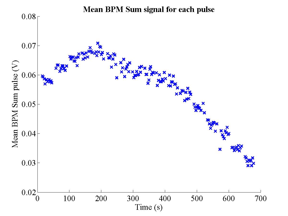
|
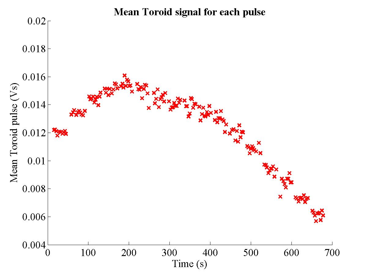
|
||||
| (a) Mean sum signal | (b) Mean Toroid output | ||||
|
|||||
It is now possible to compare the field strengths and performance of the FONT dipole to YCOR 1650. The integrated field strength of YCOR 1650 required to produce a 1 mm vertical deflection, as measured by BPM 1761, is 0.93 G-m (see Fig. 4.60). The corresponding figure for the FONT dipole, using Fig. 5.13, is 0.41 G-m. This is to be expected, since there is a larger distance between the FONT dipole and BPM 1761. However, if there was no quad between the dipole and BPM, one would expect the figure for YCOR 1650 to be twice that of the FONT dipole, since it is half the distance from BPM 1761. Therefore, the beam deflection of the FONT dipole is enhanced by a factor of 1.14: this compares favourably to the predicted enhancement of 1.09 from Eq. (5.3). Clearly this enhancement will increase for a greater quad field strength: it is a matter for further investigation to determine the optimum quad strength to maximise the enhancement while still keeping the beam jitter at the FONT BPM at a reasonable level.
Finally it is also possible to compare the FONT BPM/stripline position response curve for YCOR 1650, shown in Fig. 4.59, to that of the FONT dipole. As before, the central 8 positions are used to determine the linearity of the normalised position measurement. Not only is this the region in which the stripline BPM is most likely to be linear, it is also the range in which the beam charge (and hence the sum signal) is large enough to accurately calculate the normalised position. The charge measurement for the FONT dipole dataset is shown in Fig. 5.14 (cf. Fig. 4.57): note that, after ~400 s, the charge deteriorates significantly54. The normalised and measured stripline positions for each pulse are shown on Fig. 5.15 for the FONT dipole measurements. For YCOR 1650 the relationship 0.299 ± 0.012 BPM units = 1 mm was measured. The relationship for the FONT dipole dataset is 0.314 ± 0.011 BPM units = 1 mm (see footnote 51). The close match between these two measurements is another indication that the FONT BPM correctly measures beam position.
| Figure 5.16: The SLC Scavenger Post Kicker magnet used in the construction of the FONT integrated magnet assembly. The input connectors are covered by yellow protective caps, on the right hand end of the kicker barrel. |
| Figure 5.17: A Schematic diagram of the SLC Scavenger Post Kicker. The kicker plates are approximately 30 cm in length; measurements are in inches. Figure adapted from [112]. |
The kicker magnet used as the ‘corrective’ magnet for FONT was an SLC Scavenger Post stripline kicker. This type of magnet is used within the SLC Damping Rings to allow fast extraction of the beam from the ring. It is a parallel plate design, similar to that detailed for the real IPFB system in Section 3.2.3, and was acquired along with the Type 4 dipole 55. The kicker is shown in Fig. 5.16, with the corresponding schematic diagram shown in Fig. 5.17. The barrel of the kicker is split into two halves along its length, each of which contains a single stripline: the two halves are connected electrically by a pair of pins — one on each half — that protrude from the body of the barrel and connect to the other half. When installed on the beamline, the kicker barrel is mounted around a length of ceramic beampipe that allows the field from the plates to penetrate into the beampipe (see Fig. 5.6). The kicker plates are ~30 cm long, with an inner radius of 14.3 mm.
Unlike the electrostatic IPFB kicker design, the scavenger post kicker is electromagnetic. An external voltage is connected to the input connectors of the magnet: these are the yellow-capped prongs that protrude from the main kicker barrel (see Fig. 5.16). The voltage is applied through one pair of connectors attached to one half of the kicker barrel and coupled out through the connectors attached to the other half of the barrel. The current flows into the kicker through the input connectors, along one strip, through the connecting pins, into the other strip and out of the kicker through the output connectors56. As such, the kick applied to the beam is a result of the magnetic field generated by the current flowing in the striplines. As a result, the kicker was predicted to have a fill time of around 2 ns, similar to that specified for the IPFB kicker (see Section 3.2.3) [113]. The fill time arises from the time taken for the voltage pulse to travel the full 60 cm from input to output connector. The kick applied to the beam by the magnetic field generated by the kicker can be calculated in the following way. The magnetic field dB at a distance r due to a current I in an element ds of an infinitely long straight wire is given by:
| (5.6) |
where μ0 = 4π×10−7 is the permeability of free space [41]. Therefore, if the current flows in a stripline directly above the beam trajectory, the B-field in Tesla experienced by the beam is entirely transverse, in the horizontal direction, and reduces to:
| (5.7) |
since the beam travels parallel to the kicker plate and hence the current flow. For a kicker with two equal plates of length L, with an impedance R and gap width d = 2r and assuming that the beam is exactly centred between the two plates, the integrated field is given by:
| (5.8) |
for an integrated field in kG-m57. For the FONT kicker, with impedance R = 50 Ω, gap width d = 28.7 mm and plate length L = 30 cm there is the following relation between integrated field and applied voltage:
| (5.9) |
As such, there should be a direct comparison possible between the FONT dipole and kicker. In addition, it is possible to calculate the beam deflection as a function of applied voltage by making using of Eq. (5.5):
| (5.10) |
For the NLCTA beam, with a beam energy of 62 MeV, the angular deflection imparted to the beam should have the following voltage dependence:
| (5.11) |
Since the original integration was carried out for an infinite current carrying wire, these approximations represent an upper limit on the kick imparted by the kicker. The true figure is likely to be reduced by a factor of 0.8-0.9 [43]; however, Eqs. 5.10 and 5.11 should be comparable with the measured beam deflection given in the next section.
Although the kicker was eventually intended for use with the FONT fast feedback system (see Section 5.1), a standalone power supply was used to test the kicker. The voltage supply used was a Q-switch/Cavity Dumper58: this sort of power supply is normally used as the high speed voltage source for a Pockels cell59. The power supply was designed to provide a kV voltage pulse up to 300 ns in length and a fall time of < 10 ns, with a very smooth falling edge. The power supply had a maximum output of ~1.4 kV but was primarily run between 0 and 1000 V for the purposes of the FONT tests. A DC input of 0-10 V is required to select the output voltage, input via a connector on the rear of the unit. A NIM pulse is used to trigger the output voltage pulse, the length of which sets the duration of the Q-switch output. The power supply was located outside the tunnel, with the output connected to a length of 3/8-in. heliax cable that was run into the tunnel and connected to one of the input connectors of the kicker magnet. The return cable (also 3/8-in. heliax), connected to one of the output connectors of the kicker, was terminated in a 2.5 kV Barth Electronics 50 Ω terminator via a 100:1 pickoff: this pickoff allowed the voltage output of the power supply to be measured and recorded.
| Figure 5.18: The voltage output of the Q-switch power supply used to drive the kicker magnet. Note that the pulse has an approximately flat plateau of ~200 ns. |
The output of the Q-switch power supply is shown in Fig. 5.18. The leading edge of the Q-switch pulse shows a large amount of ringing. The trailing edge, however, shows a smoother and more rapid voltage drop, with less ringing than is seen on the leading edge. As such, the trailing edge of the kicker pulse was used for all the kicker magnet tests: a kicker pulse with very few features was desirable in order that any ripple on the kicker pulse would not cause significant additional beam motion. A number of different beam pulses were recorded with different kicker voltages and timings. Initially the timing was set up so that the kicker pulse was applied to the whole 170 ns beam pulse. 4 different voltages, from −250 V to −1000 V in steps of 250 V, were used with 50 beam pulses recorded for each voltage; two sets of data were recorded for the −1000 V kick. For each of these kicker voltages, a corresponding set of 50 pulses was recorded with the kicker off to give a baseline measurement for each kicker voltage. The kicker timing was then changed so that the kicker pulse would switch off in the middle of the beam pulse to observe the smoothness of the kicker pulse transition.
| Figure 5.19: The normalised FONT BPM position for three different kicker voltages. A full −1000 V kick is shown in red; the corresponding baseline is shown in black. The blue trace shows the effect of a −1000 V kick switching off in the middle of the pulse at ~375 ns. Each trace is the average of 50 pulses. |
| Figure 5.20: The normalised FONT BPM position for a number of different kicker voltages. The coloured traces show the effect of the kicker on the beam; the black traces are the baseline measurements. Each trace is the average of 50 pulses; the normalised position is calculated in the same way as before (see Section 5.2.2). |
The normalised FONT BPM position for three of the kicker voltages can be seen in Fig. 5.19. Here the effect of the kicker on beam position can be seen quite clearly. The black trace shows one of the datasets with no kick: the corresponding beam position for a −1000 V kick is shown in red. Although the beam position is far from smooth, the features that appear on the first trace are clearly replicated on the second, indicating that the kicker is operating correctly. As a further demonstration of the kicker operation, the blue trace shows the effect of the kicker being switched off in the middle of the beam pulse. Note that, up to 375 ns, the pulse very closely matches the kicked beam position. Once the kicker is switched off, the beam is no longer steered downwards and the beam moves rapidly to closely match the beam pulse with no applied kick. The full dataset is shown in Fig. 5.20: as with the dipole position measurements, there is a clear ‘stepping’ of the normalised beam position that corresponds to the changing kicker voltage.
The effect of the kicker on beam position can be measured by comparing the applied kicker voltage to the mean normalised beam position response that is produced. As before, the mean normalised beam position for each pulse is produced by averaging the normalised position between 320 ns and 440 ns (cf. Section 4.8.2). This mean normalised position, for each dataset of 50 pulses, is shown as a function of the applied kicker voltage in Fig. 5.21. Note that there is a clearly linear relationship between the applied kick and the measured change in beam position, as one would expect from Eq. (5.11). This figure, however, is not necessarily a true indication of the effect of the kicker, since it does not take into account the temporal drift of the beam. As such, the mean normalised position was recalculated by subtracting the baseline measurement: for each set of beam pulses with the kicker on, the corresponding dataset without the kicker is subtracted to remove any beam effects and show only the effect of the kicker. The effect of this baseline subtraction is shown in Fig. 5.22. Note that there is an improved correlation between the data and the fitted line. From this figure, a normalised beam position variation of 0.733 BPM units is measured for a kicker voltage of 1000 V (the corresponding value for Fig. 5.21 is 0.735 BPM units per 1000 V).
| Figure 5.21: The normalised FONT BPM position as a function of kicker voltage. The red line is a line of best fit produced through a χ2 minimisation; each point is the average of 50 pulses. |
| Figure 5.22: The normalised FONT BPM position as a function of kicker voltage, using the baseline subtraction. For each set of beam pulses with the kicker on, the corresponding dataset without the kicker is subtracted to remove any beam effects and show only the effect of the kicker. The red line is a line of best fit produced through a χ2 minimisation. |
It is now possible to measure the true position variation produced by the kicker. The gradient of Fig. 5.15 gives the normalised position dependence of 0.314 BPM units = 1 mm. Therefore, a 1000 V kick corresponds to a position change of 2.33 mm. It is also possible to draw a comparison between the effect of the kicker and that of the FONT dipole measured in Section 5.2.2. Using the data from Fig. 5.11, a variation in normalised position of 0.733 BPM units corresponds to an integrated field of 9.81×10⁻⁴ kG-m. Therefore the kicker produces an integrated field of 9.81×10⁻⁷ kG-m/V. Comparison with the result derived in Eq. (5.9) of 1.68×10⁻⁶ kG-m/V shows a reasonable match between the theoretical prediction and measured value. The discrepancy between these two figures is probably a result of the finite length of the kicker striplines, since the B-field was calculated for an infinite current carrying wire. There is also likely to be a further reduction due to both the curved geometry of the striplines (see Fig. 5.17) and the energy loss through eddy currents within the metal body of the kicker barrel [43].
In order to translate the IPFB system onto the NLCTA for FONT, a number of modifications had to be made to the original IPFB design. For the IPFB system, the beam position is extracted through the same Δ/Σ method as is used to produce the normalised X-band BPM response. The suggested method is to use a programmable attenuator to modify Δ by 1/Σ and retrieve the charge information from the damping rings before the beam arrives at the IP (see Section 3.2.2 and [58]). However, for the measurements made with the BPM in Section 5.2 and Chapter 4, this charge division was carried out offline, once the data acquisition had been completed. For a real time charge division to take place, the charge information must somehow be provided before the beam reaches the BPM, since it is not possible to use the IPFB method. In addition, the requirements for the FONT kicker amplifier are considerably more demanding than for the real IPFB system. As described in Section 3.2.3, a 10σy beam deflection at the IP requires a power of just over 10 W. In order to steer the beam a millimetre at the NLCTA, a 1.6 kW amplifier is required, with a similar rise time (~5 ns) to the real IPFB kicker amplifier.
A specially designed kicker amplifier had to be utilised for FONT to provide the necessary power and rise time: this amplifier design is described in Section 5.3.5. A two-stage solution was proposed, by Josef Frisch and Gavin Nesom, to the charge normalisation problem. The first stage was to make use of the charge signal from a previous pulse. As can be seen from the long pulse position response in Section 4.8 (particularly Fig. 4.55), while there may be a good deal of variation in charge and position over the length of the pulse, the pulse-to-pulse stability is usually very good. Therefore using the sum signal from a previous measurement is a satisfactory alternative to using the real sum signal for a given pulse. The second problem is to deliver this inverted charge signal to the normalisation circuit (see below). While a multiplication is possible to achieve electronically at the required speed (~1 ns), implementing a division is not nearly so straightforward. Since a delay had been introduced by choosing to use the sum signal from a previous pulse, this opened up the option of inverting the sum signal in software, before passing it back to the normalisation circuit to be multiplied with the difference signal and produce the required normalised position. The sum signal could therefore be recorded by a PC running Matlab and the inverted charge signal calculated. By using the GPIB capability of Matlab, an Arbitrary Waveform Generator (AWG) could be programmed with this inverted waveform and then used to output the inverted sum signal to the normalisation circuit: this was the scheme that was used for FONT.
The complete FONT system consists of the following components:
| Figure 5.23: A block diagram of the FONT feedback system; see main text for details (refer to Fig. 4.28 for details of the BPM processor). |
The BPM processor operates as before, taking the X-band BPM raw top and bottom pickoff signals as its inputs and outputs the sum and difference of the two input signals. These sum and difference signals are then amplified by a pair of signal pre-amplifiers that boost the signals up to the required level for the normalisation circuit. The signal is then split at the output of the pre-amps, half the signal going to the normaliser and half being output to an oscilloscope outside the tunnel as part of the DAQ system. The normaliser circuit multiplies the difference signal by the inverted sum signal, provided by the AWG, and makes an additional first-order correction using the current sum signal (see Section 5.3.1). The normalised output (Δ/Σ) is passed on to the feedback circuit, which adds the current normalised position to that measured during the previous latency period. This signal is then amplified by the kicker amplifier, which drives the kicker magnet and steers the beam to correct the position at the BPM. The whole process then repeats for as long as the bunch train lasts and the BPM registers a signal. A block diagram of the complete FONT feedback system is shown in Fig. 5.23. All of these components reside inside the NLCTA tunnel to minimise signal delays and reduce the latency of the system. Each of these components is described in the remainder of this section.
| Figure 5.24: A circuit diagram of the FONT charge normalisation circuit. For the purposes of the diagram, the difference signal is marked ‘Y’ and the sum signal marked ‘Q’ to denote the measurement extracted from each signal. The pin numbers of each chip are marked on the diagram; the signal path is marked in red. |
The normaliser circuit is, in many ways, the most important component of the FONT feedback electronics, since the signal manipulation that it carries out is the most intricate of all the FONT electronics. The aim is to take the BPM sum and difference signals and produce a normalised signal whose magnitude is a function only of the beam position at the BPM. As mentioned above, this is achieved by multiplying the difference signal by the inverted sum signal from the previous pulse. In addition, a first order correction is made by the normaliser to account for any difference between the sum signals of current and previous pulses. This first order correction is based around the first two terms of a Taylor expansion [30]:
| (5.12) |
where dΣ = Σ−Σ′ and the prime denotes the sum signal from the previous pulse. It is therefore possible, using this first order expansion, to correct for the difference in sum signals between the current and previous pulses. A circuit diagram of the normaliser circuit is shown in Fig. 5.24.
| Figure 5.25: Functional block diagram of the AD835 fast multiplier chip (adapted from [114]). |
The full signal normalisation, as given in Eq. (5.12), is achieved in the normaliser circuit with three fast multiplier chips, with an additional three amplifier chips used to set the signal voltages to the correct level. The three multiplier chips are Analog Devices AD835 250 MHz 4-quadrant multipliers (for details see [114]). A functional block diagram of the chip is shown in Fig. 5.25. The AD835 multiplier was selected for its high speed and bandwidth and low latency time [30]. The chip accepts four primary input signals (marked X1, X2, Y1 and Y2 in Fig. 5.25), with a fifth input (Z) used as an additional offset. It then produces at its output the product
The second multiplier chip (the ‘Sum Multiplier’, marked ‘4’ in Fig. 5.24) carries out the first part of the first-order correction given in Eq. (5.12). In fact, this computational procedure can be made simpler still, since:
| (5.13) |
The requirement of the second multiplier chip is therefore reduced to calculating Σ/Σ′. This is achieved in the same way as the Δ/Σ′ multiplication carried out by the previous AD835: the inverted sum signal from the previous pulse, 1/Σ′, is input at X1, with the current sum signal (Σ) input at Y1, giving an output XY = Σ/Σ′. As before, the signal inputs X2, Y2 and Z are used to cancel the voltage offsets inherent in the chip, using 3 variable resistor networks as described above (see Fig. 5.24).
The final multiplier chip (the ‘Normaliser’, marked ‘5’ in Fig. 5.24) carries out the second stage of the first order correction. The output from the first multiplier (Δ/Σ′) is input into X1, with X2 used to correct the inherent offset voltage of X1 and X2 in the same way as before. The Y inputs are then used for the first-order correction signal. In order to produce the required signal, the simplest way would be to input a constant 2 V signal at Y1 and the calculated Σ/Σ′ signal from chip 4 into Y2, giving Y = (2 − Σ/Σ′). However, the maximum signal input of each input of the AD835 is ~1.2 V [114]. As such, the signal level must be divided by 2: a constant 1 V signal is therefore input at Y1, with the signal at Y2 reduced to Σ/2Σ′. The resultant signal Y is therefore:
| (5.14) |
The 1/Σ′ signal from the AWG is split on the normaliser circuit board with a resistive splitter network. In this way,the required 1/2Σ′ signal is delivered to the second AD835 to produce the correct signal levels at the final multiplier. However, this in turn means that the output of the first multiplier is reduced by a factor of two, to give XY = Δ/2Σ′. As such, the output of the final multiplier chip is therefore:
| (5.15) |
as required by Eq. (5.13). As before, the Z input is used to correct for the inherent offset of the chip output with a variable resistor network, as described above. The output of the normaliser circuit is therefore, to a good approximation, dependent only on the position of the beam at the BPM and is now independent of the beam charge.
In order to correct for the factor of 4 reduction in signal level, as given in Eq. (5.15), an Analog Devices AD8001 Current Feedback Amplifier is used to amplify the output of the final multiplier chip [115]. The AD8001 high speed amplifier chip was selected, as with the AD835 multiplier, for its large bandwidth (800 MHz at unity gain [115]) and low latency time [30]. The AD8001 provides a maximum output voltage swing of ±3.1 V, for a maximum differential input voltage of ±1.2 V [115]. For the normaliser circuit, the amplifier is used as a simple non-inverting amplifier, with the inverting input grounded. A single AD8001 with a gain of 5 is used to amplify the output of the final multiplier chip up to the correct output voltage (chip is shown in Fig. 5.26 marked ‘6’ and is termed the ‘Normaliser Pre-Amp’)60. As with most operational amplifiers, the gain is set with a pair of resistors: an input resistor, Ri, connected to the inverting input, and a feedback resistor, Rf, connected between the inverting input and amplifier output. For a non-inverting input signal, the gain is defined as:
| (5.16) |
The stability, flatness and settle time of the AD8001 output is highly dependent upon the correct matching of Ri and Rf. By interpolation of the figures given in [115], the best match for a gain of 5 was achieved with Ri = 125 Ω and Rf = 511 Ω.
In addition to this output amplifier, two more AD8001's are used as signal pre-amplifiers for the Σ and Δ inputs of the normaliser circuit (chips are marked ‘1’ and ‘2’ in Fig. 5.24 and are referred to as the ‘Sum Pre-Amp’ and ‘Difference Pre-Amp’). These two amplifiers are used to amplify the raw sum and difference signals up to the correct voltages for processing by the multiplier chips. The maximum output of the X-band BPM processor is ~200 mV (see Section 4.8.2); however, the tolerances of the AD835 multipliers require an input voltage in the range 0.5 < Vin < 1 V for reliable chip operation [30]. As such, the two AD8001 pre-amplifiers are set with a gain of 10. The output signal is then split with a 50:50 resistive splitter network: half the signal goes to the AD835, with the other half output to 3/8-in. heliax to allow monitoring and measuring of the sum and difference signals and inversion of the sum signal with the FONT DAQ system. In addition, a 0.22 µF capacitor is connected in series between the output of the pre-amplifier and the input of each multiplier. The purpose of this decoupling capacitor is to remove the DC offset produced by each mixer in the BPM processor (see Section 4.6.2), while still allowing the signal from the BPM to pass unhindered.
| Figure 5.26: A circuit diagram of the FONT feedback circuit. The pin numbers of each chip are marked on the diagram; the signal path is marked in red. |
The FONT feedback circuit is the part of the FONT electronics designed to replicate the Smith feedback design, as discussed in Section 3.2. The output of the normaliser circuit is first amplified to the correct level, then split in two. One half of the signal is sent to the kicker amplifier and is used to steer the beam (see Section 5.3.5). The other half of the signal is passed through a delay cable that has the same signal length as the latency of the entire system. The signal from the delay cable is then added to the output from the normaliser circuit and the whole process repeats for the duration of the beam pulse.
A circuit diagram of the feedback circuit is shown in Fig. 5.26. The feedback circuit consists of 3 chips, plus a fourth AD8001 amplifier (details given previously in Section 5.3.1). This amplifier chip (the ‘Normaliser Pre-Amp’, marked ‘6’ in Fig. 5.26) is used to amplify the normalised position signal up to the correct voltage. The output of the amplifier chip is then split with a 10:1 resistive splitter network to allow external monitoring of the normalised position signal. An AD835 multiplier is then used as a gain control for the normalised signal and to add the signal from the delay cable (the ‘Feedback Multiplier’, marked ‘8’ in Fig. 5.26).
The X1 input of the multiplier chip takes the normalised position signal; as before, a variable resistor network is connected to the X2 input to allow cancellation of the voltage offsets of the X inputs. Connected to the Y1 input is a ±1 V DC power supply, mounted outside the tunnel and run in on BNC cable. This allows remote adjustment of the normalised position signal before it reaches the kicker amplifier or delay loop; it also allows the sign of the signal to be changed remotely. The Y2 input is used as an offset voltage adjust as before. The signal from the delay loop passes into the Z input and is summed with the normalised position signal produced by the normaliser circuit. Since there is now no control over the offset voltage of the W output, an AD835 chip was selected with the smallest possible offset: for a correctly zeroed input, an output of less than 10 mV was measured.
The output of the feedback multiplier chip is then split a number of ways. The direct output is first sent along two paths: one passes through a second multiplier that sets the gain of the signal that travels around the delay loop (see below). The output of the chip is connected directly to the input of the second multiplier, rather than through a resistive splitter, since the short cable lengths involved do not introduce sufficient impedance to cause an impedance mismatch [43]. The second signal path then travels through another 10:1 resistive splitter network to allow monitoring of the feedback signal with the FONT DAQ system; finally, the feedback signal is output to the kicker amplifier.
The final multiplier chip used in the feedback circuit is another AD835 (the ‘Loop Multiplier’, marked ‘9’ in Fig. 5.26) that is used to control the gain of the signal that travels around the delay loop. It is used in the same fashion as the feedback multiplier chip, as detailed above, with the feedback signal for the delay loop input into the X1 input. The gain control is input into the Y1 input and, as with the feedback multiplier, is a ±1 V signal that allows remote adjustment of the magnitude and sign of the feedback signal. However, unlike the feedback multiplier, the loop multiplier gain control is pulsed: the gain pulse lasts only for 500 ns and is timed to switch on the loop multiplier chip for the duration of the beam pulse. Pulsing the loop gain serves the same purpose as the delay loop reset mentioned in Section 3.2.3. Without any sort of switch, the signal in the delay loop would quickly run away to infinity (or, in the case of the FONT feedback circuit, rapidly saturate the multiplier chips) due to the iterative summing carried out by the feedback multiplier: as such, the gain pulse switches off the delay loop signal after 500 ns, preventing the signal from saturating. A square pulse generator with a remote trigger input was used to provide the pulsed gain control.
The final chip on the feedback circuit is another AD8001 amplifier (the ‘Feedback Pre-Amp’, marked ‘7’ in Fig. 5.26). This amplifier is connected between the signal return of the delay loop and the Z input of the feedback multiplier. The purpose of this feedback pre-amp is to amplify the signal that comes out of the delay loop: since there are signal losses inherent in any length of cable, it is necessary to rectify these signal losses with a ×2 amplifier to bring the signal back up to the required level. The precise output of the delay loop can then be set with the gain of the loop multiplier.
| Figure 5.27: The complete FONT feedback and charge normalisation circuit: the signal and power supply inputs are all on the left, with the two normalised outputs on the right hand side with the delay loop signal return (see Fig. 5.28). The red and black wires are the positive and negative 15 V power supplies respectively. |
The entire feedback circuit was fabricated on a single circuit board with the normaliser circuit: the complete circuit can be seen in Fig. 5.27. Integrating the two circuits onto a single board allows minimisation of signal losses and, more importantly, the reduction in signal delay between components. The entire signal path between components was assembled from 1/32-in. (0.08 mm) coaxial cable to ensure optimum signal speed and impedance matching. The coaxial cable also provides a degree of shielding from external RF interference. The circuit board was mounted within a rigid metal box: the input and output signals were connected to SMA bulkhead connectors on the front and rear panels with 1/8-in. (0.32 mm) coaxial cable (see Fig. 5.27). Power was supplied to the board with two BNC connectors mounted on the front panel. The full connector layout of the front and rear panels is shown in Fig. 5.28. An additional set of ±5 V connectors was assembled on the front panel of the board, taking power from the board itself, to allow the connection of any additional external amplifiers.
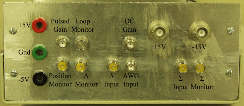
|
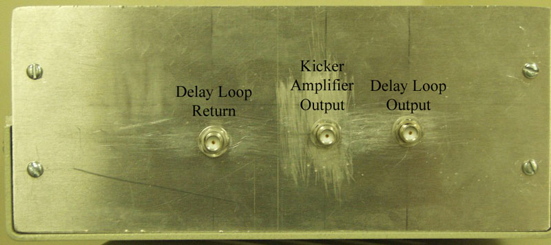
|
||||
| (a) Front panel | (b) Rear panel | ||||
|
|||||
All of the chips used in the feedback and normaliser circuit require a voltage supply of ±5 V. An external voltage supply of ±15 V is supplied to the board via 2 BNC cables. A Micrel Electronics MIC29300 low dropout regulator is used to drop the +15 V supply voltage to the required +5 V for the chip power supplies [116]; a National Semiconductor LM2990 negative low dropout voltage regulator is used to limit the negative supply at −5 V [117]. In order that the voltage supplies could cope with the demands of the rapid signal variation of the FONT BPM pulses, 10 µF capacitors were connected between ground and the input and output terminals of both voltage regulators. The purpose of these capacitors is to allow current to be drawn rapidly from the capacitors, before the power supply has had time to react, and keeping the power supply to each chip uninterrupted. For the same reason, a pair of 47 µF capacitors was connected between each power supply rail on the circuit board and ground, one at each end of the board. In addition, a 0.1 µF tantalum capacitor was connected between ground and both power supply pins of each chip, again to provide a rapid current source.
As mentioned previously, there is an inherent DC offset present on each of the signal pins of the AD835: in each case, a variable resistor network was used to cancel the effect of these voltage offsets. To facilitate accurate cancellation of these offsets, a systematic trimming procedure, proposed by Josef Frisch, was followed once the circuit had been fabricated: this trimming procedure is detailed in Appendix A.
The data acquisition system for FONT is similar to that already mentioned at the beginning of Section 4.7. Two Tektronix TDS684C 1 GHz four channel digitising oscilloscopes [118], each with a sampling rate of 5 Gs/s, provided the front end of the DAQ system, giving eight available DAQ channels. Four channels were required for the four monitor signals output from the feedback circuit: the raw BPM sum and difference, the normalised position and the feedback loop signals (see Figs. 5.24, 5.26 and 5.28(a)). As a corroborative measurement of the accuracy of the BPM sum signal, the output of Toroid 1750 was recorded; the voltage applied to the kicker magnet was also recorded using the same 100:1 pickoff arrangement as before (see Section 5.2.4). A seventh channel was used to measure the output of the signal generator used to produce the pulsed gain signal, to allow the timing to be measured and adjusted. Finally, the output of the AWG, used to produce the inverted charge signal, was recorded (see below).
The two oscilloscopes were set up outside the NLCTA tunnel: all the necessary cabling was run out of the tunnel through two ports in the roof, above quads QD1130 and QD1810 (see Figs. 5.1 and 5.2). This cabling consisted of six 3/8-in. heliax cables for each of the monitor signals and the AWG signal input, plus four BNC coaxial cables used to carry the two gain signals and the ±15 V power supply voltages. An Agilent E3630A DC power supply [119] was used to provide both the ±15 V supplies to the board and the DC gain voltage. A custom built rack mount splitter board, also situated outside the tunnel, was used to distribute the ±15 V from the power supply, with a variable resistor network used to supply and control the DC gain61.
Both scopes were connected via GPIB to a GPIB-to-TCP/IP network interface box: this allowed remote control of the scopes over TCP/IP using the GPIB protocol. A PC in the NLCTA control room was configured to be able to address the TCP/IP box over the existing NLCTA local area network. The PC was set up to control the scopes using the GPIB commands in Matlab: this allowed the complete integration of the FONT DAQ and data analysis, as well as easy data storage for offline analysis in the standard Matlab file format. A number of Matlab routines were written by Gavin Nesom to allow full GPIB control and DAQ of the scopes, providing a fully automated DAQ procedure. A number of subroutines were written to control the setup of the scopes (timebase, trigger, channel selection etc.) and the DAQ procedure, allowing easy adjustment of the various setup parameters. Also included was a subroutine to allow control of the AWG via GPIB (see below).
Both scopes were set up to use a common external trigger. This trigger pulse was provided by the NLCTA BPM micro TA02 responsible for acquiring data from the downstream end of the NLCTA62. As such, the scopes were set to acquire data at the same time as the NLCTA BPM's. This had the added advantage that the NLCTA BPM's had to be set up to acquire data whenever FONT was running so that the correct trigger signal could be provided for the scopes, meaning that it was a trivial process to collect data from the NLCTA BPM's with the SCP at the same time as FONT. The scopes were set up to acquire a single set of data: the Matlab routine would then retrieve that data from the scopes whenever they entered this “stopped” state. Once the DAQ process for a single data pulse had been completed, the scopes would be reset to the “single acquisition” state and the process would repeat. In this way, it was possible to ensure that the scopes would trigger only when the Matlab routine was ready to record the data.
Having acquired and recorded the data from a single pulse, the next stage is to calculate and output the inverted sum signal (1/Q) to the feedback circuit. An Agilent 33250A 80 MHz Arbitrary Waveform Generator (AWG) [120] was used to provide the inverted sum signal. An arbitrary waveform generator (or AFG: arbitrary function generator) is a signal generator that can be programmed to output any desired waveform, up to its bandwidth limit. The 33250A AWG is equipped with GPIB, to allow remote programming of the arbitrary waveform, and a dedicated trigger input. The trigger input allows the AWG to be programmed with the required waveform, which is then output whenever a trigger pulse is received. It is also possible to program in a delay time — up to 85 s and with 0.1 ns resolution — between the unit receiving the trigger pulse and outputting the desired waveform: this allows remote adjustment of the time at which the arbitrary waveform is output. This trigger delay, along with the AWG output mode and frequency, is programmed into the AWG as part of the initial setup subroutine of the DAQ program in Matlab. In truth, the bandwidth of the AWG arbitrary waveform output is limited not only by the 80 MHz bandwidth of the output, but also by the maximum sampling rate of the input waveform of 200 MHz, giving a maximum granularity of the inverted charge signal of 5 ns. However, it was felt that this provided sufficient bandwidth to produce an acceptable signal output [30].
Once the BPM data has been acquired and stored by Matlab, the inverted sum signal is calculated from the recorded BPM sum signal. A limit is placed on the magnitude of the inverted signal in software to prevent the AWG output going over 2 V: this keeps the signal input to the two first stage multiplier chips on the feedback board below the required 1 V signal maximum. If this limit was not put in place, the inverted signal would rapidly diverge to infinity as the sum signal drops away rapidly at the start and end of the pulse, overloading the signal inputs to the normaliser circuit. Once the inverted signal has been calculated, it is then sent via GPIB to the AWG. The AWG then outputs this waveform to the feedback circuit via a 3/8-in. heliax cable, as mentioned above, which carries the signal into the tunnel. The trigger for the AWG is provided by a separate crate on TA01, allowing the AWG waveform to be output prior to the beam reaching the FONT BPM. The exact timing of this trigger is then controlled using the trigger delay within the Matlab DAQ routine.
The final stage of the DAQ process is to save the recorded data to disk. The DAQ routine is set to run for a preprogrammed number of pulses: during each pulse, the data for that pulse is recorded in the Matlab workspace with a unique variable name. Once all the pulses have been recorded, the data for each pulse is recorded in a single .mat-file: this records the time and voltage information for each scope channel, plus the calculated inverted sum signal. The full DAQ program therefore encompasses the following subroutines:
As mentioned previously, at the end of Section 5.3.1, the reliable input voltage range for the AD835 multipliers used in the normaliser circuit is limited to 0.5 < Vin < 1 V. This limits the output of the sum and difference signals of the BPM processor to 0.1 < Vout < 0.2 V: this not only places a constraint on the peak output of the processor, but also on the flatness of the BPM signal i.e. the flatness of the charge distribution within the pulse. Independent of the absolute magnitude of either the sum or difference signals, it is a necessary condition that the charge distribution within the pulse not vary by more than a factor of 2 within the measurable portion of the pulse. This means that droops in the sum signal, such as those seen in Fig. 4.49, are unacceptable. Removal of these dips in the charge distribution was doubly important since such droops are thought to be the cause of the overshoot seen on the BPM difference signal (see Section 4.8.3 for details). It was therefore necessary to ensure that the beam was tuned to such a standard that such droops were not seen in the final FONT runs.
| Figure 5.29: Circuit diagrams of each of the stages in the FONT BPM signal pre-amplifiers [43]. Each pre-amp contains 3 of the 12 dB amplifier stages, plus one 6 dB and one 3 dB stage; the resistor networks ensure correct 50 Ω impedance matching for each stage. This also means that the gain of the amplifier is cut from ×8 to ×4. |
However, it was felt that, in order to limit the absolute magnitude of both the sum and difference signals to ±200 mV, a signal pre-amplifier should be used between the output of the BPM processor and the input to the normaliser circuit [121]. A pair of pre-amplifiers was designed and built by Colin Perry, based around the same AD8001 amplifier as used in the feedback circuit. Each pre-amp circuit provided an adjustable gain range between −9 dB and +36 dB in 3 dB steps. Each circuit consists of 3 gain stages and 2 attenuator stages: the circuit diagram of each of the stages is shown in Fig. 5.29. The attenuator section in each stage is remotely switchable via a series of relays, controlled from outside the tunnel via a custom-built multiple strand cable and selector switch. The cable also provides power for the six amplifiers in the circuit. Each amplifier is set always to be on: in this way, the signal delay through the entire pre-amplifier is independent of the gain selected. These pre-amplifiers therefore provided a method of remotely adjusting the voltage of the sum and difference signals output by the BPM processor.
In addition to the BPM pre-amplifiers, a remote method of adjusting the length of the delay loop was also discussed [121]. A delay box featuring a second relay assembly, with four relay stages, was designed and built by Colin Perry, making use of the same cable used to control the BPM pre-amps. This relay assembly follows a similar design to that of the 3 dB stage of the pre-amps shown in Fig. 5.29. However, the resistor network is replaced with a pair of external BNC connectors, allowing a BNC cable to be connected. The delay box is then placed in series with the delay cable, allowing the remote adjustment of the latency of the delay loop. The four external cables allow an additional delay of up to 42 ns to be added to the delay loop, allowing the latency of the delay loop to be remotely adjusted with a granularity of ~2.5 ns.
The FONT kicker amplifier is, from an electronics perspective, the most complex part of the entire FONT system. It was also the component that required the most intensive R&D to achieve the required signal output. A kick voltage of some 300 V is required for the kicker magnet to produce a modest position change of 1 normalised BPM Unit (see Section 5.2.3) — this corresponds to a power output of around 2 kW, for a rise time less than 5 ns. The equivalent requirement for the actual IPFB kicker driver is a maximum power output of 10 W (see Section 3.2.3). It was not possible therefore to use the design intended for use with the IPFB system for FONT, since the power requirements are so much greater [56].
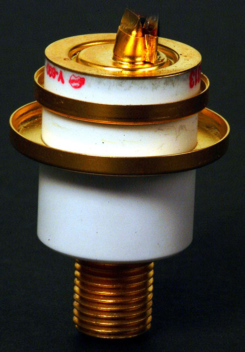
|
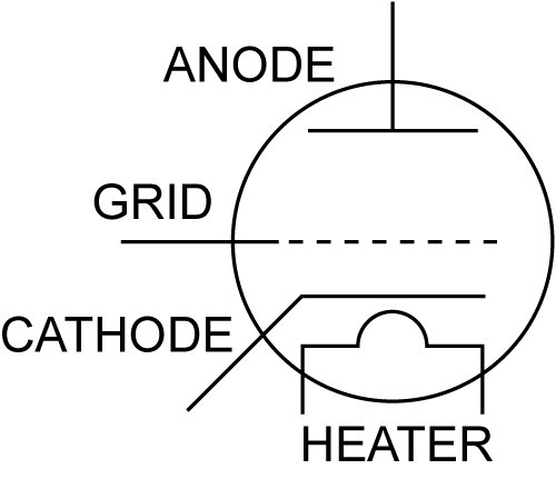
|
||||
| (a) Planar triode | (b) Triode tube diagram | ||||
|
|||||
As such, a new amplifier design had to be conceived in order to deliver the high power, low rise time requirements of the FONT system. Such an amplifier was designed and constructed by Colin Perry at Oxford University. This amplifier design is based around three Y690 planar triode tubes, which are used to amplify the incoming signal from the feedback circuit and power the signal that is used to drive the kicker magnet. The Y690 tube used for FONT is shown in Fig. 5.30, along with its circuit diagram. The planar triode is a particular type of tube designed for use at both high frequency and power [43]: it differs from a standard tube in that the internal connections — heater, cathode, grid and anode — are arranged parallel to one another in a planar arrangement, hence the name [123]. Otherwise, the planar triode operates in the same fashion as any other tube. A heater is used to heat a cathode and boil off electrons: these are accelerated towards an anode by a potential difference applied between cathode and anode. A modulating signal is applied to the grid, which controls the electron flow between cathode and anode: as such, the signal on the grid is amplified at the anode. The amplified signal is therefore picked off at the anode; the gain of the tube depends upon the applied bias voltage between cathode and anode.
The planar triode is normally used to amplify high frequency signals with a high output power. By decreasing the gap width between cathode, grid and anode, the electron drift time is reduced, increasing the bandwidth of the tube [122]: the Y690 can amplify signals up to 2 GHz [124]. However, it is not possible to make the planar triode too small, due to the large amount of heat generated during high power operation: this sets a limit on the size of the tube and therefore on the maximum output frequency [43].
| Figure 5.31: The electronics layout within the FONT kicker amplifier. The three planar triodes are encased within the black heat sinks in the centre of the box. The feedback signal and trigger inputs are on the right hand end of the box, with the high voltage supply input and kicker supply output on the left. |
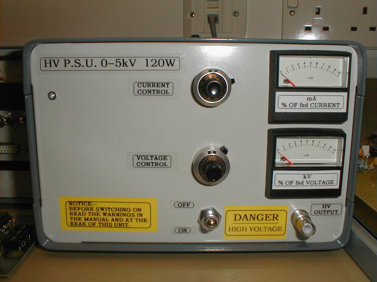
|
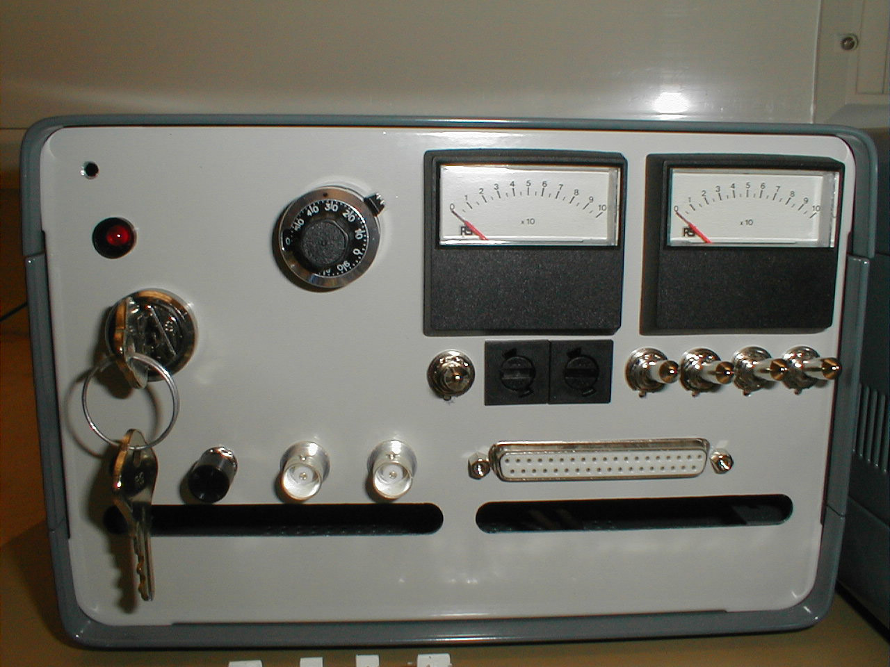
|
||||
| (a) PSU box | (b) Control box | ||||
|
|||||
As mentioned above, the Perry design for the FONT kicker amplifier makes use of three Y690 planar triodes to amplify the signal from the feedback circuit and drive the kicker magnet. The completed amplifier is shown in Fig. 5.31. The amplifier has a small pre-amp stage that amplifies the ±1 V output of the feedback circuit up to ±5 V. This ±5 V signal is then amplified again to the ±350 V signal used to drive the kicker magnet. The amplifier is designed to sit as close to the kicker as possible, and is connected to the kicker signal input with 1/2-in. heliax (see Section 5.2.3).
In addition, the amplifier has two external control boxes that sit outside the tunnel. The first provides the high voltage power supply that is used to power the tubes: this is brought into the tunnel on HV BNC cable. The second control box provides the trigger for the main amplifier. The amplifier operates by modulating the output pulse that is produced by the tubes when the bias voltage is first applied and the anode current begins to settle. Since the tubes must be powered on before the beam pulse arrives, this bias voltage must be applied in time for the beam pulse to arrive. As such, the amplifier uses a separate trigger to switch the tubes on around 3 µs before the arrival of the beam pulse. The trigger pulse is supplied to the amplifier from the control box via a 37-pin connector and cable that connects to the front of the control box. The two external control boxes are shown in Fig. 5.32.
Prior to installation of the FONT electronics inside the NLCTA tunnel, it was felt that a full system bench test would be vital in checking the correct operation of the system. As such, a tester circuit was designed by Josef Frisch and assembled by Tonee Smith at SLAC to provide simulated BPM difference and sum signals for the feedback circuit. The tester circuit was designed to recreate the sum and difference signals produced by the FONT BPM processor (see Section 4.6) and is described in Section 5.4.2. In order to do so, it was necessary to simulate the beam position and charge as seen by the BPM.
The simplest source of data for recreating the charge and position of the beam was the large quantity of previously collected BPM data. Using one of these many datasets would allow a large range of position and charge signals to be input to the feedback circuit, all from real measurements. A pair of Stanford Research Systems DS345 30 MHz Arbitrary Waveform Generators [125] was utilised to output these faked beam signals. The DS345 operates in the same fashion as the Agilent 33250A AWG used to produce the inverted sum signal. Each AWG can be programmed with an arbitrary waveform, with a specified frequency and magnitude, and output either at a predetermined time interval or in response to an external trigger signal. As such, it was possible to program one of the DS345's with a facsimile of the beam position and another with the beam charge.
As with the 33250A, the DS345 can be controlled through its GPIB interface. Although this gave the possibility that the DS345's could be programmed using the same Matlab GPIB routines used for the DAQ system, this could not be achieved in the short time available. As such, a series of LabView VI's used to control the DS345, written by Kirsten Hacker at SLAC, were modified for FONT's purposes by Tonee Smith and Stephen Molloy. These allowed each of the DS345's to be programmed with the specified charge and position waveforms. Each waveform could be selected from amongst a large set, allowing LabView to cycle through the set and provide a position and charge variation from pulse to pulse, rather than simply using the same pulse shape repeatedly.
LabView, however, requires data files in a different format than Matlab: tab-delimited .dat files as opposed to Matlab's proprietary .mat format. In order to provide LabView with the necessary waveforms, a selection of data from a previous run was converted to .dat format for use in LabView by Gavin Nesom. Since the BPM sum signal is an excellent measurement of the true beam charge (see Section 4.8.1), in each case the BPM sum signal was used to produce the beam charge waveform. For the beam position waveform, the normalised beam position was calculated using the recorded sum and difference signals, with the intention that the tester circuit should simply reverse this procedure (see Section 5.4.2). Both waveforms were then scaled to 1 V maximum amplitude.
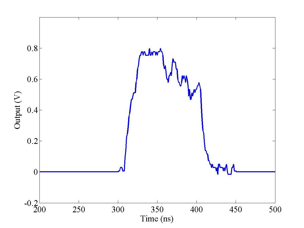
|
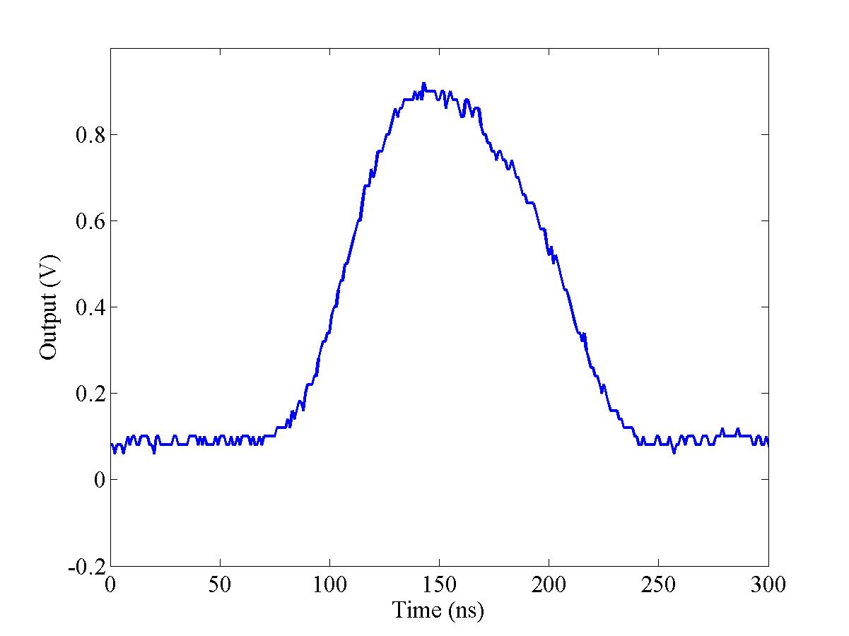
|
||||
|
|||||
However, having produced these simulated position and charge signals, it quickly became clear that the DS345 AWG's would be unable to reproduce these waveforms with the required granularity. The DS345 has an output bandwidth of 10 MHz for an arbitrary waveform, with a maximum sampling rate of 40 MHz: this corresponds to a minimum point spacing of 25 ns. As such, any features in the charge and position profiles shorter than around 50 ns in length would not appear on the simulated waveforms. The output of the DS345, using a real charge profile for the arbitrary waveform input, is shown in Fig. 5.33. This gave two possibilities:
Given that one of the main constraints on the real system was the limited beam pulse length of some 180 ns, it was felt that lengthening the simulated pulse would not gain anything for the simulation. Since neither case would be able to simulate the rapid charge variation seen on the real pulse (see Fig. 4.51), increasing the pulse length would only have further weakened the accuracy of the simulation. As such, it was also feasible to produce a number of position waveforms with flat or tilted profiles, without the detailed structure seen in the real beam, to provide some simpler cases for study. A selection of the simulated beam charge and position profiles is shown in Fig. 5.35 at the end of Section 5.4.3.
The purpose of producing simulated position and charge signals, as opposed to sum and difference signals, is that, although the feedback circuit requires the BPM sum and difference signals as its inputs, the corrective output signal is given in terms of the beam position i.e. a voltage to be amplified and applied to the kicker magnet, which causes a change only in the beam position. Since one is attempting to feed the output of the feedback circuit back to the input to replicate the effect of the kick applied to the beam, it is simpler to do this in terms of the beam position (multiplying position and charge to produce the difference signal) than the BPM difference signal (dividing difference by sum to give beam position). As mentioned previously, a tester circuit was fabricated to simulate the signal output of the beam components that are not present for the bench test i.e. the BPM sum and difference signals produced in response to the FONT system correction.
| Figure 5.34: Circuit diagram of the FONT feedback tester circuit. The charge signal passes through the splitter and is output as the sum signal; the multiplier chip uses the position and charge signals to produce the difference signal. The corrective output from the feedback circuit is summed at the position input. |
A circuit diagram of the tester circuit is shown in Fig. 5.34. The circuit is constructed around the same AD835 multiplier chip used for the feedback circuit. The power supply for this tester circuit was provided by the ±5 V connections on the front of the feedback box. The tester circuit takes the two simulated position and charge signals produced by the DS345 AWG's as its inputs. The charge signal is first split using a resistive splitter network: half the signal goes straight to the sum input of the feedback circuit to simulate the sum signal. The other half is used by the tester circuit to produce the simulated difference output. The charge signal is input to the X1 input of the AD835; the X2 input is used to correct the mutual voltage offset of the two inputs in the same manner as the other AD835's used in the feedback circuit (see Section 5.3.1 and Fig. 5.25 for details of the pin arrangements of the AD835 chip). The Z input also serves the same purpose, acting as an offset adjust for the voltage offset of the Z input and W output63.
The simulated position signal is input at Y1: with this setup, the signal seen at the output of the chip would therefore be the product of position and charge, which is, to a good approximation, the BPM difference signal. However, this setup would not include the corrective effect of the feedback circuit. Therefore, the output of the feedback circuit that would normally go on to the kicker amplifier is input to the Y2 input of the AD835. Since the kicker amplifier should have a linear input-output response, the amount that the beam is kicked by the kicker — and therefore deflected at the BPM — has a linear dependence on the output of the feedback circuit. As such, it is perfectly acceptable for the purposes of the simulation to have the output of the feedback circuit directly affect the simulated beam position. It is then possible to vary the magnitude and direction of this change in beam position by varying the sign and magnitude of the DC gain input to the feedback circuit.
In this way, the tester circuit simulates the effect of the feedback circuit correcting the position of a misaligned beam. The output of the feedback circuit is connected to the feedback loop input of the tester circuit via a 32 ns long BNC cable, to simulate the round trip time of the real FONT system. Initially, the same trigger signals as described in Section 5.3.3 were used for the FONT 33250A AWG and the scopes, to allow the feedback circuit to operate as closely as possible to the real beam test. In order to synchronise the test AWG's to the feedback circuit and AWG, the trigger output of the 33250A was used to trigger the two test AWG's.
A problem occurred with the initial setup of the triggers, since the test AWG's could only be synchronised to their 10 MHz clocks: although they would receive the trigger input from the 33250A at the correct time, the output would be delayed until the next clock cycle. This meant that the output of the test AWG's would not arrive at the same time for consecutive pulses within the acquisition window of the scopes. As such, the inverted signal produced by the 33250A would no longer align correctly with the simulated sum and difference signals due to the timing jitter. The eventual solution was to lengthen the output pulse of the position AWG to 500 ns, arriving before the start of the charge pulse. The FONT AWG and oscilloscopes were then set to trigger on the trigger output of the charge AWG, allowing all the components to be synchronised on each pulse.
Before the feedback circuit was tested with the simulated beam pulses, a series of measurements was made on the signal propagation delay of each component in the feedback circuit. A 500 ns 500 mV square pulse was input to the sum, difference and AWG inputs of the normaliser circuit: the sum and difference inputs each had a 14 dB attenuator connected in series to drop the input voltage to 100 mV. The signal path between the pulse generator and the AWG input was the shortest, allowing measurements to be made on the leading edge of the sum and difference pulses. With a ~700 mV DC signal input to the DC gain, the output of the circuit was measured to be ~400 mV, with a pulse length roughly the same as the input pulses.
| ||||||||||||||||||||||||||||||||||||||||||||||||||||
| ||||||||||||||||||||||||||||||||||||||||||||||||||||
The signal delay through each component was measured by using a scope probe at the input and output pins of each chip in the signal path. The half height voltage of the square pulse was used to measure the time difference between the reference point — the input of the difference pre-amp — and the measurement point. The signal delays for each component are summarised in Table 5.2. It is interesting to note that, although the signal delay through each of the AD835's is constant at around 1.7 ns, the delay through the AD8001's appears to be gain dependent, since the ×5 amplifier is almost half a nanosecond faster than the two ×10 amplifiers. This is consistent with the gain dependent bandwidth specifications of the chip [115]. The full circuit delay was measured to be 10.5 ns between the external SMA connectors of the difference input and the feedback output.
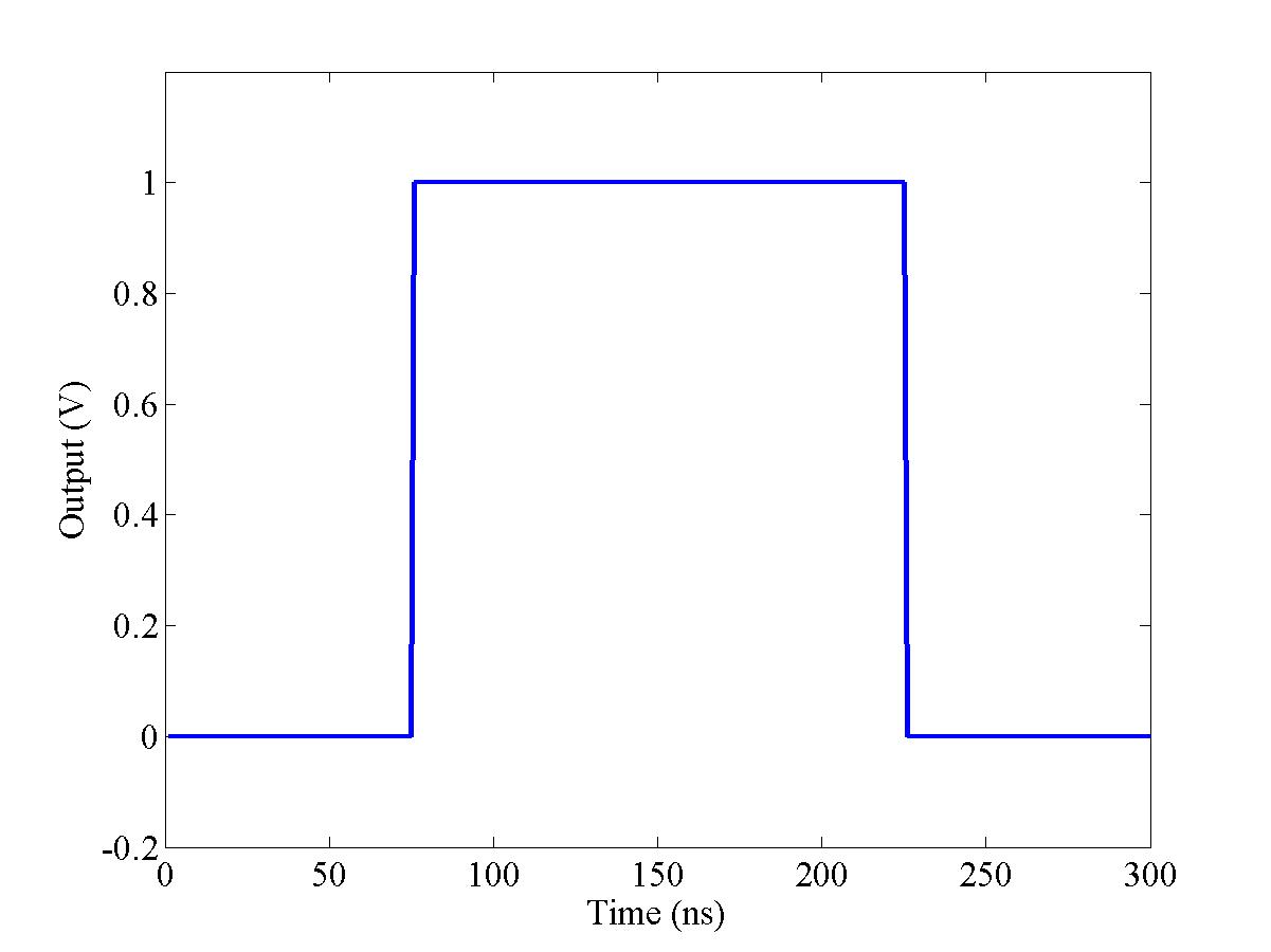
|
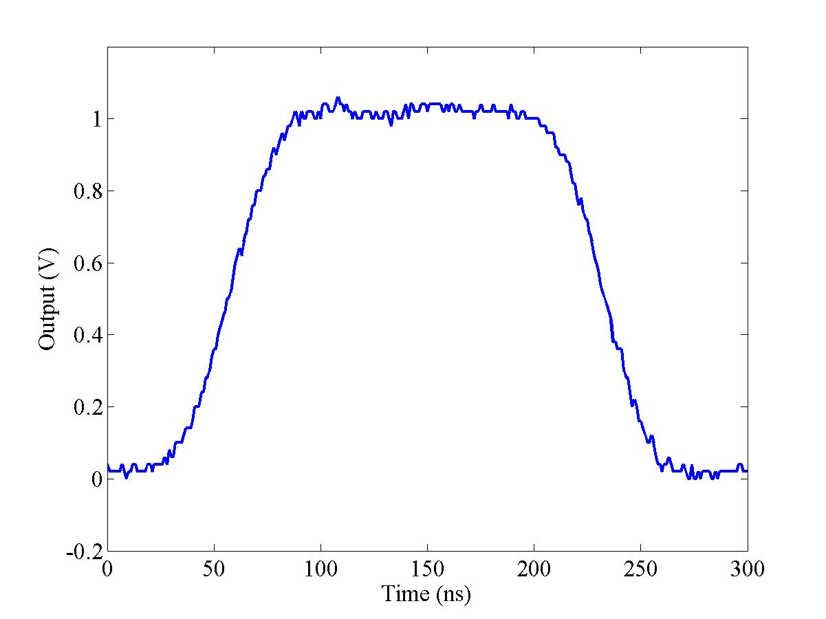
|
||||
| (a) Flat charge distribution | |||||
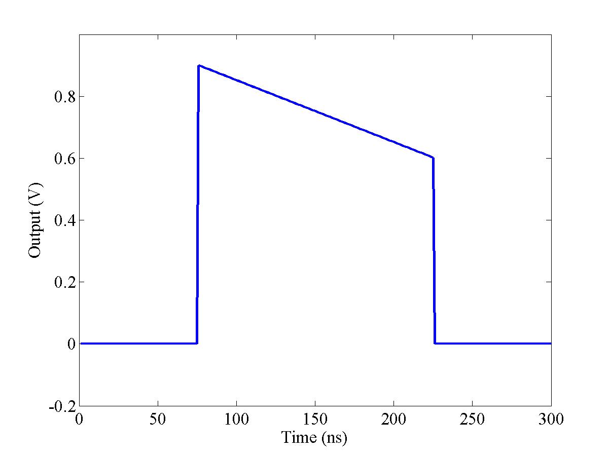 |
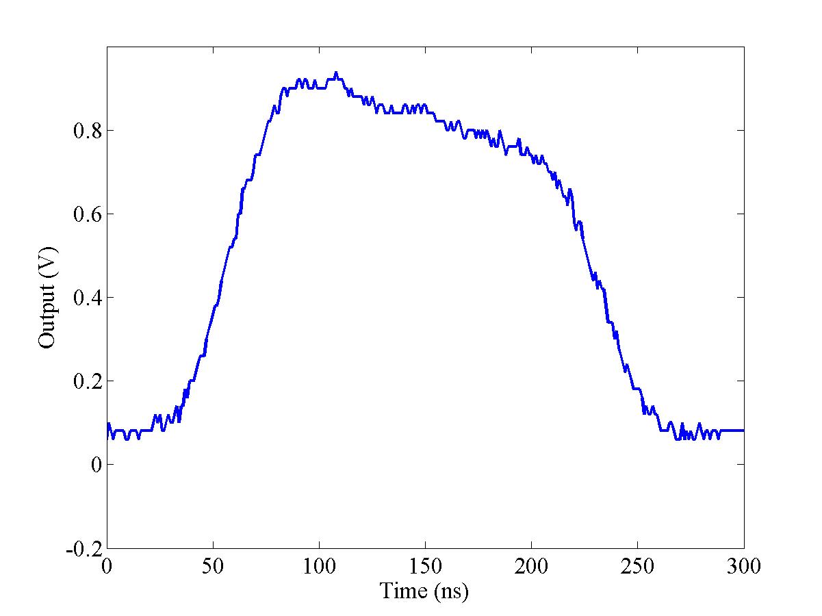 |
||||
| (b) Tilted charge distribution | |||||
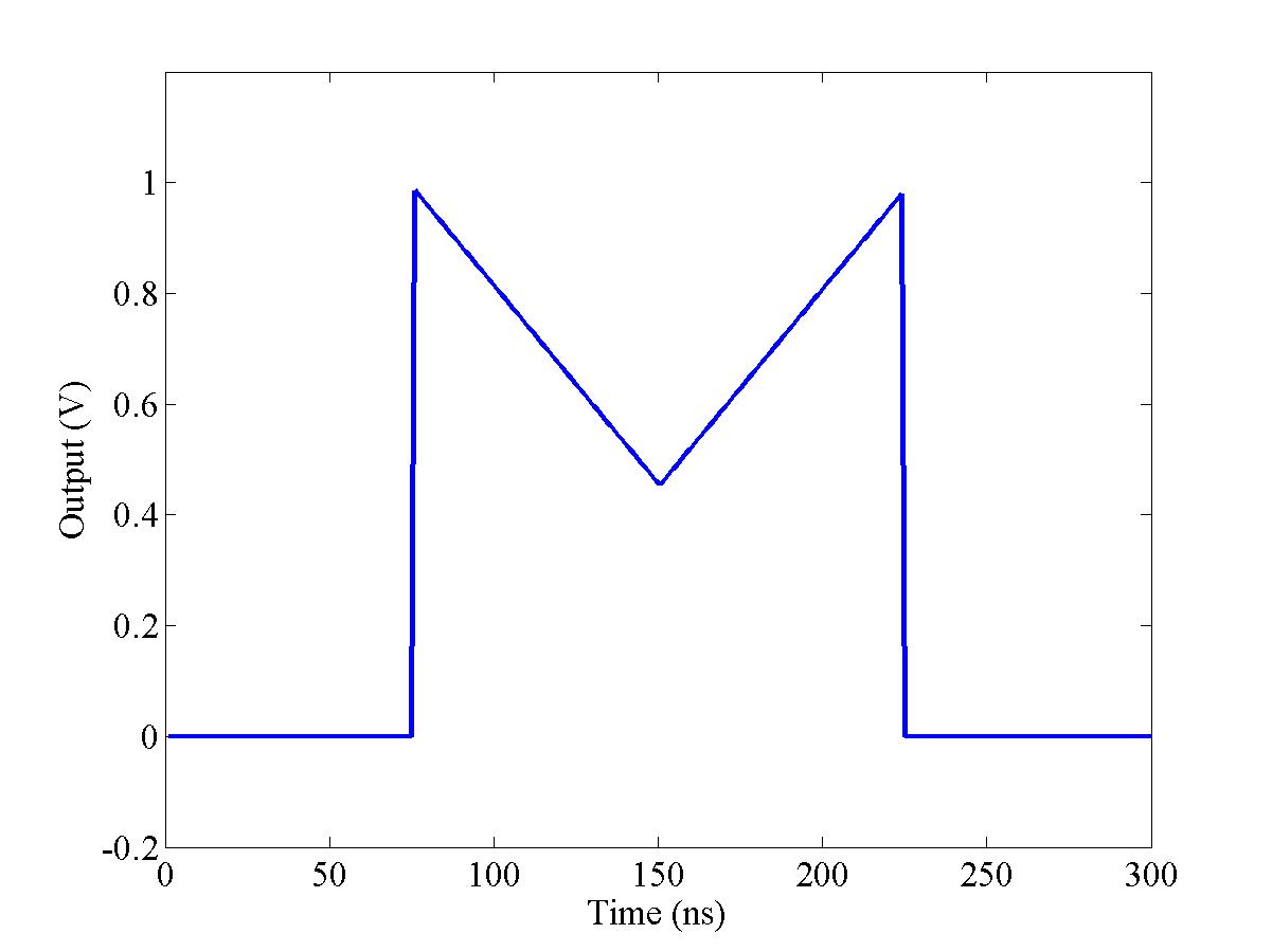 |
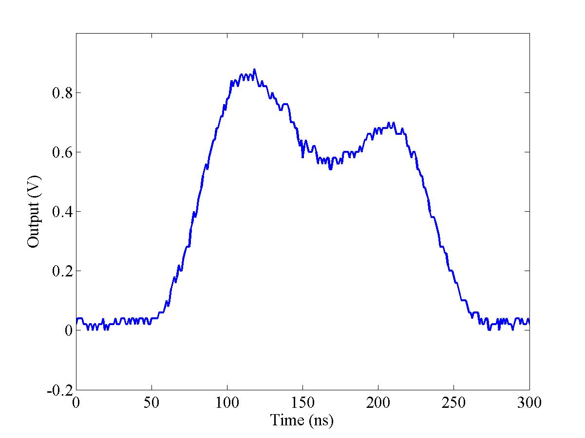 |
||||
| (c) Realistic charge signal | |||||
|
|||||
The full bench test of the feedback circuit was carried out in two parts: firstly without, and then with the delay loop. In both cases, the types of input pulse used were the same: the charge input signals are shown in Fig. 5.35. It is clear to see the effect of the bandwidth limit applied by the DS345 AWG: each of the pulses shown in Fig. 5.35 shows a significant smoothing between the input and output waveform of the DS345 (this is the reason for the shape difference of the two pulses shown in Fig. 5.35(c)). It is for this reason that these manually created charged distributions were used for a number of the tests. Since the complex charge variation seen on the real beam charge distribution is not repeated with the AWG pulse (see Fig. 5.33), the fake charge distributions allow a greater degree of manipulation of the signals input to the feedback circuit.
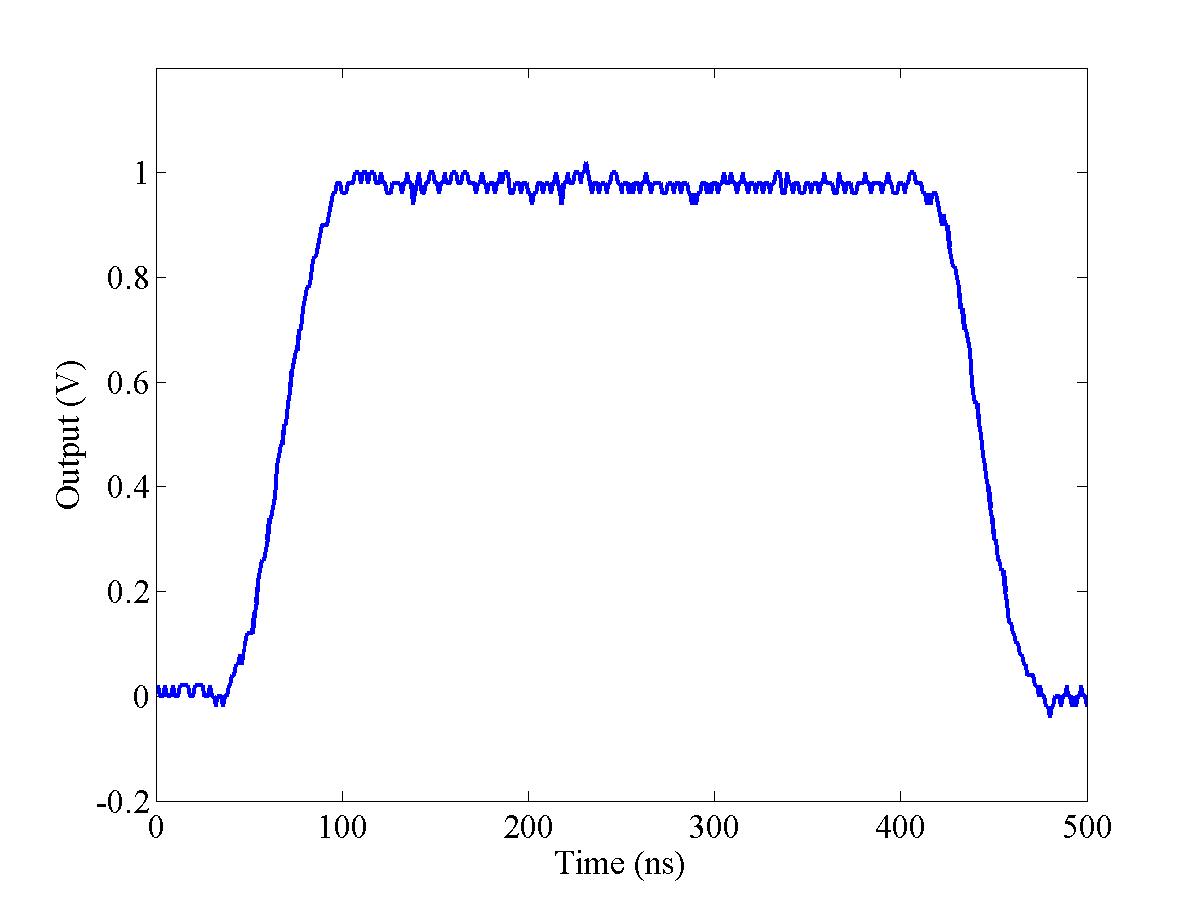
|
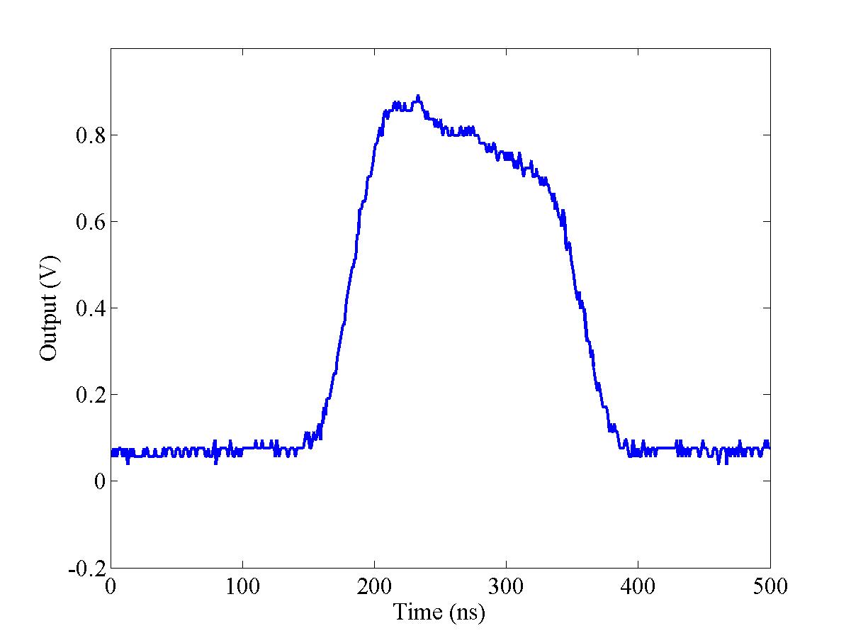
|
||||
| (a) Position signal | (b) Difference signal | ||||
|
|||||
The corresponding position signal is shown in Fig. 5.36(a): note that, as mentioned above, the position signal is considerably longer than the various charge signals shown in Fig. 5.35. The position signal was timed to arrive at the tester circuit some 100 ns before the charge signal. Using the charge profile shown in Fig. 5.35(b), the resultant difference signal output of the tester circuit (without the feedback circuit) is shown in Fig. 5.36(b). Since the position signal is essentially a 450 ns square pulse, the difference signal carries the shape of the charge signal, in a similar manner to the true sum and difference signals shown in Fig. 4.53.
| Figure 5.37: The output of the feedback circuit for the simulated beam charge profile shown in Fig. 5.35(a). The signals shown are: simulated sum signal (blue), simulated difference signal (black), FONT AWG 1/Q output (green) and feedback circuit normalised output (red). |
The resulting output of the feedback circuit, without the use of the delay loop, is shown in Fig. 5.37. The sum signal measured by the feedback circuit (blue) follows the expected profile. The FONT AWG signal (green) is clearly an inversion of the sum signal. The rapid cutoff that occurs at either end of this signal is a result of the limit that prevents the AWG signal from going over 2 V, as mentioned in Section 5.3.3. The AWG pulse sets the maximum length of the beam pulse that the feedback circuit processes: in this case, this is 180 ns.
The difference signal (black) exhibits the behaviour that one would expect from the circuit without the delay loop in operation. Initially, it follows the contour of the sum signal. At 100 ns, the effect of the offset has been measured by the feedback circuit, and a correction attempted. At this point, the simulated beam is steered down, towards the BPM ‘centre’, and the simulated difference signal drops accordingly. After another latency period, at 145 ns, the corrected beam has been registered by the feedback circuit: since the delay loop is not connected, the system has no memory of its previous correction and the difference signal (and beam position) returns to its previous level, essentially setting the system back to its initial state. After a further latency period, at 190 ns, the feedback circuit has once again measured the simulated beam offset and applied a correction to the beam position, which is reflected in the difference signal. Finally, at around 230 ns, the AWG 1/Q pulse switches off, preventing the feedback circuit from applying any further correction: the difference signal then returns to follow the sum signal as it drops back to zero.
The normalised output of the feedback circuit is shown on Fig. 5.37 in red. In some sense, this is the most important indicator of the health of the feedback circuit, since it is an indicator of where the feedback circuit thinks the beam is. The primary feature of the normalised signal is that it has roughly the same shape as the difference signal. More importantly, however, the normalised signal a) is clearly gated by the AWG pulse, since it rises sharply at 65 ns, and b) does not share the pulse shape of the sum signal at its leading or trailing edges. This can be seen clearly on the leading edge of the normalised signal: instead of showing the slow rise of the difference signal, the normalised signal has a sharp edge and plateau, indicating that the beam position is flat. It is possible to see the 11 ns latency of the feedback circuit: this is the cause of the delay between the black and red traces.
Also clear from the normalised signal is the cumulative effect of the bandwidth limit of each of the components of the feedback circuit. Although the normalised output shows a sharp leading edge, the rising and falling edges of the pulse become consistently slower with consecutive latency periods. This is likely to be caused by the limited bandwidth of the normaliser and feedback stages of the circuit, and results in a continuous smoothing with each successive pass round the feedback loop. This smoothing is likely to be exaggerated slightly by the AD835 used as part of the tester circuit and the 32 ns-long coaxial cable connected between the output of the feedback circuit and the feedback input of the tester circuit.
| Figure 5.38: The output of the feedback circuit for the simulated beam charge profile shown in Fig. 5.35(b). The signals shown are the same as those of Fig. 5.37. |
| Figure 5.39: The output of the feedback circuit for the simulated beam charge profile similar to that shown in Fig. 5.35(c). The signals shown are the same for those of Fig. 5.37. |
| Figure 5.40: The output of the feedback circuit for the simulated beam charge profile similar to that shown in Fig. 5.35(c) but with the addition of the delay loop. The signals shown are the same for those of Fig. 5.37. |
Both the initial normalised signal flatness and the signal smoothing can be seen on the normalised signal in Figs. 5.38 and 5.39: these show the same data as Fig. 5.37, but with two different charge profiles. Both the normalised position and the difference signals show the same general shape as seen in Fig. 5.37, but the effect of the altered charge profile can be seen on the difference signal and AWG output. The relative height of the peaks in the normalised signal is also similar between each of the three charge profiles. However, the dip in the signal after ~120 ns and the second peak at ~180 ns both show a small spike on the trailing edge. It is interesting to note that similar features also appear in the original IPFB simulations shown in Fig. 3.21. It was not possible, in the short time available, to fully establish the cause of these spikes. It is likely, however, that the feedback circuit is operating as designed, since the deviations between the normalised signals of Figs. 5.37-5.39 are small.
The next stage in the bench test was to include the feedback loop. The variable delay loop control, described in Section 5.3.4, was also included, to allow accurate adjustment of the length of the delay loop. Using the charge profile shown in Fig. 5.35(c), the output of the feedback circuit is shown in Fig. 5.40. Again, the sum signal (blue) shows the double peaked shape seen previously, with the AWG 1/Q signal (green) clearly the inversion of this signal, with a cutoff at around 2 V. However, when compared with Fig. 5.39, the difference and normalised position signals now clearly show the effect of the delay loop. After the second latency period, instead of rising back to the original level, both signals now continue to step towards zero, indicating that the simulated beam is being slowly steered back towards the centre of the BPM.
| Figure 5.41: The normalised output (red) and delay loop signal (black) for the feedback circuit using the simulated pulses shown in Fig. 5.40. The point at which the delay loop acts for each latency period is shown on the plot (marked ‘1’, ‘2’ and ‘3’); each trace is the average of 10 measurements. |
The normalised position signal is shown separately in Fig. 5.41. It is clear that the beam position exhibits the stepping behaviour characteristic of the IPFB design described in Section 3.2. The simulated beam position shown in Fig. 5.41 compares extremely favourably with the original IPFB simulations, such as those shown in Fig. 3.20. Even with the noise inherent in the FONT electronics, there is a clear similarity between the beam positions shown in Figs. 5.41 and 3.20(b).
Also shown in Fig. 5.41 is the signal that passes into the delay loop: here the intended iterative behaviour can be seen. The first two corrective stages are clear, with a third just visible: these are marked on the figure. Beyond this, there is no longer any source signal, since the simulated input signals are no longer present, and the feedback signal continues to run around the delay loop until it decays back to zero. It is therefore possible to conclude from these simulations that, within the scope of the bench test, the FONT electronics perform as intended.
Having completed the bench testing of the FONT feedback electronics, the final stage was to test the full FONT system on the beam line at the NLCTA. A number of different tests were carried out to test the correct operation of the full system. These are described in the remainder of this chapter.
| ||||||||||||||||||||||||||||||||||||||||||
|
With the FONT BPM processor installed directly below the BPM (see Fig. 4.29), and the X-band amplifier situated around 50 cm upstream, this left around 3 m of available space to install the complete FONT system. The intention was to decrease the latency of the system by minimising the amount of cable used to connect components, ideally to be little more than the ~4 m between the front end of the kicker and the BPM. Latency measurements of the various components in the FONT setup are shown in Table 5.364 (see Fig. 5.3 for detail of the beam components in the FONT area). The total system latency of 67.0 ns is almost double that of the expected IPFB latency (see footnote 19): however, since the beam flight distances are similar to that suggested for the IPFB, this extra delay is due to the extra processing time required to deal with the high power signals involved and the associated signal delays from using cables with a speed less than c.
| Figure 5.42: The arrangement of the pre-amp and feedback circuits and associated cabling for the final FONT installation. The control connections for the pre-amp gain can be seen at the top of the silver pre-amp box. |
| Figure 5.43: The output connections of the feedback circuit and the delay loop. The variable delay box is controlled via the grey ribbon cable, connected to the left side of the box with the blue connector. |
In order to achieve this expected system latency, it was necessary to install each of the FONT system components directly below the beam line. The 0.5 m of excess cable length mentioned in Table 5.3 takes into account this arrangement, making the assumption that, although the girders on which the FONT system would be placed are only ~0.3 m below the beampipe, there is always some additional cable length taken up in connecting components. The variable pre-amp box was placed upstream of the BPM processor, between quads QD1650 and QD1760, with the sum and difference inputs of the pre-amp connected to the output of the BPM processor mixers with a pair of 80 cm coaxial SMA cables. The pre-amp box was then connected to the feedback circuit with a pair of 5 cm coaxial SMA cables. The ±15 V power supply for the feedback circuit was brought in on a pair of BNC cables; the gain signals were also brought in on BNC cables, with the AWG input and the four monitor output signals carried on 3/8-in. heliax. The pre-amp and feedback circuit assembly in the NLCTA tunnel is shown in Fig. 5.42. The delay loop and variable delay box were placed just upstream of the feedback box: this is shown in Fig. 5.43.
| Figure 5.44: The FONT kicker driver installed in the NLCTA next to the kicker magnet. The kicker amplifier input is on the right of the box: the large grey cable carries the control and trigger signals. |
| Figure 5.45: The fully installed FONT system, enclosed within its lead shielding below the NLCTA beampipe. The quad in the centre of the picture is QD1650. |
The kicker amplifier was placed on a different girder, between quads QD1550 and QD1650, with its input connected to the output of the feedback circuit with a 3/8-in. heliax cable; the installed kicker amplifier is shown in Fig. 5.44. The kicker amplifier was then connected to one of the upper input connectors of the kicker magnet with a 1 m length of high voltage heliax cable. The output of the kicker magnet remained connected to the high voltage 50 Ω terminator described in Section 5.2.4, to allow measurement of the kicker pulse outside the tunnel. Finally, once all the equipment had been installed, it was encased in lead shielding to protect the more sensitive parts of the electronics from radiation damage during accelerator operation. The completed installation can be seen in Fig. 5.45.
Before carrying out a complete test of the FONT system, it was necessary to check the performance of the normaliser stage of the feedback circuit. Since the linear behaviour of the FONT magnet assembly (Section 5.2) and the linear response of the X-band BPM (Section 4.8.2) had already been measured, it was expected that the normaliser circuit would also show the same linear behaviour.
To test the response of the feedback circuit, the SCP was set up to steer the beam with the FONT dipole and YCOR 1650, in the same way as described in Sections 4.8.2 and 5.2.2. The two dipoles were first adjusted until the beam appeared to be travelling as close to the centres of QD1650 and QD1760, as measured by NLCTA stripline BPM's 1651 and 1761. The FONT dipole was then steered through 10 positions, in steps of 21 × 10−2 G-m, with 5 beam pulses recorded at each position. The FONT dipole was then re-centred and YCOR 1650 steered through 13 positions, in steps of 50 × 10−2 G-m, with 5 beam pulses recorded at each position.
| Figure 5.46: The normalised signal output from the normaliser stage of the FONT feedback circuit for 10 settings of the FONT dipole. Each trace is the average of 5 pulses. |
| Figure 5.47: The normalised BPM position signal for 10 settings of the FONT dipole. The normalised position is calculated from Δ/Σ as before; each trace is the average of 5 pulses. The noise at the start and end of each pulse is the result of dividing two very small signals. |
The normalised signal output of the feedback circuit in response to the variation of the FONT dipole is shown in Fig. 5.46. The same stepping is evident as that shown previously in Fig. 4.55 in Section 4.8.2 as a result of the variation in field strength of the FONT dipole. This figure should be compared to Fig. 5.47: this shows the same information, but the normalised position is calculated, as before, using the raw BPM sum and difference signals. In theory, if the feedback circuit worked perfectly and had infinite bandwidth, these two figures should be identical. However, this is not the case: there is clearly more ‘noise’ on the calculated signal in Fig. 5.47 than on the signal in Fig. 5.46. It is also interesting to note that the noise along the length of each individual beam pulse becomes larger the further the beam is steered from the centre of the beampipe. This could be a result of the beam scraping on the BPM aperture and degrading the beam quality, or some nonlinearity in the response of the BPM. It was not possible at the time to determine the cause of this effect.
| Figure 5.48: A comparison of the normalised signal output of the feedback circuit, shown in red, with the calculated normalised position, shown in black. The normalised position is calculated from Δ/Σ as before; 5 positions are shown with 5 beam pulses at each position. |
A comparison between the two normalised signals is shown in Fig. 5.48. The normalised signal output of the feedback circuit is shown overlaid with the calculated position signal. Two features are clear from this figure: firstly, the two methods used give very similar position measurements, both showing the clear stepping resulting from the variation of the dipole; secondly, the circuit output is noticeably smoother than the calculated position. The likely explanation for this smoothing is that, while the only bandwidth limit on the calculated signal is the sampling rate and bandwidth of the oscilloscopes used in the DAQ system, the feedback circuit is also bandwidth limited by its internal components. While the scope has a 1 GHz bandwidth, the feedback circuit is bandwidth limited by 4 AD835's (250 MHz bandwidth [114]) and 3 AD8001's (260 MHz bandwidth at ×10 gain [115]), as well as the 80 MHz bandwidth of the AWG used for the 1/Q signal. It is highly likely that this is also the reason for the signal smoothing seen in the bench tests (Section 5.4.4).
| Figure 5.49: The mean normalised signal output of the feedback circuit as a function of the integrated field of the FONT dipole for all 50 beam pulses. The mean signal is calculated from the average of the feedback circuit normalised signal output over the central 100 ns of the pulse. The red line is a line of best fit produced through a χ2 minimisation. |
However, given these limits inherent in the feedback circuit electronics, there is still a good deal of agreement between the calculated and the circuit position responses. The normalised position response of the circuit as a function of the FONT dipole field strength is shown in Fig. 5.49. The same linear response as observed in Section 5.2.2 is evident, and the BPM sensitivity of 0.891 ± 0.007 BPM Units per G-m of FONT dipole field strength compares favourably to the previously measured value of 0.835 ± 0.011 BPM Units per G-m (extracted from Fig. 5.11). It is also possible to see, in Fig. 5.48, the point at which the AWG signal switches on and off: there is a clear ramp up at 110 ns and a similar ramp down at 270 ns. This sets the usable pulse length at ~160 ns.
| Figure 5.50: The mean normalised signal output of the feedback circuit as a function of the integrated field of YCOR 1650 for 65 beam pulses. The mean signal is calculated as before. The red line is a line of best fit produced through a χ2 minimisation. |
The corresponding plot to Fig. 5.49 for YCOR 1650 is shown in Fig. 5.50. Again, a very clean linear response is observed from the normalised position produced by the feedback circuit, and compares well with the previous dataset shown in Fig. 4.58. As with the FONT dipole, the BPM sensitivity of 0.365 ± 0.009 BPM Units per G-m of integrated field strength for YCOR 1650 is an acceptable match to the measurement given in Section 4.8.2 of 0.323 ± 0.010 BPM Units per G-m. This dataset also gives a minimum r.m.s. deviation in normalised beam position of 0.004 BPM Units for each dipole setting, for both the calculated and measured normalised positions. This is an improvement over the jitter measured in Section 4.8.2 of 0.007 BPM Units, and corresponds to a jitter of just 12 microns. However, this figure is likely to be less sound since it is obtained from a dataset less than half the size of the previous one.
It is therefore a straightforward conclusion that the normaliser stage produces an accurate measure of beam position given the sum and difference signals produced by the BPM processor.
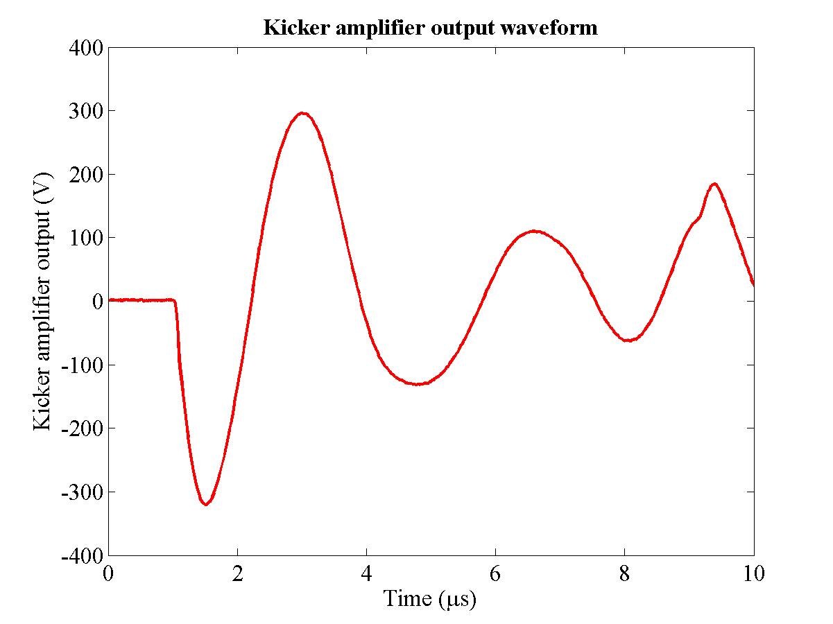
|
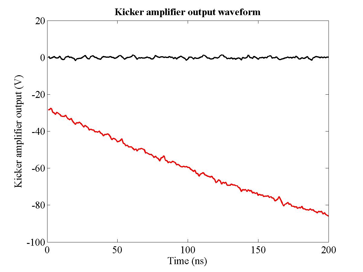
|
||||
| (a) Kicker amplifier output | (b) Close-up of modulated region | ||||
|
|||||
Having tested the normaliser stage of the circuit, the first stage in testing the full FONT system is to the measure the performance of the kicker amplifier. As mentioned in Section 5.3.5, a trigger signal is used to switch on the tubes within the kicker amplifier some 3 µs before the arrival of the beam. This pulse is then modulated with the signal produced by the feedback circuit to drive the kicker magnet and steer the beam. The output pulse of the kicker amplifier is shown in Fig. 5.51(a). This is the raw output of the kicker amplifier without any input from the feedback circuit. A close-up of the region on which the feedback circuit output is superimposed is shown in Fig. 5.51(b).
It is necessary to operate the amplifier in this fashion in order to produce the 2.5 kW power output required to drive the kicker magnet. However, since the nominal amplifier output shown in Fig. 5.51(b) (red trace) is not flat, not only will the whole bunch train experience a net downwards kick due to the overall offset, but the back of the bunch train will receive a larger kick than the front, due to the slope. While a net offset will not affect the overall operation of the feedback system65, it is vital that the slope on the kicker pulse is small compared to the beam offset at the FONT BPM.
| Figure 5.52: The normalised beam position with the kicker amplifier on (blue) and off (black), but receiving no input from the feedback circuit. Note that there is a discernable difference between the two traces as a result of the unmodulated kicker amplifier output. Each trace is the average of 30 beam pulses. |
| Figure 5.53: The difference between the two traces shown in Fig. 5.52. The approximate slope on this difference plot is overlaid in red, with the start and finish of the pulse marked in black. |
The effect of this slope on the beam position is shown in Fig. 5.52. 30 beam pulses were recorded with the kicker amplifier on, but receiving no input from the feedback circuit, and 30 pulses with the kicker amplifier off, with the beam steered upwards by the FONT dipole. There is a clear difference between the normalised beam positions for both cases. By taking the difference between these two pulses, it is possible to analyse the effect of the unmodulated kicker amplifier output on the beam position: this is shown in Fig. 5.53. Although a large peak appears in the middle of this difference plot, it is likely that this peak as a result of the degradation of the beam quality between the two sets of measurements. However, there is also a general trend, marked with a red line, indicating that there is a slope on the beam position as a result of the unmodulated kicker amplifier output. However, the difference between the amplitude of the start and end of this pulse is only 40 mV, while the maximum normalised position seen in Fig. 5.52 is around 800 mV. It is unlikely that an effect on the 5% level such as this will have any adverse effect on the performance of the FONT system.
Finally, the full range of the kicker driver was measured. The kicker amplifier output voltage was measured to saturate at +250 V and −350 V, with an offset of −50 V due to the amplifier output waveform shown in Fig. 5.51(a). This sets the maximum voltage swing at ±300 V: this corresponds to a range of 42 × 10−2 G-m for the FONT dipole. As such, the gain settings of the feedback pre-amp box were set such that the difference signal input to the normaliser stage was between ±1 V for this range for all the data recorded with the feedback system.
| Figure 5.54: The normalised beam position signal for 5 different settings of the FONT dipole. Each trace is the average of 10 beam pulses. |
The next stage was to measure the performance of the FONT system without the delay loop. The results should mirror those of the bench tests presented at the start of Section 5.4.4. By switching on the DC gain signal of the feedback circuit and allowing the feedback circuit to drive the kicker amplifier, it is possible to apply a single loop correction to the measured beam offset. With the delay loop switched off, the beam was steered through five different positions with the FONT dipole, in steps of 8.4 × 10⁻² G-m, with 10 beam pulses recorded at each position. The normalised beam position with the kicker amplifier off is shown in Fig. 5.54. Note that, although there is the same stepping in normalised position as a result of the beam being steered by the FONT dipole, the variation in position along the length of the bunch train is of the same order of magnitude as this stepping. However, this bunch train shape is repeatable: the r.m.s. pulse-to-pulse jitter was observed to be around 10% of the position variation along the length of the train. This means that, although the shape of the bunch train is far from ideal, it is still possible to operate the feedback system, since the kicker is quite capable of moving the beam over a larger range than that of the pulse-to-pulse jitter.
| Figure 5.55: The normalised beam position signal with the feedback circuit on, running at low gain, with the delay loop off. The black lines mark the start and end of the feedback circuit correction. Each trace is the average of 10 beam pulses. |
| Figure 5.56: The normalised beam position signal with the feedback circuit on, running at high gain, with the delay loop off. The black lines mark the start and end of the feedback circuit correction. Each trace is the average of 10 beam pulses. |
The same set of measurements was then repeated using the feedback circuit to attempt a single loop correction of the beam position offset. Two different gain settings — a “low gain” setting of 0.5 V and a “high gain” setting of 1 V — were used for the feedback circuit DC gain, to measure the effect of the circuit gain on the position correction. The low gain response is shown in Fig. 5.55, with the high gain case shown in Fig. 5.56. The effect of the feedback circuit correction can be seen in both cases. For the low gain setting, the beam is steered towards the centre for each of the 5 beam positions. Since the delay loop is not in use, after a single latency period the feedback circuit tries to make a correction based on the corrected part of the bunch train, and the beam is no longer steered as strongly by the kicker magnet.
A similar effect is observed with the high gain setting. In this case, the gain is set closer to the ‘ideal’ setting and, for each of the 5 beam positions, the beam is steered back to the centre of the BPM after a single latency period. Again, after another latency period the feedback circuit stops seeing an offset, and the beam returns to its original position. Even though the beam position for a single pulse shows a great deal of variation along its length, Fig. 5.56 shows a response that is similar to the bench test results shown in Fig. 5.37. Since the feedback system is unable to correct the fine scale position variation, this is exactly the response that one would expect from the feedback system.
It is also possible, using these results, to measure the latency of the full feedback system and use this to set the length of the delay loop for the full system operation (see Section 5.5.5). Using the data shown in Fig. 5.56, the latency is the delay between the start of the pulse and the point at which the feedback correction is applied. Since the delay loop is not in use, this should be approximately the same as the time during which the feedback correction acts, marked by the vertical black lines. The feedback circuit acts after ~75 ns, with the correction also lasting for ~70 ns: the difference in these two figures is likely to be a result both of the granularity of the data and a side effect of the AWG limit66. These figures also match closely the predicted system latency of 67 ns given in Section 5.5.1 (see Table 5.3).
The final stage in the full system test of the FONT system was to carry out the same series of tests described in Section 5.5.4 using the delay loop. The same test parameters were used: 5 different settings of the FONT dipole, space by 8.4 × 10⁻² G-m, with 10 beam pulses recorded at each position. As before, two different gain settings were used: based on the results without the delay loop, the low gain setting should show a slow convergence to a centred beam, while the high gain setting should steer the beam directly to the centre of the BPM and hold it there for the duration of the bunch train.
| Figure 5.57: The normalised beam position signal with the feedback circuit on using the delay loop, running at low gain. The black lines mark the start of successive feedback circuit corrections. Each trace is the average of 10 beam pulses. |
| Figure 5.58: The normalised beam position signal with the feedback circuit on using the delay loop, running at high gain. The black lines mark the start of successive feedback circuit corrections. Each trace is the average of 10 beam pulses. |
The results of the full feedback system test are shown in Figs. 5.57 and 5.58. As before, after a single latency period, the beam offset is registered by the feedback circuit and a correction is applied, reducing the relative offset of each of the 5 beam positions, with a smaller correction applied for the low gain case. As expected, up to the end of the second latency period (at ~205 ns) these results are identical to those of Section 5.5.4 without the delay loop. However, on this occasion the feedback loop switches on after a second latency period and the effect is clear to see. In the low gain case, the feedback loop applies a second correction, steering the beam closer still to the centre of the BPM and narrowing the range of positions of each of the pulses. Even with the added problems caused by the position variation along the length of each bunch train, particularly noticeable with the double peak that appears between 210 and 240 ns, the feedback circuit still manages to reduce the net offset of each beam pulse. This is again similar to the full feedback loop bench test described in Section 5.4.4, with the same stepping behaviour after each latency period apparent (see Fig. 5.41).
For the high gain case, the comparison between Fig. 5.56 and Fig. 5.58 is even more striking than that of the low gain case. This time, the beam position is corrected almost perfectly after a single latency period. Now, when the delay loop switches on, it has to maintain this correction: the close tracking of each of the beam trajectories during the third latency period indicates that it does so. Again, although there are a number of features that appear along the length of the train, the effect of the feedback circuit is to remove the net offset of each bunch train, taking out the offset introduced by the FONT dipole. Close inspection reveals that the correction causes each pulse to overshoot slightly i.e. after 205 ns the high beam is now the lowest and vice versa: this is likely to be a result of using slightly too high a gain in the feedback circuit, leading to an overcorrection. Overall the relative position offset of each of the 5 beam pulses is reduced by at least an order of magnitude. It is clear from each of these results that, within the limits imposed by the intra-train position variation of the beam itself, the FONT system is operating exactly as one would expect.
Finally, an attempt was made to straighten the beam completely by adjusting both the length of the delay loop and the gain of the feedback circuit. The beam was first optimally tuned to remove as much of the intra-train position variation as possible. It was then steered downwards with the FONT dipole and the effect of the FONT system was recorded: 10 beam pulses with the delay loop on, another 10 beam pulses with the delay loop switched off and a final 10 pulses with the FONT system switched off completely. During these tests, the DC and feedback gains were both adjusted to provide the optimal correction; the length of the delay loop was also adjusted slightly to attempt to improve the delay loop correction by cancelling the effects of the large ripples in position variation that occur along the bunch length (see Fig. 5.54) and are propagated through the delay loop.
| Figure 5.59: The effect of the feedback system using optimum gain and delay loop settings. The red trace shows the uncorrected beam position with the FONT system off. The blue trace shows the effect of a single loop correction with the feedback system switching off at ~240 ns. The black trace is the full corrected beam position using the delay loop. Note that the fully corrected beam is completely centred after 250 ns. Each trace is the average of 10 beam pulses. |
The results of this ‘optimum’ test are shown in Fig. 5.59. The three traces shown indicate the beam trajectory for each of the three feedback system operating conditions described above, which could be termed “full” (black trace), “limited” (blue trace) and “off” (red trace). Two features are once again clear from this figure, both related to the activation of different parts of the feedback system. The first is the point at which the initial correction is applied, at 170 ns: the two corrected beam trajectories are clearly steered upwards, back towards the BPM centre. However, the plateau from 190 to 230 ns indicates that the correction is not perfect, since the beam is not steered exactly to the centre of the BPM: this was an artificially imposed condition, designed to show the effect of the delay loop signal on the position correction.
The second feature is the trajectory of the fully corrected beam after 240 ns. While the “limited” beam trajectory slowly regains its offset, as the feedback system tries to make a correction based on the smaller offset seen between 190 and 230 ns, the “full” beam trajectory shows no such features: in fact, it shows no features at all. This indicates that the beam has been completely centred for the last ~50 ns of the bunch train. This plot shows a remarkable similarity to the bench tests carried out under ideal conditions (cf. Fig. 5.41). However, unlike the bench test the input data to the feedback system is real beam data, with a real-time correction applied to an actual beam, rather than just a simulated signal. Yet the correction applied by the feedback system is just as effective. The figure compares very favourably to the results of the IPFB simulations detailed in Section 3.4, particularly those shown in Fig. 3.20. The conclusion is therefore that the feedback system functions exactly as designed, since it is able to iteratively correct a beam offset within a single bunch train.
Although the extensive simulations carried out by Steve Smith, as detailed in Section 3.4, go a long way to demonstrating the effectiveness of the IPFB system, the results from the FONT experiment prove without doubt that such a system is feasible. Indeed, it must be said that the FONT system tests were a surprising success: not only was it possible to apply a rapid correction to a measured beam offset, but also to do so within the obvious limitations of the experiment (see below) was proof of the successful design of the system.
A new BPM had to be designed and fabricated to allow the measurement of the NLCTA X-band bunch train. Not only did this BPM design comfortably achieve the required design goals in making a continuous position measurement of a beam bunched at 11.424 GHz — something that, for the long-pulse beam used for FONT, had been previously achieved only with cavity BPM's — but was also able to outperform the existing NLCTA striplines in its measurement of the average bunch train position, with only rudimentary electronics. The BPM was also extremely simple in concept and construction and relatively cheap to produce, requiring virtually no modification once it had been installed onto the beamline.
The FONT experiment itself was marked by a number of successes. The BPM electronics, notwithstanding the overshoot problems documented in Chapter 4 (also see below), was able to deliver a sum and difference signal of high quality for use by the feedback electronics. The feedback circuit performed admirably, behaving exactly as expected for both the bench tests and the real beam tests: while the output of the normaliser stage was certainly limited by the bandwidth of the design, the theory of operation behind the feedback circuit was proved to be sound. The fast kicker amplifier, designed and constructed by Colin Perry, was by far the most technically challenging aspect of FONT, since a power output far in excess of the IPFB, with similar speeds, was required: yet once installed the amplifier performed without problems and enabled the FONT system to demonstrate the soundness of the IPFB concept. The contribution of all of these factors enabled FONT to demonstrate the effective behaviour of the IPFB concept in providing a rapid correction of the position of a real bunch train. The FONT experiment was able to prove the IPFB principle for both a single correction and the additional delay loop corrections.
However, there are a number of factors that contribute to the poor quality of some of the recorded data, and hence the reason why the FONT experiment should not be considered as an unqualified success. Three problems above all else hindered the operation of the FONT system:
The problems with the NLCTA beam were twofold. Firstly, the large intra-train position variation inherent in the long pulse beam meant that the FONT system had to struggle with problems that it was not designed to fix. As mentioned at the end of Section 3.4, the IPFB system does not deal well with random bunch-to-bunch noise. It was necessary to tune the beam extensively, over a number of hours, before the position variation had been reduced to a level at which it was possible to take data. This problem was exacerbated by the relatively small voltage output of the kicker amplifier: since the full range over which FONT could operate was set by the output voltage swing of the amplifier, reducing the dipole range and increasing the input gain would enhance the relative size of any intra-pulse position variation. However, the cause of this problem is still inherent in the beam, and given the exemplary performance of the kicker amplifier the largest area for improvement should lie with the quality of the beam.
Secondly, the usable lifetime of the beam was no more than a matter of minutes. The beam quality, train length and charge distribution proved to be highly sensitive to the time of day, primarily due to the large external temperature variations which resulted in the RF delivery system requiring frequent retuning. The rapid degradation in beam quality after a few minutes severely limited the repeatability of some aspects of the tests: for the results detailed in Sections 5.5.4 and 5.5.5, the beam required retuning between each of the five dipole measurements. It could therefore be argued that each stage of these tests was not carried out with the “same” beam, since there was a continuous variation of factors external to FONT's control. As such, it is essential that for any further tests of the FONT system, the beam quality and lifetime is improved significantly to allow continuous measurements to be made over the full operating range of FONT. This was compounded by the long time taken for the data acquisition process which, primarily due to the amount of time required to read from the scopes and write to the AWG via GPIB, took almost 5 seconds to record a single beam pulse.
The problems associated with the method used to process the raw BPM output are likely to have contributed to the large intra-pulse position variation. The overshoot seen on the difference signal, as detailed extensively in Sections 4.7.2 and 4.8.3, were a result of the timing design of the BPM processor and would have been present, to a greater or lesser extent, on any measured beam position with a rapid charge variation. This essentially places any position measurement with a rapid charge variation in jeopardy. For example, the slight dip in the position signal that appears at the start of all the normalised position plots shown in Sections 5.5.4 and 5.5.5 is almost certainly a result of the overshoot phenomenon. It is therefore essential that, for any future test of the FONT system, the BPM processor is replaced with an improved version that does not experience such problems. Whether such a processor is feasible, as well as being capable of matching the performance of the current BPM processor in other areas, is a matter for future research.
The long latency time of the FONT system — some 70 ns for the full round trip time — was very close to preventing a complete test of the IPFB design. A previous design of the FONT system, with a latency of almost 90 ns, was incapable of taking advantage of the delay loop, since the entire bunch train would pass by the time that the delay loop correction could be applied, after 180 ns. Even with the improved design, detailed in Section 5.3, it was still only possible to observe part of a single delay loop correction. Although this was certainly useful, a short enough latency (or a long enough bunch train) allowing multiple passes around the delay loop would have provided absolute proof of the quality of the IPFB design. It was also necessary to push the NLCTA to its limits to get a bunch train that was long enough to observe the effect of the delay loop. It is likely that this also contributed to the unsatisfactory beam quality: while it was possible to produce a much cleaner, 100 ns long bunch train, this was of absolutely no use to FONT. For future FONT tests, assuming that the maximum train length remains limited to 180 ns, there are two ways to reduce the system latency:
Each of these options have their relative merits. Clearly (1) is more desirable, since it would require no beam line modifications of the current experimental setup. It would also keep the power requirements of the kicker amplifier to a minimum, since the full lever arm of the experimental layout is kept to a maximum. However, while it may be possible to shave a few nanoseconds off the latency by using faster chips in the normaliser circuit, or higher quality (and faster) cable it is unlikely that a large time saving — say, longer than about 10 ns — could be made purely by modifying the electronics. Indeed, the design as it currently stands might already be optimised from an electronics latency point of view, making further improvement difficult to achieve.
Reducing the distance between the magnet assembly and the BPM is a fairly simple way to reduce the system latency. Not only were the original component locations chosen to match the NLC, and to provide the maximum position offset at the BPM for a set kick strength, but the fabrication and installation of beamline components was also made cheaper and simpler: the magnet assembly could use quadrupole QD1550 as a solid reference point for alignment, as could the rather more flimsy BPM with toroid 1750. In addition, it was also only necessary to fabricate two new sections of beampipe rather than four. By moving the magnet and BPM closer together — ideally symmetrically about QD1650 — this immediately reduces the beam flight time and any cable delays for the signal return path.
However, one then runs into the problem of requiring a larger kick from the kicker amplifier to provide the same measurable beam offset: this is no easy task, given that the current amplifier was operating at its absolute limit to provide a kick that was only marginally larger than the inherent intra-train beam position variation. Increasing the power of the kicker amplifier would likely bring a corresponding decrease in bandwidth and an increase in the system latency, offsetting any attempted reduction of the system latency. Also, given that the bandwidth of the feedback circuit is lower than one would prefer (see Section 5.5.2), reducing the bandwidth further would be unhelpful. The factor that has of course been overlooked is the focusing strength of QD1650: by increasing the field strength of this magnet, the beam is more strongly defocused midway between the kicker and the BPM, enhancing the kick strength. This is also currently under investigation for future FONT tests.
A number of other problems were also not addressed, primarily as a result of the severe time constraints in which FONT had to operate. While bench tests were carried out on the normaliser stage of the feedback circuit, as detailed in Section 5.4, the performance of the attempted first-order correction to the charge signal was not rigorously tested. Given the surprising train-to-train stability of the charge profile of the long pulse beam, such a test would probably have been superfluous. In addition, the DAQ routines and the accompanying online analysis code was not optimised, contributing to the large (5 s) data acquisition period. Such optimisation may have improved the consistency of the data recorded, allowing complete tests — such as those described in Section 5.5.5 — to be carried out without the beam having to be retuned between measurements.
However, given all these problems, the success of FONT is significant. While operating under less than ideal conditions, the performance of the FONT system was remarkable. Even with the large position variation of the beam, its short lifetime, the long system latency and the inherent problems with the BPM processor it was still possible to demonstrate a feedback system that applies an iterative position correction to a beam within a single bunch train, based upon position measurements made solely upon that bunch train. This is the essential operating characteristic that sets the Smith IPFB design apart from other feedbacks: proof of the effectiveness of this design has therefore been provided in the shape of FONT.
There are a number of improvements that could be made to the FONT system. The first, as described above, would be the reduction in system latency. This would allow multiple passes around the delay loop and better assessment of the operating characteristics of FONT. Secondly, the introduction of a number of ‘witness’ BPM's, around the feedback BPM, would allow the position and angle of the beam to be measured. An extension of this idea would be to include a second kicker magnet, to not only resteer the beam and correct a position offset at the BPM, but also to remove any angle offset and straighten the beam through the BPM. Thirdly, it should be possible to take out the fine scale intra-pulse position variation seen on the long pulse beam using the FONT system. This would require a second AWG with the preprogrammed position profile that would also drive the kicker amplifier. Finally, there are suggestions that a solid state amplifier design could replace the tube-based kicker amplifier to provide an improved signal output and a larger drive voltage [43]. In addition, it is also recommended that an improved, possibly LabView-based, DAQ system is implemented to reduce the acquisition time.
This appendix details the trimming procedure used to correctly set the voltages for the FONT feedback circuit board, as mentioned in Section 5.3.2. A 10 MHz 100 mV CW source was used as the reference signal: using a sine wave input, rather than a DC pulse, ensured that the offset at each pair of pins was correctly nulled, since a combination of the three voltage offsets (X, Y and Z+W) could produce zero output without any of them being correctly zeroed. A scope probe was connected to the output pin of each chip being monitored to measure their outputs. Refer to Figs. 5.24 and 5.26 and Sections 5.3.1 and 5.3.2 for the chip ID and pin numbers used in the following description.
The input to chip 2 was driven with the sine wave, with all other connections terminated. The voltage on pin 7 of chip 4 (the Y2 input) was adjusted with the variable resistor until the output of chip 4 became flat (indicating that the combination of all voltages at pins 7 and 8 is zero). The voltage on pin 4 (the Z input) was then adjusted until the output of chip 4 was zero. The process was then repeated with chips 1 and 3, driving the input of chip 1 with the sine wave and adjusting the voltages on pins 2 (the X2 input) and 4 of chip 3 until the output of chip 3 becomes zero. The BPM sum and difference inputs were then grounded and the AWG input driven with the sine wave input set at 1 V. The voltages on pin 2 of chip 4 and pin 7 of chip 3 were then adjusted until the output of chips 3 and 4 was zeroed. The voltage at the Z input of both chips was then readjusted to ensure that it matched with the first voltage setting.
Having trimmed the voltage offsets for the sum and difference multipliers, the next stage was to correctly trim the voltages on chip 5. The variable resistor on pin 1 of chip 5 was set to 0 V and the BPM difference input to chip 1 grounded. A 14 dB attenuator was connected to the BPM sum input and the AWG and BPM sum inputs were driven with the 1 V sine wave67. The output of chip 5 then shows a sin2 output as a result of the multiplication of the chip. The voltage on pin 7 of chip 5 was then adjusted until the output of chip 5 became flat. The voltage on pin 4 was then adjusted until the output was zero. The sine wave generator was then disconnected from the sum input and reconnected to the difference input, with the sum input grounded (producing the same sin2 output as before). The voltage on pin 1 of chip 5 was then adjusted until the output of chip 5 became flat: this voltage was measured at 10 mV. The voltage on pin 1 was then reset to 1010 mV to provide the correction given in Eq. (5.14): this completed the voltage trimming procedure for the normaliser part of the circuit.
Using the same sine wave generator setup to provide a 1 V sine wave input to pin 8 of chip 8, the gain adjust for chip 8 (pin 1) was grounded. The voltage on pin 2 of chip 8 was adjusted until the output of chip 8 became flat. Next, the AWG and BPM sum and difference inputs were grounded and the sine wave generator connected to the gain adjust input to chip 8. The voltage on pin 7 of chip 8 was then adjusted until the output of chip 8 was zeroed. Finally, the feedback loop monitor output was terminated with a 50 Ω terminator and the pulsed gain adjust input to pin 1 of chip 9 was grounded. Chip 8 was removed from the board and the sine wave generator was connected to the feedback amplifier output, thus driving pin 8 of chip 9 with a 1 V sine wave. The voltage at pin 2 of chip 9 was adjusted to flatten the output of chip 9. The feedback amplifier and loop monitor outputs were then grounded and the sine wave generator connected to the pulsed gain input of chip 9. The voltage on pin 7 of chip 9 was adjusted until the output of chip 9 became flat. The final step was then to adjust the voltage on pin 4 of chip 9 to zero the output of chip 9, completing the full trimming procedure for both circuits.
| [1] | David Griffiths. “Introduction to Elementary Particles”. John Wiley and Sons (1987). |
| [2] | K. Higawara et al. “Particle Physics Booklet”. The Particle Data Group (July 2002). http://pdg.lbl.gov/ |
| [3] | Michael Peskin. “Physics at e+e− Linear Colliders” (14-23 May 2002). Lecture given to SLAC Young Particle Physicists group. http://www-project.slac.stanford.edu/ypp/meetings/lectureseries0502/lectureseries0502.html |
| [4] | Douglas Ross. “The Standard Model”. In “Proceedings of the School for Young High Energy Physicists”, pages 74-144. CLRC (2001). RAL-TR-2001-016. |
| [5] | F. Richard, J. R. Schneider, D. Trines & A. Wagner (editors). “TESLA Technical Design Report Part I: Executive Summary”. The TESLA Collaboration (March 2001). http://tesla.desy.de/new_pages/TDR_CD/PartI/exec.html |
| [6] | S. Kuhlman et al. “Physics and Technology of the Next Linear Collider”. A Report Submitted to Snowmass ’96 (June 1996). SLAC-R-0485. http://www.slac.stanford.edu/pubs/slacreports/slac-r-485.html |
| [7] | The American Linear Collider Working Group. “Linear Collider Physics Resource Book for Snowmass 2001” (June 2001). SLAC-R-0570. http://www.slac.stanford.edu/pubs/slacreports/slac-r-570.html |
| [8] | J. Rees. “Colliders”. In “Handbook of Accelerator Physics and Engineering”, pages 11-13. World Scientific (1999). |
| [9] | R. D. Heuer, D. Miller, F. Richard & P. Zerwas (editors). “TESLA Technical Design Report Part III: Physics at an e+e− Linear Collider”. The TESLA Collaboration (March 2001). http://tesla.desy.de/new_pages/TDR_CD/PartIII/physic.html |
| [10] | The Neutrino Factory/Muon Collider Collaboration. “Neutrino Factory and Muon Collider Feasability Studies” (2002). http://www.fnal.gov/projects/muon_collider/; see also http://www.cap.bnl.gov/mumu/ |
| [11] | CERN PhotoLab. “Overall view of the LHC experiments” (June 1999). CERN photo number: CERN-AC-9906026. http://cdsweb.cern.ch/record/40525 and http://mediaarchive.cern.ch/MediaArchive/Photo/Public/1999/9906026/9906026/9906026-A4-at-144-dpi.jpg |
| [12] | E. J. N. Wilson. “Synchrotrons and Storage Rings”. In “Handbook of Accelerator Physics and Engineering”, pages 42-44. World Scientific (1999). |
| [13] | The NLC Collaboration. “2001 Report on the Next Linear Collider”. A Report Submitted to Snowmass 2001 (June 2001). SLAC-R-0571. http://www.slac.stanford.edu/pubs/slacreports/slac-r-571.html |
| [14] | R. P. Walker. “Synchrotron Radiation”. In “Fifth General Accelerator Physics Course Vol. I”, pages 437-459. CERN Accelerator School (1994). CERN-94-01. http://cdsweb.cern.ch/record/398429 and http://cdsweb.cern.ch/record/398429/files/p437.pdf |
| [15] | H. Wiedemann. “Radiation of a Point Charge”. In “Handbook of Accelerator Physics and Engineering”, pages 181-182. World Scientific (1999). |
| [16] | M. A. Furman & M. S. Zisman. “Luminosity”. In “Handbook of Accelerator Physics and Engineering”, pages 247-250. World Scientific (1999). |
| [17] | N. Phinney. “SLC Final Performance and Lessons”. In “Proceedings of the 20th International Linac Conference (LINAC 2000), Monterey, California”, pages 1-5 (21-25 August 2000). SLAC-PUB-8556. http://www.slac.stanford.edu/econf/C000821/MO102.pdf |
| [18] | The NLC Design Group. “Zeroth-Order Design Report for the Next Linear Collider” (May 1996). SLAC-R-0474. http://www.slac.stanford.edu/pubs/slacreports/slac-r-474.html |
| [19] | The TESLA Collaboration. “TESLA: the international linear collider and X-ray laser project” (2003). http://tesla.desy.de/ |
| [20] | The JLC Collaboration. “JLC: Electron-Positron Linear Collider Project” (2003). http://www-jlc.kek.jp/ |
| [21] | CERN. “The Compact Linear Collider Study” (2003). http://clic-study.web.cern.ch/ |
| [22] | R. Brinkmann, K. Flöttmann, J. Roßbach, P. Schmüser, N. Walker & H. Weise (editors). “TESLA Technical Design Report Part II: The Accelerator”. The TESLA Collaboration (March 2001). http://tesla.desy.de/new_pages/TDR_CD/PartII/accel.html |
| [23] | A. D. Yeremian & R. H. Miller. “Electron Guns and Preinjectors”. In “Handbook of Accelerator Physics and Engineering”, pages 419-422. World Scientific (1999). |
| [24] | H. G. Kirk, R. Miller & D. Yeremian. “Electron Guns and Pre-Injectors”. In “Handbook of Accelerator Physics and Engineering”, pages 99-103. World Scientific (1999). |
| [25] | Simon Baird. “Accelerators for Pedestrians” (1998). Lecture course given for CERN PS Division. http://ps.web.cern.ch/ps/training/pedestrians/ |
| [26] | R. P. Walker. “Wigglers”. In “Fifth Advanced Accelerator Physics Course Vol. II”, pages 807-835. CERN Accelerator School (1995). CERN-95-06. http://cdsweb.cern.ch/record/399409 and http://cdsweb.cern.ch/record/399409/files/p807.pdf |
| [27] | Marc Ross. “Review of Damping Ring design issues”. In “Proceedings of the 2003 Damping Ring workshop”, Daresbury Laboratory (27-29 January 2003). http://www.astec.ac.uk/conf/dampingring/proceedings/ross_drreview.pdf |
| [28] | A. Drozhdin et al. “Comparison of the TESLA, NLC and CLIC Beam-Collimation System Performance”. LCC-0111, Linear Collider Collaboration Tech Notes (March 2003). http://www-project.slac.stanford.edu/lc/ilc/TechNotes/LCCNotes/PDF/lcc-0111.pdf and http://www.slac.stanford.edu/cgi-wrap/getdoc/slac-tn-03-003.pdf |
| [29] | T. O. Raubenheimer & F. Zimmermann. “Operation of Final Focus Systems in Linear Colliders”. In “Handbook of Accelerator Physics and Engineering”, pages 257-263. World Scientific (1999). |
| [30] | Josef Frisch. Private Communication. |
| [31] | J. Roßbach & P. Schmüser. “Basic Course on Accelerator Optics”. In “Fifth General Accelerator Physics Course Vol. I”, pages 17-88. CERN Accelerator School (1994). CERN-94-01. http://cdsweb.cern.ch/record/247501 and http://cdsweb.cern.ch/record/247501/files/p17.tif |
| [32] | D. A. Edwards & M. Syphers. “Linear Betatron Motion”. In “Handbook of Accelerator Physics and Engineering”, pages 49-50. World Scientific (1999). |
| [33] | K. Brown. “Single Element Optics”. In “Handbook of Accelerator Physics and Engineering”, pages 55-59. World Scientific (1999). |
| [34] | Oliver Bruening. “Maps”. CERN Accelerator School (15-26 October 2001). Lecture given at Intermediate Accelerator Physics Course, Seville, Spain. http://bruening.home.cern.ch/bruening/CAS/maps.pdf |
| [35] | S. Guiducci. “Chromaticity”. In “Fifth General Accelerator Physics Course Vol. I”, pages 191-206. CERN Accelerator School (1994). CERN-94-01. http://cdsweb.cern.ch/record/398300 and http://cdsweb.cern.ch/record/398300/files/p191.pdf |
| [36] | F. Zimmermann. “Beam Delivery”. Lecture Notes for “Accelerator Physics and Technologies for Linear Colliders”, Univ. of Chicago, Physics 575 (Feb. 2002). http://hep.uchicago.edu/~kwangje/LectureNotes_Zimmermann.pdf |
| [37] | P. Raimondi & A. Seryi. “A Novel Final Focus Design for High Energy Linear Colliders”. In “Proceedings of the 7th European Particle Accelerator Conference (EPAC 2000), Vienna, Austria”, pages 492-494. CERN (26-30 June 2000). http://accelconf.web.cern.ch/AccelConf/e00/PAPERS/THP6A11.pdf |
| [38] | J. Le Duff. “Dynamics and Acceleration in Linear Structures”. In “Fifth General Accelerator Physics Course Vol. I”, pages 253-288. CERN Accelerator School (1994). CERN-94-01. http://cdsweb.cern.ch/record/157960 and http://cdsweb.cern.ch/record/157960/files/p253.pdf |
| [39] | Stanley Humphries. “Principles of Charged Particle Acceleration”. John Wiley and Sons (1986). http://www.fieldp.com/cpa.html |
| [40] | Keith Jobe. “NLCTA Photo scrapbook - Accelerator structure installations” (7/9 May 2001). http://www.slac.stanford.edu/accel/nlc/local/Projects/NLCTA/pictures/accelerator/ |
| [41] | B. I. Bleaney & B. Bleaney. “Electricity and Magnetism”. Oxford University Press, 2nd edition (1965). |
| [42] | R. H. Miller et al. “Room Temperature Accelerator Structures for Linear Colliders”. In “Proceedings of the 2001 Particle Accelerator Conference, Chicago, Vol. 5”, pages 3819-3821. FermiLab (18-22 June 2001). http://accelconf.web.cern.ch/AccelConf/p01/PAPERS/FPAH062.PDF |
| [43] | Colin Perry. Private Communication. |
| [44] | G. Caryotakis. “The Klystron: A Microwave Source of Surprising Range and Endurance”. Invited review paper for The American Physical Society, Division of Plasma Physics Conference in Pittsburgh, PA (18 Nov. 1997). SLAC-PUB-7731. http://www.slac.stanford.edu/cgi-wrap/getdoc/slac-pub-7731.pdf |
| [45] | H. D. Schwarz & M. Tigner. “Amplifier Systems”. In “Handbook of Accelerator Physics and Engineering”, pages 507-510. World Scientific (1999). |
| [46] | K. Yokoya & P. Chen. “Beam-beam Phenomena in Linear Colliders”. In “Proceedings of the US-CERN School on Particle Accelerators - Frontiers of Particle Beams: Energy Limitations”, pages 415-445. Springer Verlag (7-14 Nov. 1990). KEK Preprint 91-2. http://www-sldnt.slac.stanford.edu/nlc/publications/beam-beam_Yokoya_Chen.ps |
| [47] | Tom Markiewicz. “Interaction Region Issues at a Linear Collider”. Part of Linear Collider Line Drive series of talks given at Fermilab (1 Mar. 2001). http://www-lc.fnal.gov/Linedrive/talks/TomMarkiewicz.pdf |
| [48] | P. Chen. “Beam-Beam Effects in Linear Colliders”. In “Handbook of Accelerator Physics and Engineering”, pages 140-144. World Scientific (1999). |
| [49] | Tor Raubenheimer. “Accelerator Physics Issues in Linear Colliders”. Lecture given to Graduate Student Association of Fermilab as part of Linear Collider Lecture Series (25-28 March 2002). http://www.fnal.gov/orgs/gsa/classes/linear_colliders_02/Raubenheimer-1.pdf |
| [50] | N. Solyak. “NLC/JLC and TESLA Overview”. Talk given for Linear Collider R&D Group at Fermilab (30 May 2002). http://www.hep.uiuc.edu/LCRD/pdf_docs/biweeklies_05_30_02_solyak.pdf |
| [51] | F. Zimmermann et al. “Performance of the SLC 1994/95 SLC Final Focus System”. In “Proceedings of the 16th IEEE Particle Accelerator Conference, Dallas, Texas”, pages 656-658 (1-5 May 1995). http://accelconf.web.cern.ch/AccelConf/p95/ARTICLES/RPB/RPB01.PDF |
| [52] | Courtesy of Glen White. |
| [53] | L. Hendrickson et al. “Feedback Systems for Linear Colliders”. In “Proceedings of the 1999 Particle Accelerator Conference, New York: Vol 1”, pages 338-342 (29 Mar - 2 Apr 1999). SLAC-PUB-8055. http://www.slac.stanford.edu/cgi-wrap/getdoc/slac-pub-8055.pdf |
| [54] | J. Frisch. “IP Stabilisation for the NLC”. In “Proceedings of the 9th International Workshop on Linear Colliders (LC02), SLAC, CA”, (4-8 Feb 2002). SLAC-WP-21. http://www-conf.slac.stanford.edu/lc02/wg3/WG3-4_Frisch.pdf |
| [55] | I. Reyzl. “Stabilization of Beam Interaction in the TESLA Linear Collider”. In “Proceedings of the 7th European Particle Accelerator Conference (EPAC 2000), Vienna, Austria”, pages 315-317. CERN (26-30 June 2000). http://accelconf.web.cern.ch/accelconf/e00/PAPERS/WEOAF203.pdf |
| [56] | Steve Smith. Private Communication. |
| [57] | Daniel Schulte. “Simulations of an Intrapulse Interaction Point Feedback for the NLC”. LCC-0026, Linear Collider Collaboration Tech Notes (Sept. 1999). http://www-project.slac.stanford.edu/lc/ilc/TechNotes/LCCNotes/PDF/lcc-0026.pdf |
| [58] | Steve Smith. “Design of an NLC Intra-Pulse Feedback”. LCC-0056, Linear Collider Collaboration Tech Notes (March 2001). http://www.slac.stanford.edu/cgi-wrap/getdoc/slac-tn-03-067.pdf and http://www-project.slac.stanford.edu/lc/temp/NLC Tech Notes/LCC-0056 final.pdf |
| [59] | Glen White. Private Communication. |
| [60] | Courtesy of Steve Smith. |
| [61] | R. E. Shafer. “Beam Position Monitoring”. In “Accelerator Instrumentation, Upton 1989”, pages 26-58. Amer. Inst. Phys. (1989). Prepared for The Physics of Particle Accelerators, Upton, NY, 1989. http://www.bergoz.com/products/BB-BPM/BB-BPM-downloads/files/Shafer-BPM.pdf |
| [62] | P. Horowitz & W. Hill. “The Art of Electronics”. Cambridge University Press, 2nd edition (1989). |
| [63] | Bert C. Henderson. “Mixers: Theory And Technology”. RF and Microwave Designers Handbook (1997-98). The Watkins-Johnson Company. |
| [64] | Novak Electronics. “The Schottky Diode” (2002). http://www.teamnovak.com/Tech_info/more_info/SCHOTTKY.HTM |
| [65] | Vadim Manassewitsch. “Frequency Synthesizers - Theory and Design”. John Wiley and Sons (1976). |
| [66] | Pulsar Microwave Corporation. “Mixers” (2002). http://www.pulsarmicrowave.com/products/mixers/mixers.htm |
| [67] | Steve Smith & Simon Jolly. “BPM Processor Electronics Tests” (April 2001). FONT internal note. |
| [68] | Glen White. “Simulation Studies - NLC/JLC & CLIC” (2001). http://www.physics.ox.ac.uk/font/Simulation- NLC.htm |
| [69] | R. A. McDunn & H. Quinn. “SLAC Virtual Visitors Center” (2002). http://www2.slac.stanford.edu/vvc/art/Maps/experimentsmap.gif |
| [70] | Peter Tenenbaum. “Collimator Wakefield Experiment”. Talk given at NLC Beam Delivery Meeting (14th Sept. 1998). http://www-sldnt.slac.stanford.edu/nlc/Meetings/beamdelivery/1998-09-14-Tenenbaum/index.htm |
| [71] | Peter Tenenbaum. “Collimator Wakefield Calculations for ILC-TRC Report”. LCC-0101, Linear Collider Collaboration Tech Notes (10th Sept. 2002). http://www-project.slac.stanford.edu/lc/ilc/TechNotes/LCCNotes/PDF/LCC-0101.pdf and http://www.slac.stanford.edu/cgi-wrap/getdoc/slac-tn-03-038.pdf |
| [72] | Information courtesy of Mike Woods. |
| [73] | SLAC Mechanical Design Document Control. Drawing ID AD-238-000-02. http://mdweb.slac.stanford.edu/Doc Control.ODA.php |
| [74] | R. Carr et al. “A Precision measurement of the weak mixing angle in Møller scattering” (1997). SLAC-PROPOSAL-E-158. http://www.slac.stanford.edu/exp/e158/documents/proposal.ps.gz |
| [75] | The NLC Collaboration. “Next Linear Collider Test Accelerator Conceptual Design Report” (Aug. 1993). SLAC-R-411. http://www.slac.stanford.edu/pubs/slacreports/slac-r-411.html |
| [76] | SLAC Mechanical Design Document Control. Drawing ID GP-290-004-04. http://mdweb.slac.stanford.edu/Doc Control.ODA.php |
| [77] | Information courtesy of Mark Ross and Chris Adolphsen. |
| [78] | M. Wendt. “BPM Instrumentation: A Short Introduction for Non-Experts” (September 2000). Introductory talk given at DESY lab. |
| [79] | Stephen R. Smith. “Beam Position Monitor Engineering”. In “Proceedings of the 7th Beam Instrumentation Workshop (BIW 96), Argonne, IL”, pages 50-65. Amer. Inst. Phys. (6-9 May 1996). SLAC-PUB-7244. http://www.slac.stanford.edu/cgi-wrap/getdoc/slac-pub-7244.pdf |
| [80] | J. A. Hinkson. “Beam Position Monitors”. In “Handbook of Accelerator Physics and Engineering”, pages 555-557. World Scientific (1999). |
| [81] | M. Wendt. “BPM Read-out Electronics Based on the Broadband AM/PM Normalisation Scheme”. In “Proceedings of the 5th European Workshop on Diagnostics and Beam Instrumentation for Particle Accelerators”, (2001). Grenoble, France, May 2001. http://accelconf.web.cern.ch/AccelConf/d01/papers/CT01.pdf |
| [82] | G. Vismara. “The Comparison of Signal Processing Systems for Beam Position Monitors”. In “Proceedings of the 4th European Workshop on Diagnostics and Beam Instrumentation for Particle Accelerators”, pages 20-27 (1999). Chester, UK, May 1999. http://srs.dl.ac.uk/dipac/proceedings.pdf |
| [83] | Peter Tenenbaum. Private Communication. |
| [84] | SLAC Mechanical Design Document Control. Drawing ID SA-290-161-08. http://mdweb.slac.stanford.edu/Doc Control.ODA.php |
| [85] | R. Lorenz. “Cavity Beam Position Monitors”. In “Proceedings of the 8th Beam Instrumentation Workshop (BIW 98), Stanford, CA”, pages 53-73 (4-7 May 1998). http://www.slac.stanford.edu/pubs/confproc/biw98/lorenz1.pdf |
| [86] | Chris Adolphsen. Private Communication. |
| [87] | J. Arthur et al. “Linac Coherent Light Source (LCLS) Design Study Report” (April 1998). SLAC-R-521. http://www.slac.stanford.edu/pubs/slacreports/slac-r-521.html |
| [88] | Kimball Physics. “Spherical Cube Multi-CF Fitting” (2001). http://www.kimballphysics.com/mcf_vacuum_fittings/Catalog_PDFs/Spher_Cube.pdf; see also http://www.kimballphysics.com/mcf_vacuum_fittings/Catalog_PDFs/Spherical_Cubes_1.pdf |
| [89] | Kurt J. Lesker Company. “SMA Feedthrough with CF Flange, Single-Ended” (2002). http://www.lesker.com/cfdocs/newweb/Feedthroughs/Electrical_Feedthroughs/ Instrument_Feedthroughs/SMA_SingleEnd_CFFlange.cfm |
| [90] | M. Tigner. “Common Transmission Lines and Cavities”. In “Handbook of Accelerator Physics and Engineering”, pages 368-374. World Scientific (1999). |
| [91] | Agilent Technologies. “Agilent 8719ES/20ES/22ES Network Analyzers User's Guide” (2002). Model No.: 8719ES. http://cp.literature.agilent.com/litweb/pdf/08720-90392.pdf |
| [92] | Keith Jobe & Doug McCormick. Private Communication. |
| [93] | Pulsar Microwave Corporation. “Mixers - High Frequency - Connectorized Packages” (2002). http://www.pulsarmicrowave.com/products/mixers/high_freq_cn.htm |
| [94] | Institute for Semiconductor & Solid State Physics (Johannes Kepler University). “The Gunn Effect” (2001). http://www2.hlphys.uni-linz.ac.at/mmm/uebungen/gunn_web/gunn_effect.htm |
| [95] | J. C. G. Lesurf. “Negative Resistance Oscillators”. In “The Scots Guide to Electronics” (2002). http://www.st-andrews.ac.uk/~www_pa/Scots_Guide/RadCom/part5/page1.html |
| [96] | Microwave Device Technologies. “MDT Catalog 2002”. http://www.mdtcorp.com/2002 MDT Catalog.pdf |
| [97] | H. Koziol. “Beam Diagnostics”. In “Fifth General Accelerator Physics Course Vol. II”, pages 565-600. CERN Accelerator School (1994). CERN-94-01. http://cdsweb.cern.ch/record/247621 and http://cdsweb.cern.ch/record/247621/files/CM-P00059364.pdf |
| [98] | Chris Nantista & Chris Adolphsen. “Beam Current Diagnostics”. NLCTA-Note #47 (12th May 1995). http://www-project.slac.stanford.edu/lc/local/Projects/NLCTA/notes/_note_47.doc |
| [99] | Matlab Function Reference. “Error Functions”. Matlab Help Documentation (2002). http://www.mathworks.com/access/helpdesk/help/techdoc/ref/erf.shtml |
| [100] | Gavin Nesom. “BPM Ringing” (May 2002). FONT internal note. |
| [101] | Pulsar Microwave Corporation. “Stripline Power Dividers - 2-way” (2002). P/N: PS2-16-450/8S. http://www.pulsarmicrowave.com/products/power_dividers/2-way_stripline.htm |
| [102] | Weinschel Corporation. “Coaxial Phase Shifters” (2002). Model No.: 980-4. http://www.aeroflex.com/ams/weinschel/pdfiles/wmod980.pdf |
| [103] | Nova Microwave. “Connectorized Isolator (SMA Female)” (2002). Model No.: 1070IES. http://www.novamicro.com/products/isolatorsmafemale.html |
| [104] | Courtesy of William Palmer, Custom and Wireless. http://www.cw-sales.com/ |
| [105] | Pulsar Microwave Corporation. “Stripline Power Dividers - 4-way” (2002). P/N: PS4-12-452/7S. http://www.pulsarmicrowave.com/products/power_dividers/4-way_stripline.htm |
| [106] | NLCTA MAD deck courtesy of Mark Woodley. |
| [107] | SLAC Mechanical Design Document Control. Drawing ID SA-238-004-18. http://mdweb.slac.stanford.edu/Doc Control.ODA.php |
| [108] | Power supply stability ranges courtesy of Dave McNair. |
| [109] | Field strength measurements courtesy of Dave Jensen. |
| [110] | C. R. Nave. “Hysteresis in Magnetic Materials” (2002). In “Hyperphysics - Physics of the Solid State”. http://hyperphysics.phy-astr.gsu.edu/hbase/solids/hyst.html |
| [111] | SLAC Mechanical Design Document Control. Drawing ID SA-446-540-14. http://mdweb.slac.stanford.edu/Doc Control.ODA.php |
| [112] | SLAC Mechanical Design Document Control. Drawing ID SA-446-542-55. http://mdweb.slac.stanford.edu/Doc Control.ODA.php |
| [113] | Marc Ross. Private Communication. |
| [114] | Analog Devices. “250 MHz, Voltage Output 4-Quadrant Multiplier” (1994). Model No.: AD835AN. http://www.analog.com/static/imported-files/data_sheets/AD835.pdf |
| [115] | Analog Devices. “800 MHz, 50 mW Current Feedback Amplifier” (1999). Model No.: AD8001AN. http://www.analog.com/static/imported-files/data_sheets/AD8001.pdf |
| [116] | Micrel Semiconductor. “MIC29300 High-Current Low-Dropout Regulators” (1998). Model No.: MIC29300-5.0BT. http://www.micrel.com/_PDF/mic29150.pdf |
| [117] | National Semiconductor. “LM2990 Negative Low Dropout Regulator” (1999). Model No.: LM2990T-5.0. http://www.national.com/ds/LM/LM2990.pdf |
| [118] | Tektronix. “Digital Storage Oscilloscopes” (2002). Model No.: TDS684C. http://www.tek.com/Measurement/Products/catalog/tds684c/eng/55W_10066_9.pdf and http://www2.tek.com/cmswpt/psdetails.lotr?ct=PS&cs=psu&ci=14412&lc=EN |
| [119] | Agilent Technologies. “Agilent E36XX-Series Manual DC Power Supplies” (2002). Model No.: E3630A. http://cp.literature.agilent.com/litweb/pdf/5959-5329.pdf |
| [120] | Agilent Technologies. “Agilent 33250A 80 MHz Function/Arbitrary Waveform Generator” (2001). Model No.: 33250A. http://cp.literature.agilent.com/litweb/pdf/33250-90001.pdf |
| [121] | Josef Frisch, Colin Perry & Phil Burrows. Private Communication. |
| [122] | Integrated Publishing. “Planar Tubes” (2002). In “Introduction to Electronic Emission, Tubes and Power Supplies”. http://www.tpub.com/neets/book6/21c.htm |
| [123] | D. R. Hamilton, J. K. Knipp & J. B. Horner Kuper. “Klystrons and Microwave Triodes”, volume 6 of MIT Radiation Laboratory Series . McGraw-Hill, 1st edition (1948). |
| [124] | Eimac (Communications & Power Industries). “8941/Y690 Planar Triode Technical Data” (1985). http://www.rell.com/resources/RellDocuments/SYS_15/8941.pdf |
| [125] | Stanford Research Systems. “30 MHz Synthesized Function and Arbitrary Waveform Generator” (1999). Model: DS345. http://www.thinksrs.com/downloads/PDFs/Manuals/DS345m.pdf |
1 Although the top quark was discovered after the bottom, it was one of the most widely predicted particles ever to be discovered. In fact, one could say that the last truly unexpected new particle to be discovered was the charm quark, since the discovery of the
2 Gravity has proved to be the one stumbling block that the Standard Model has been unable to account for. It is one of the aims of “Quantum Gravity” theories to be able to unify the Standard Model forces with General Relativity to place all the known forces of nature on an equal footing. The preliminary suggestion is that gravity is mediated by a spin-2 boson called the graviton.
3 It has been said that “The predictions of the Higgs sector and supersymmetry are likely to be completely wrong, but are our only useful reference point.” [3]
4 Neutrino oscillations arise from a mixing of the mass eigenstates with respect to the weak neutrino eigenstates: this essentially means that, while retaining their weak eigenstate, neutrinos can oscillate between the mass eigenstates. This is similar to the mixing of quarks that results in flavour-changing quark decays, mediated by the W±, and is only possible if the neutrinos have mass.
5 Conseil Européen pour la Recherche Nucléaire, or European Organisation for Nuclear Research.
6 It is theoretically possible to set the initial spin states of both leptons in an e+e− collision: experimentally, certain difficulties must be overcome, such as the production of spin-polarised positrons, that reduce the net spin polarisation of the two beams to less than 100%.
7 The current design for the NLC includes an option for two IP's — one high and one low energy (see Fig. 1.3) — but the two cannot be operated concurrently, since each bunch can only be used once.
8 The energy loss from synchrotron radiation is actually dependent on γ4, where
9 This process is more economical for circular accelerators, since each bunch can be recycled rather than being accelerated from scratch.
10 A number of different layouts exist for the NLC, dependent primarily upon its location. The near-surface cut-and-cover configuration is designed for use in the suggested site in the Great Central Valley in California, with the deep-bored-tunnel design intended for use at the Fermilab site in Northern Illinois [13].
11 At the SLC the beam was modelled as a Gaussian distribution of particles, with a 1% tail that extends essentially to infinity (the ‘halo’). The beam dimensions — σx and σy — are therefore equivalent to the r.m.s. width of this Gaussian. This beam model profile is assumed here.
12 Since the angle of a particle trajectory, in a particular plane (say x), also defines the rate of change of position within that plane, the angle is denoted by the symbol for velocity (x′).
13 Wigglers are also used in synchrotron light sources, due to the narrow spread of very high intensity synchrotron radiation that they produce.
14 A radiation length, χ0, is defined as the depth of material required to reduce the energy of an incident particle to 1/e of its initial value, and is unique to each material.
15 All magnets behave in this fashion, acting like the next-lowest-order magnet whose strength varies with distance from the magnet centre i.e. a quadrupole acts like a dipole with a bending radius that is a function of horizontal position and a sextupole acts like a quadrupole with a focal length that is a function of horizontal position.
16 For the simpler rectangular waveguides only 2 subscripts (mn) are required and are related to the height and width of the waveguide cross section. For more complex cylindrical waveguides, such as an accelerating cavity, three subscripts are used: TMmnl, which indicate the azimuthal, radial and longitudinal mode numbers respectively. The azimuthal mode number is zero for azimuthally symmetric modes; the radial mode number minus one is the number of nodes in the radial variation of the E-field; the longitudinal mode number is zero for a constant longitudinal E-field [39].
17 The inner (or iris) diameter of the disks can actually vary along the length of the structure, depending on whether the structure is a constant gradient or constant impedance structure [38].
18 Initial State Radiation, or ISR, is the emission of a photon by one of the two initial state particles prior to collision. This is a stochastic process and results in a spread in the collision energy of the beam.
19 The latency of the system is defined as the combined flight time of the incoming beam to the kicker and the outgoing beam to the BPM, plus the signal propagation delay through the IPFB electronics. In other words, the time it takes for the BPM to measure an offset, pass a signal to the kicker, have the kicker correct the beam and finally see the results of this correction. This is predicted to be on the order of 30 ns for the real system: 2×12 ns time-of-flight from IP to the IPFB system (situated ~4 m from the IP), plus 6 ns processing time [58].
20 Baseband is the frequency space enthusiast's term for a signal that tends towards DC, or a signal with a dominant component at zero Hertz.
21 Other such active filters include the Chebyshev (fast rolloff from passband to stopband) and Butterworth (maximum flatness of frequency within the passband) [62].
22 When driven as a modulator i.e. when upconverting a signal to a high frequency and making use of the
23 Other mixer types include single-balanced — consisting of a pair of diodes — and single-ended, with just a single diode. As the mixer layout increases in complexity, there is a corresponding improvement in port isolation and reduction in intermodulation products [63].
24 An IP-BPM flight time of 6.6 ns corresponds to the IPFB system being ~2 m downstream of the IP. This is unlikely to be the true location, since it places the IPFB system well within the detector; however, it does not affect the principle of operation of the system.
25 Appropriately-modified in this context means that the filter frequencies would have to be correctly tuned for the E158 bunch spacing i.e. 2856 MHz. The LO input for the mixer would therefore also be set to 2856 MHz.
26 The klystron gallery is the building that sits directly above the accelerator tunnel, above ground, and houses the klystrons that power the linac accelerating structures.
27 © Glen White, 2001.
28 The given beam energy is for an unaccelerated beam, in which only the pre-accelerator that resides upstream of the chicane is used to power the beam, rather than any of the test structures downstream of the chicane.
29
30 For example, in the SLC, the BPM processors used for the stripline BPM's, with ~10 cm strips (giving Fc ≈ 714 MHz), filter the signal at 30 MHz. This is significantly cheaper than filtering at 714 MHz, and given the large number of BPM's involved is the most cost-effective solution [83].
31 Kimball Physics part no. for spherical cube: MCF133-SC6-A.
32 BPM assembly and pickoff tuning procedure carried out by Gavin Nesom, Oxford University.
33 0 dBm = 1 mW. The relation between dBm and mW is: mW = 10(dBm/10) or 10log10(mW) = dBm.
34 Although the Gunn diode is not a diode in the strict sense, since the I-V behaviour is the same for both positive and negative applied voltage, it is this nonlinear behaviour, between Vpeak and Vvalley, that gives it its name.
35 Strictly speaking power can pass in both directions through an isolator, but the attenuation in the backwards direction is some four orders of magnitude higher than the forward direction: the measured attenuation for the isolators used was 1.3 dB for the forward direction and 41 dB for the backward. This enormous difference in signal attenuation gives the isolator its directional behaviour.
36 Power reduction factor = 10dB/10; voltage reduction is the square root of this value since P ∝ V2.
37 The definition of σ for the two pulse types is different: the Gaussian pulse uses the usual definition, with ~63% of the particles in the bunch contained within ±1σ; for the square pulse, σ is half the pulse width.
38 The 15 dB attenuator was used as the original 10 dB attenuator could not be located at the time the measurement was made. It is possible that the S11 loss for the 10 dB attenuator is smaller than that measured for the 15 dB attenuator, giving a value for the total attenuation closer to the measured reflection.
39 The 2-way Splitter/Combiners used were Pulsar Microwave 2-way stripline power dividers, part no.: PS2-16-450/8S [101].
40 The mixer output becomes nonlinear with an RF input greater than +5 dBm, as can be seen in Fig. 4.23.
41 All the phase shifters used were MCE/Weinschel coaxial phase shifters; model no.: 980-4 [102].
42 The isolators used were Nova Microwave connectorized SMA isolators, model no.: 1070IES [103].
43 The 4-way Splitter/Combiner used was a Pulsar Microwave 4-way stripline power divider, part no.: PS4-12-452/7S [105].
44 One of this pair of phase shifters is essentially redundant, since only one is required to adjust the relative phase between the two signal paths. However, since both the phase and signal attenuation of both paths had to be exactly matched, it is much simpler to achieve this with a pair of identical phase shifters.
45 Due to the multiplication process of the mixer, two completely in phase signals of identical frequency produce a maximally positive output; for a 180° phase difference the output is maximally negative. A phase difference of ±90° between the two signals produces no output.
46 The signal was made maximally negative, rather than positive, since the BPM was required to produce a negative output if the beam was low of centre, and a positive output if the beam was high of centre.
47 It is possible that the stripline BPM response may become nonlinear for a beam that is a significant fraction of the beampipe diameter away from the centre [30,61]. A dipole magnet, however, should show no such nonlinearity, so the fact that such a clear linear response is evident in Fig. 4.38 is an excellent indication that the position as measured by the BPM is correct.
48 Roughly speaking, a 10% signal difference of this nature corresponds to a 10% larger signal pickup on one pickoff with respect to the other i.e. the beam is closer to one pickoff by 10% of the pickoff spacing. For a cavity size of 35 mm, this corresponds to a beam off-centre by 1.67 mm, not an unreasonable figure given the range shown in Fig. 4.38.
49 At least, if there are problems with the BPM processor that are causing the appearance of these artefacts in the normalised position measurement, they are certainly repeatable.
50 A number of attempts were made to produce a complete 2-D profile scan of the aperture of the beampipe of the FONT BPM using the integrated charge measured by the toroid and the BPM sum signal. However, due to the rapid deterioration of the beam, even over the course of a couple of minutes, coupled with the length of time required to record the position measurements and change the magnet currents, it proved impossible to do so.
51 The error is calculated from the mean r.m.s. spread of the position measurements shown in Fig. 4.59.
52 Magnets identified and located by Cherrill Spencer and released by Jim Allen.
53 Data on NLCTA dipole and quadrupole magnet gradients taken from the SCP.
54 It is therefore likely, since the shape of the curves in Figs. 4.57 and 5.14 for both the sum signal and toroid is so similar, that the signal degradation is a result of the aperture of the FONT BPM. Since the transmission profile of all the measurements shows no plateau, the likelihood is that the beam is larger than the FONT BPM beampipe diameter.
55 Magnets identified and located by Paul Stephens and Marc Ross and released by Jim Allen.
56 The designation of pairs of connectors as ‘input’ and ‘output’ is essentially redundant, and dependent only on the pair to which the supply voltage is connected: there is no mechanical or electrical difference between any of the four connectors. In practice, only one input and output connector is used: the kicker assembly has four connectors, rather than two, to allow the connection of a second power supply to allow a greater voltage to be applied.
57
58 Q-switch power supply, ID 102-002, designed, built and supplied for FONT's use by Dave Brown at SLAC.
59 A Pockels cell is a high speed optical switch that uses a voltage to modulate the refractive index of a crystal. A fast, high voltage power supply is required to change the field applied to the crystal at high speed, allowing fast switching of an optical source, such as a laser.
60 A gain of 5 rather than 4 is used for the output amplifier to take account of the inherent gain of each of the multiplier chips of 0.95, as well as any transmission loss.
61 DC supply board machined and assembled by Matt Sorgenfrei at SLAC.
62 NLCTA control and DAQ is split between two micro's: TA01, primarily responsible for the front half of the accelerator, up to quad QD1110, and TA02, used for the rear section of the accelerator.
63 In truth, the Z offset adjust is not necessary, since the feedback circuit itself removes any DC offset through its AC-coupled inputs (see Fig. 5.24). However, the addition of such adjusts was neither time consuming nor detrimental to the operation of the circuit, so they were included in the same fashion as before.
64 Beam length measurements taken from the SCP.
65 The net offset merely means that the beam is displaced slightly further downwards than if the FONT dipole were operating alone. Since the kicker and dipole magnets occupy the same location, the net effect is as if the dipole had been steered slightly downwards. Any such offset can therefore be taken out with the dipole.
66 To prevent the AWG 1/Q signal overdriving the input of the normaliser stage, the AWG output is limited to 2 V. This means that, at the start of the beam pulse, when the beam charge is low, the AWG pulse is artifically low. This limits the usable pulse length to that with a large enough beam charge, and results in approximately the first 5 ns of the pulse being unusable. The same is also true for the end of the pulse.
67 A 14 dB attenuator provides a factor of 25 reduction in power and therefore a factor 5 reduction in voltage, dropping the peak-to-peak voltage to the BPM sum input to 200 mV.
© Simon Jolly 2003
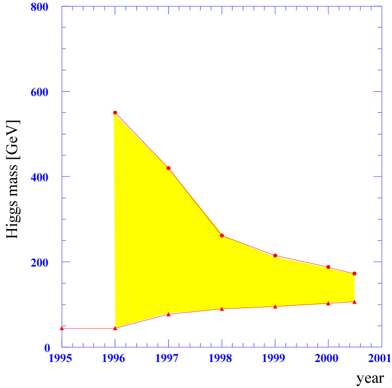
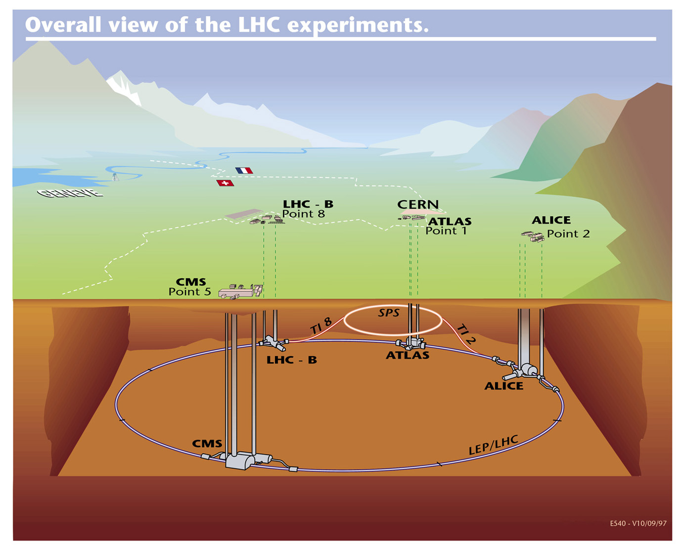
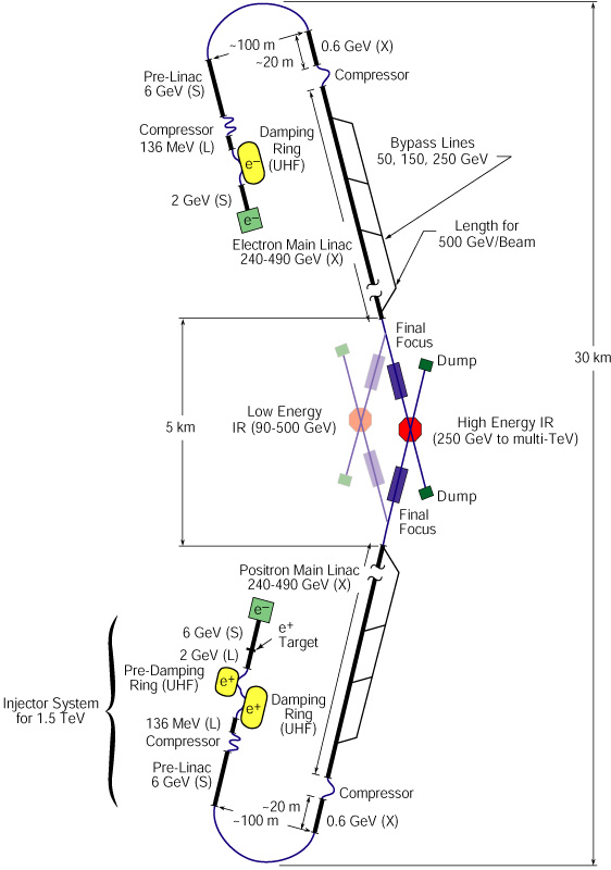
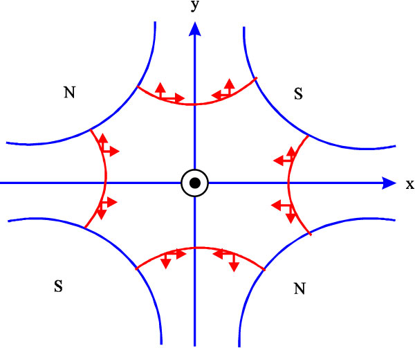
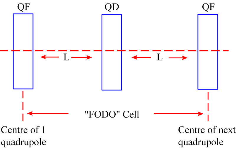
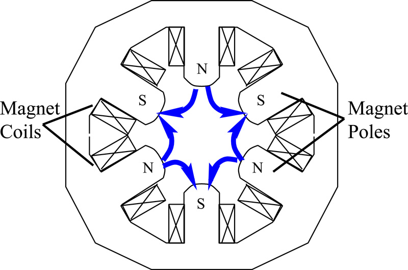
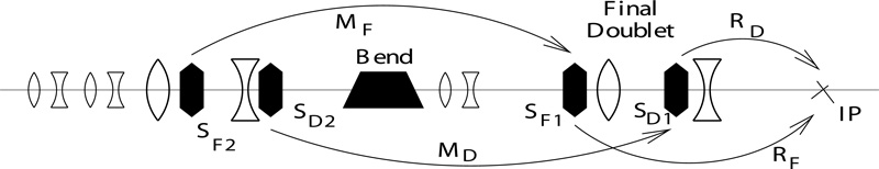
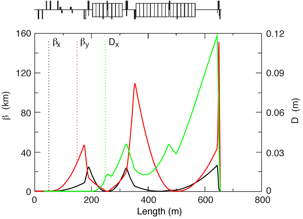
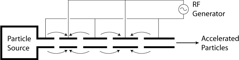
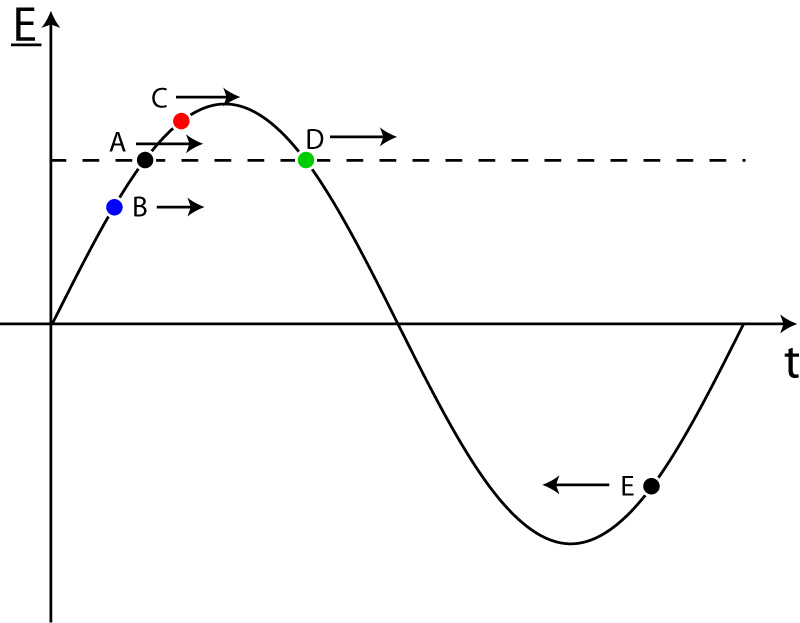
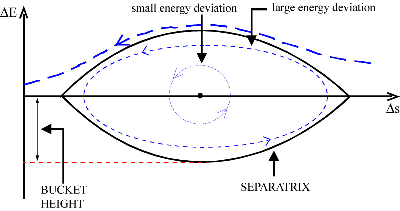
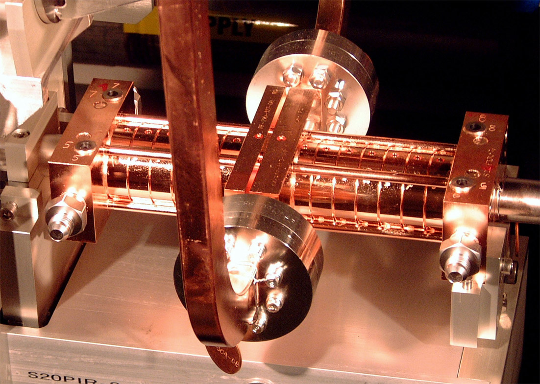
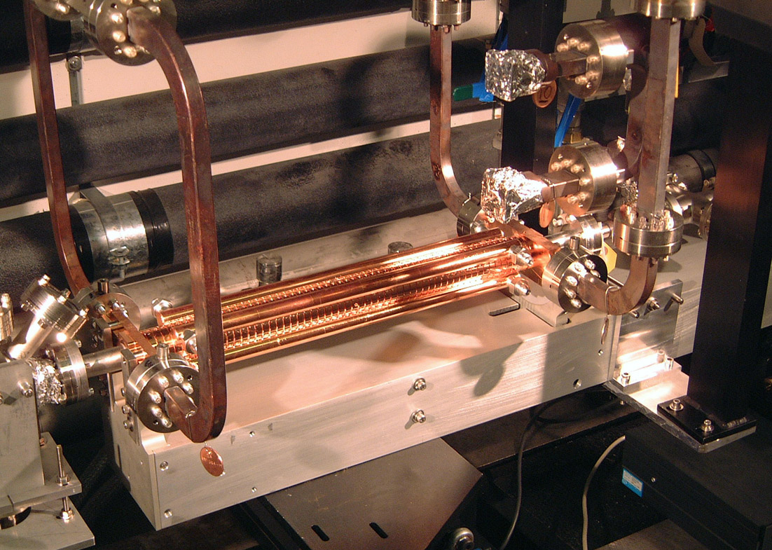
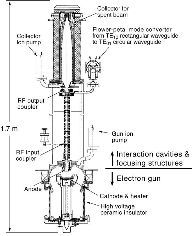
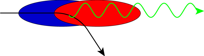
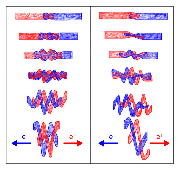
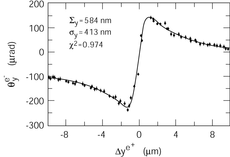
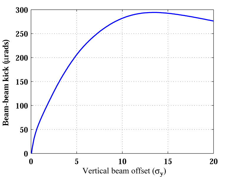
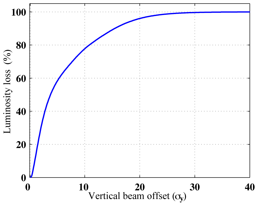
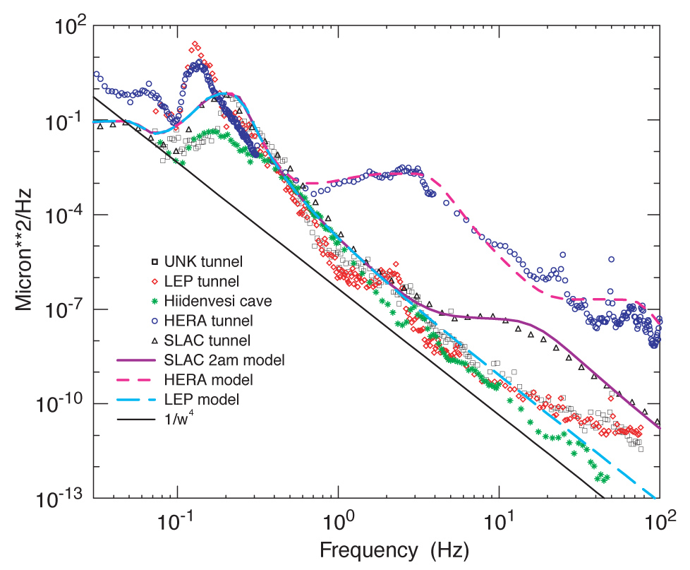
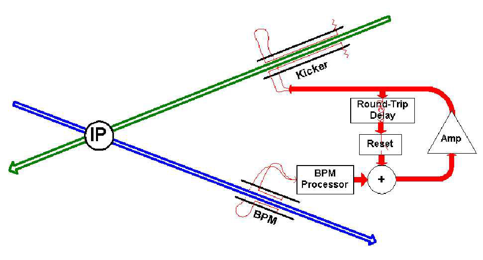
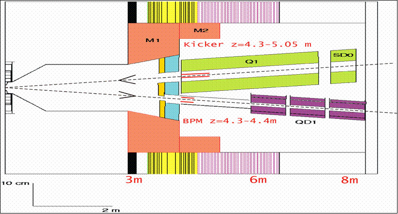
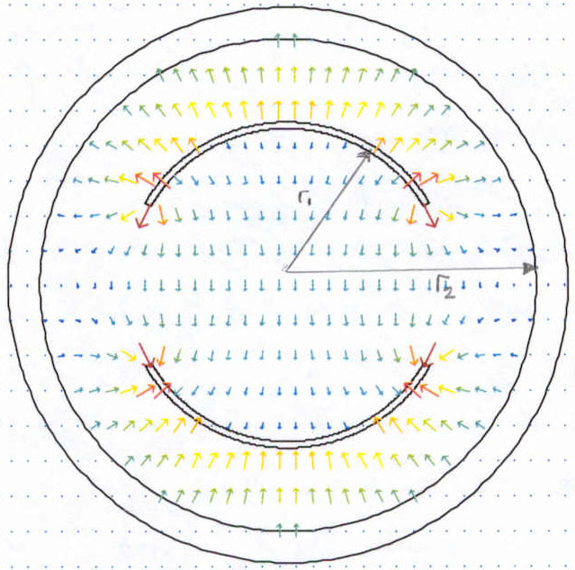
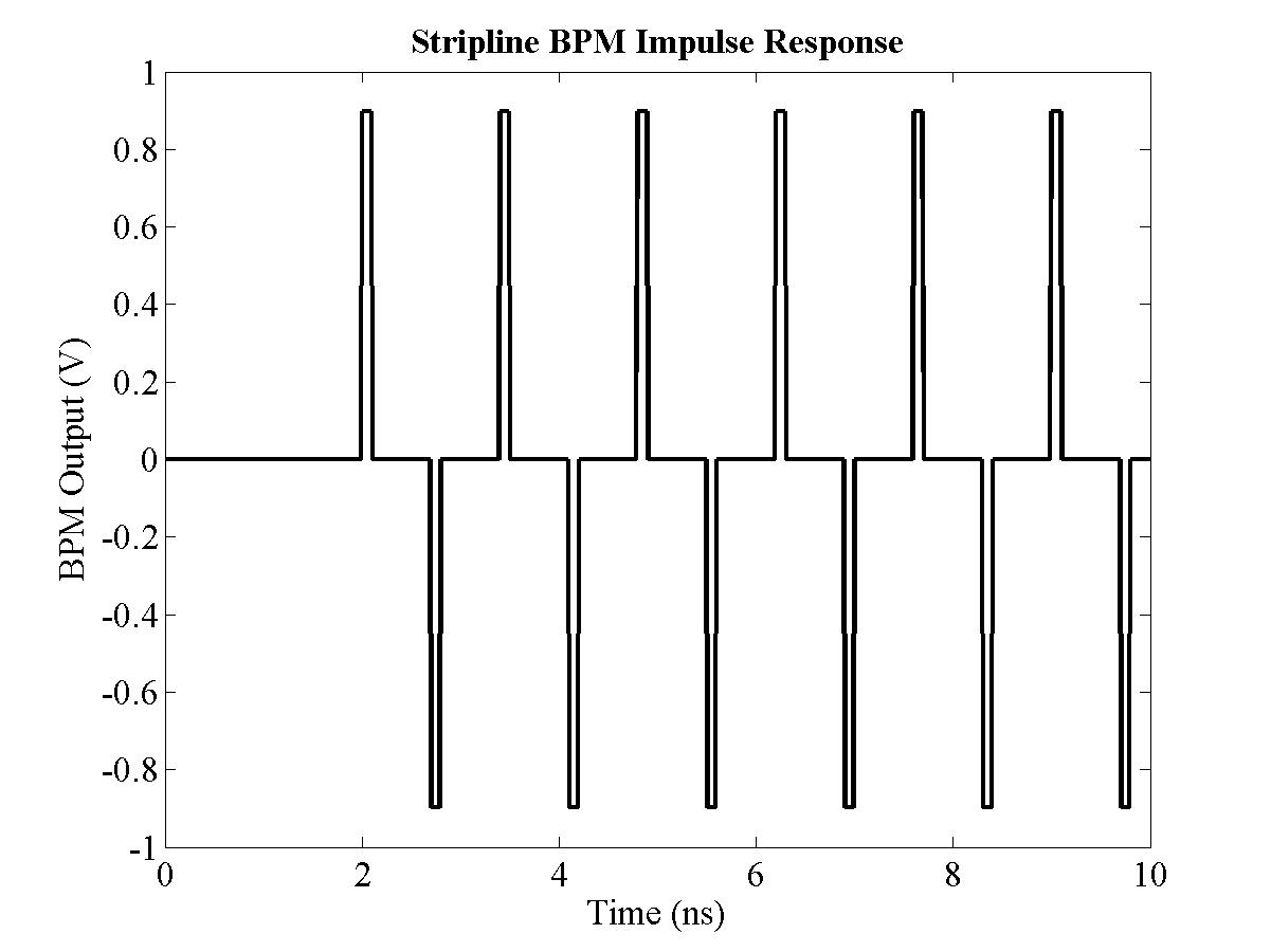
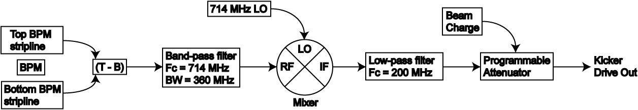
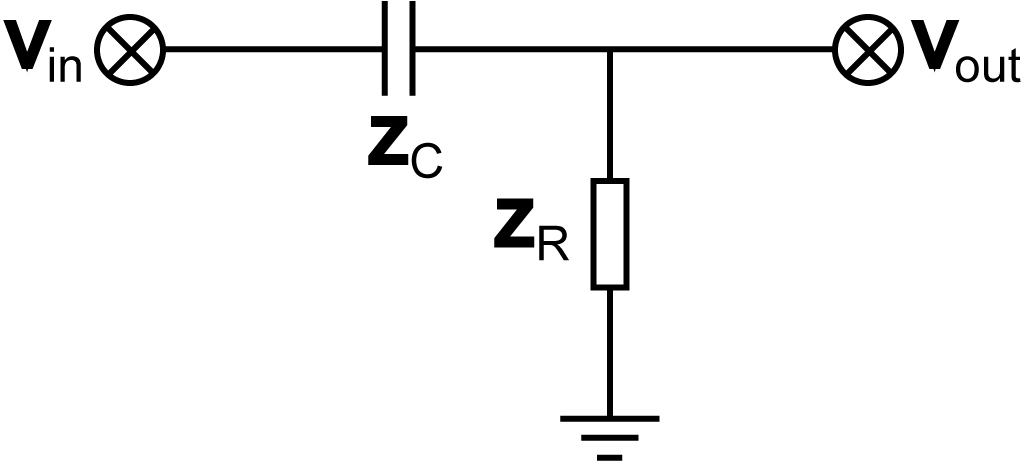
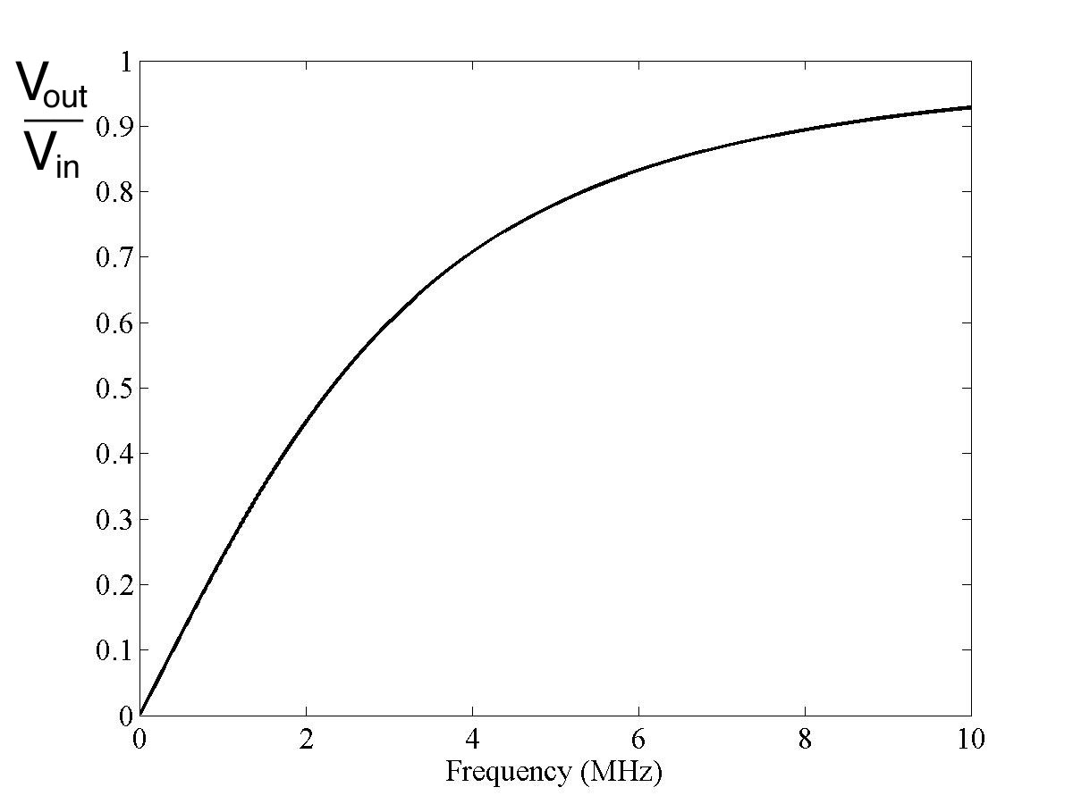
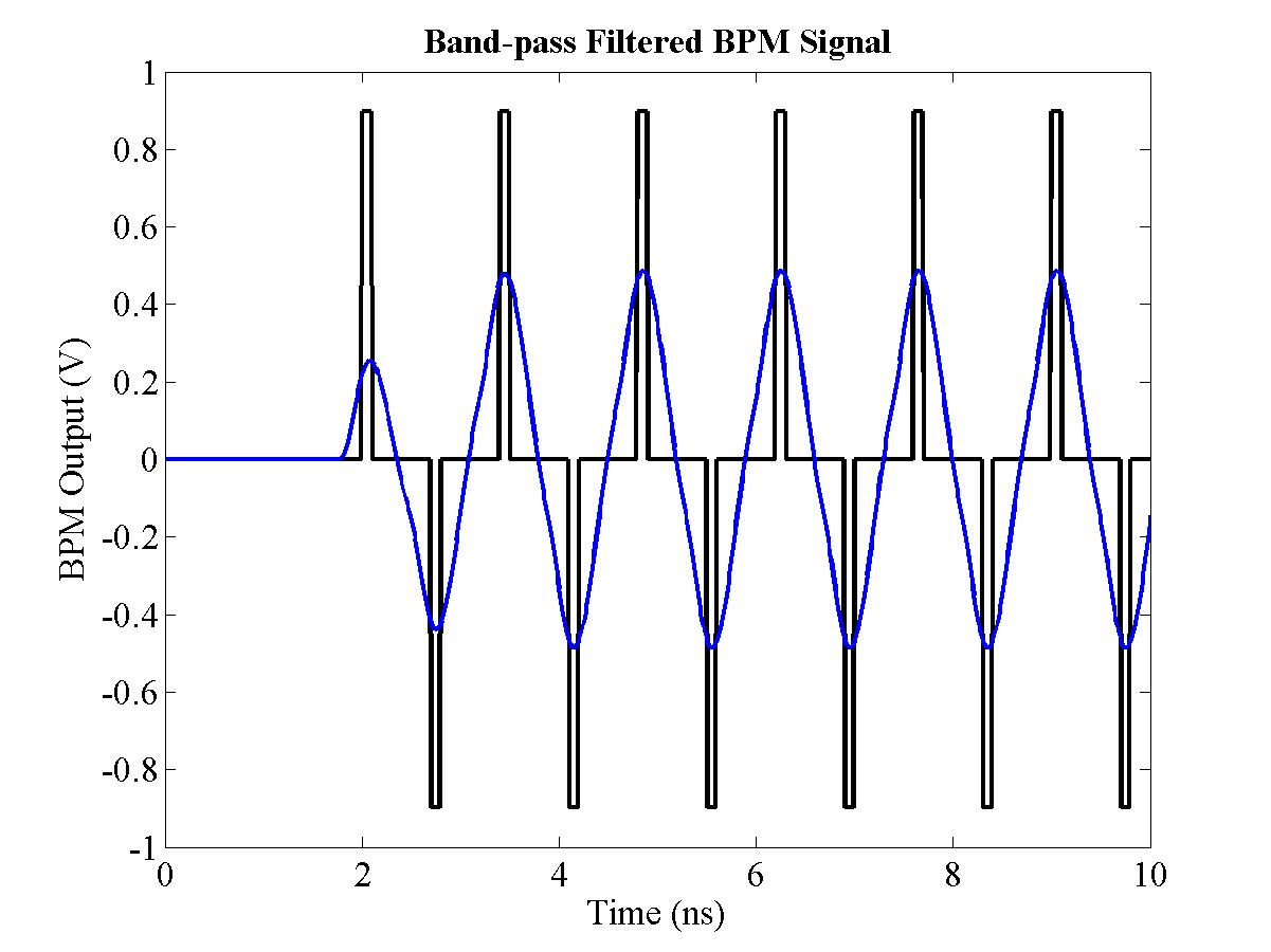
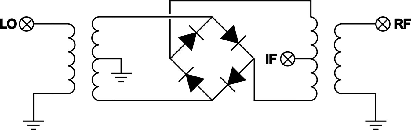
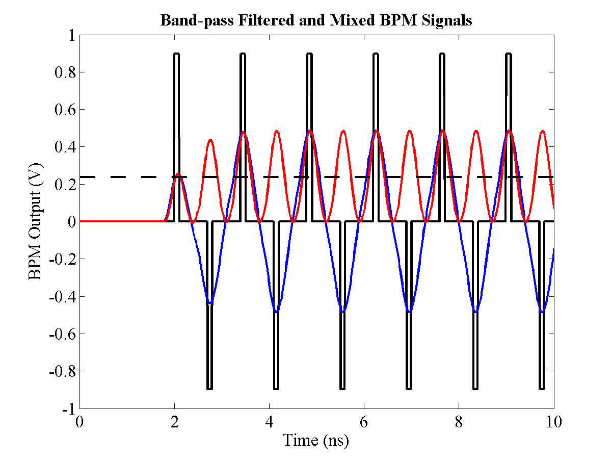
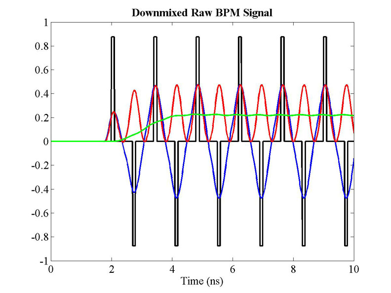
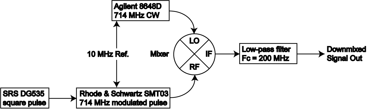
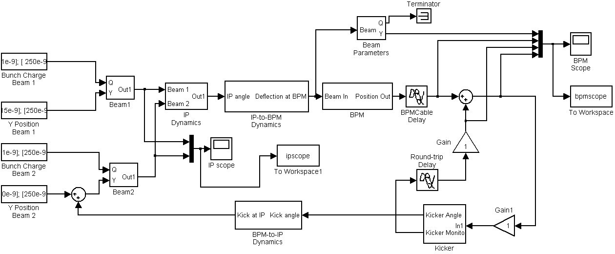
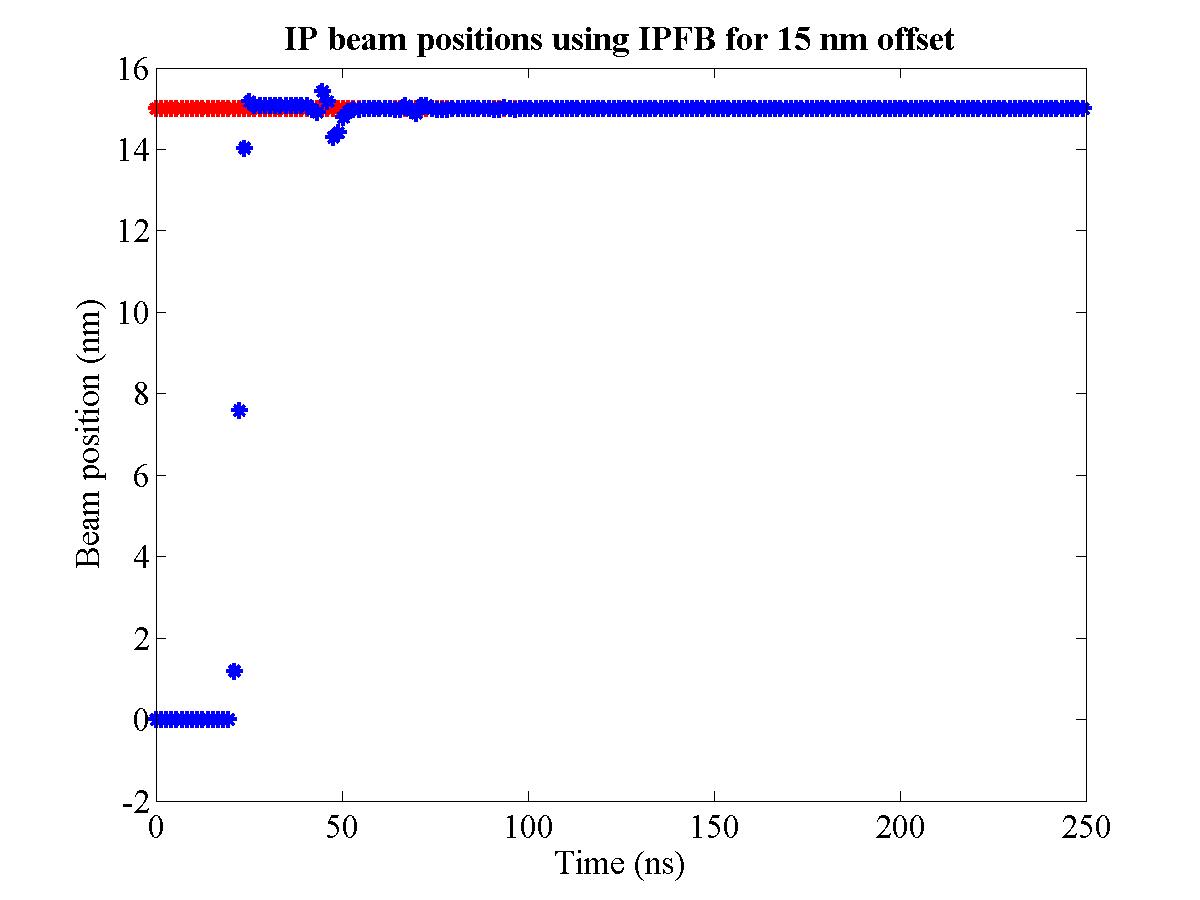

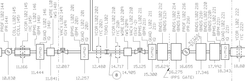
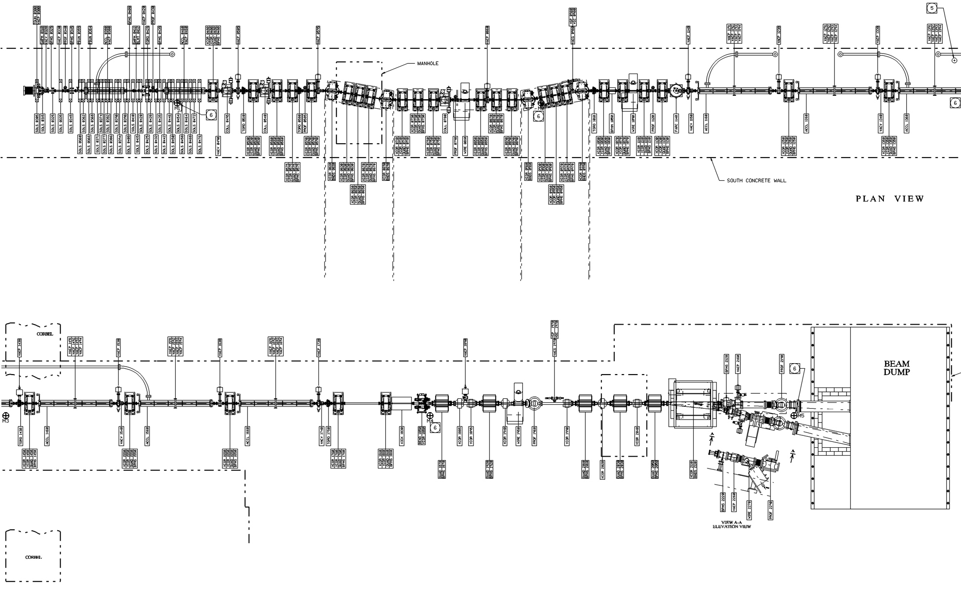
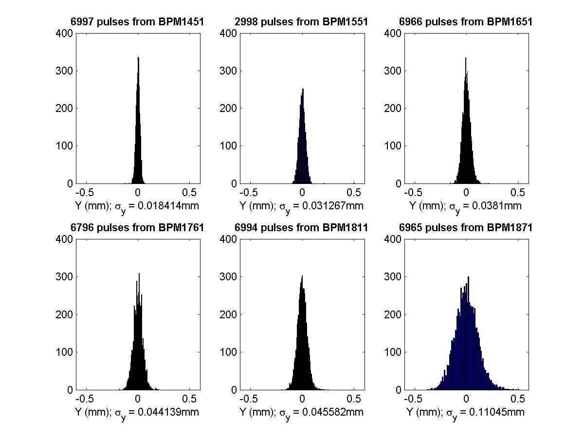
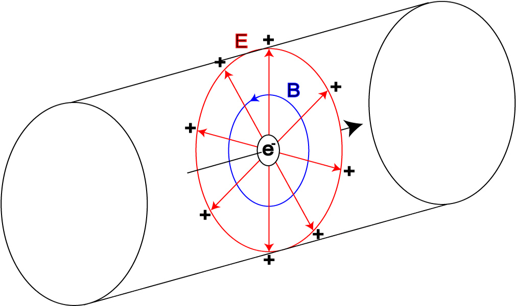
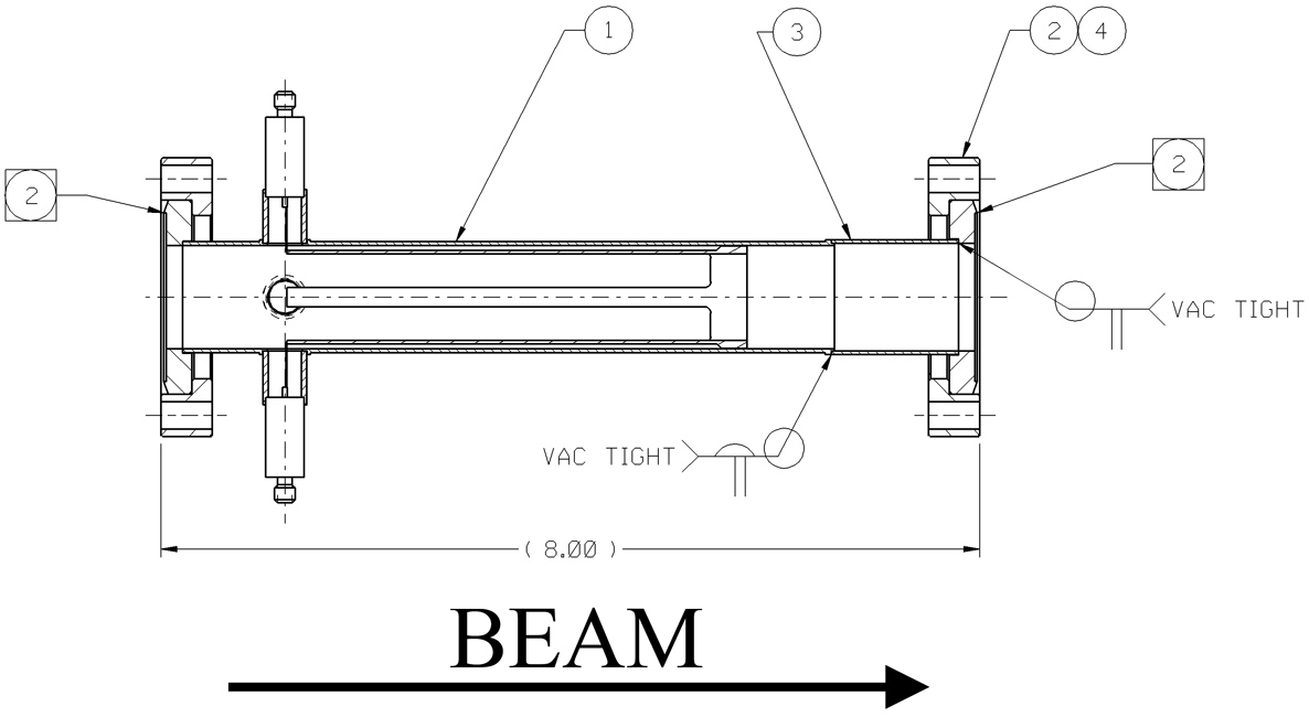
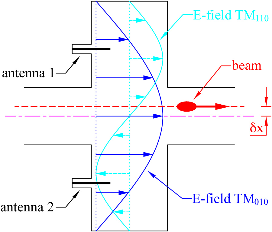
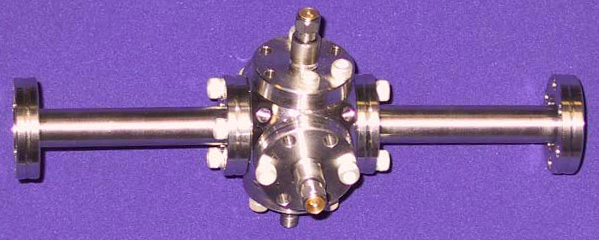
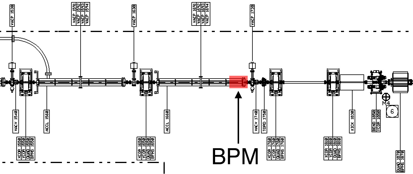
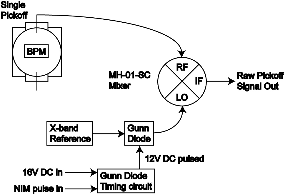
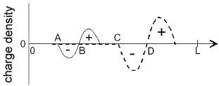
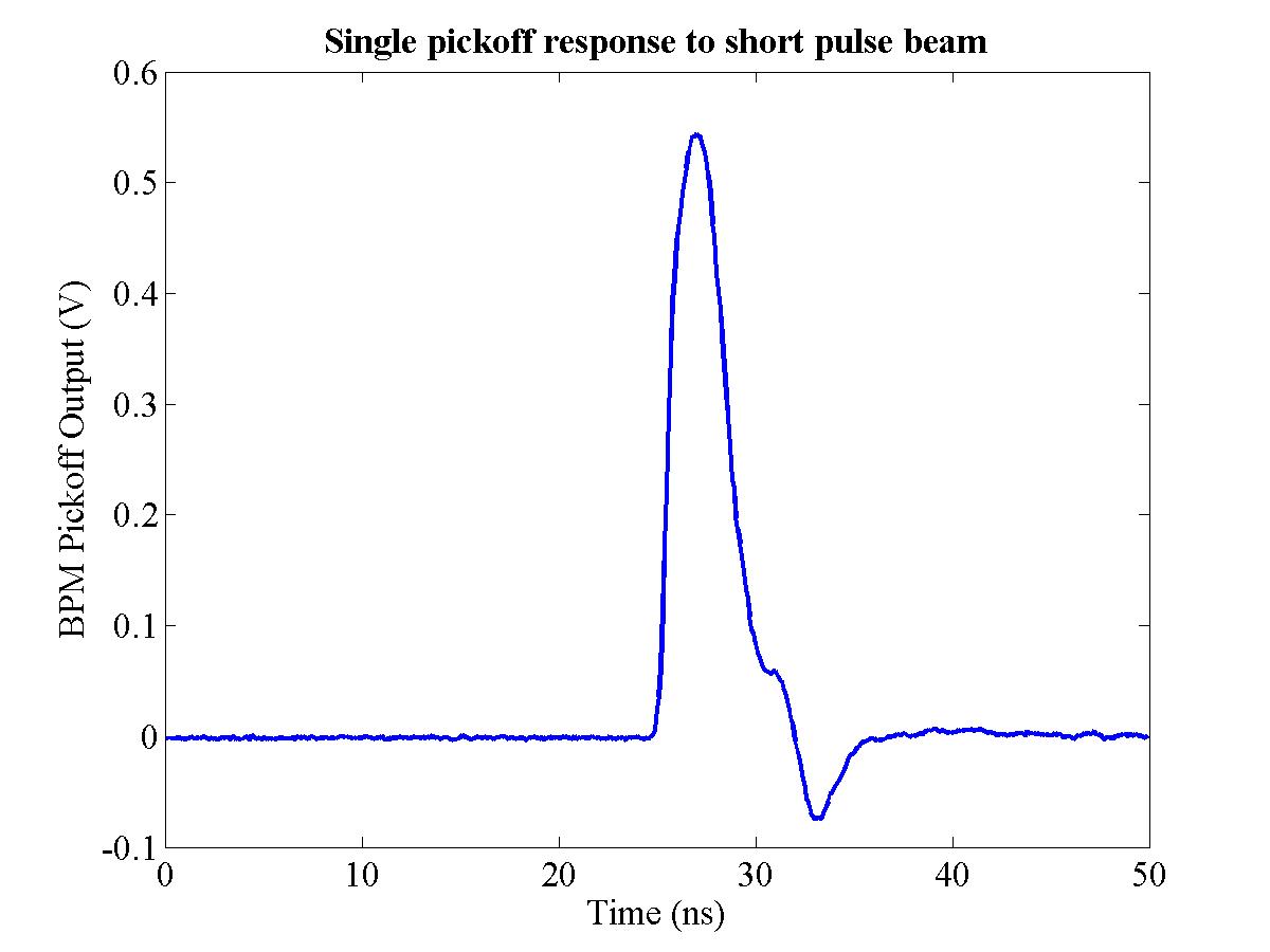
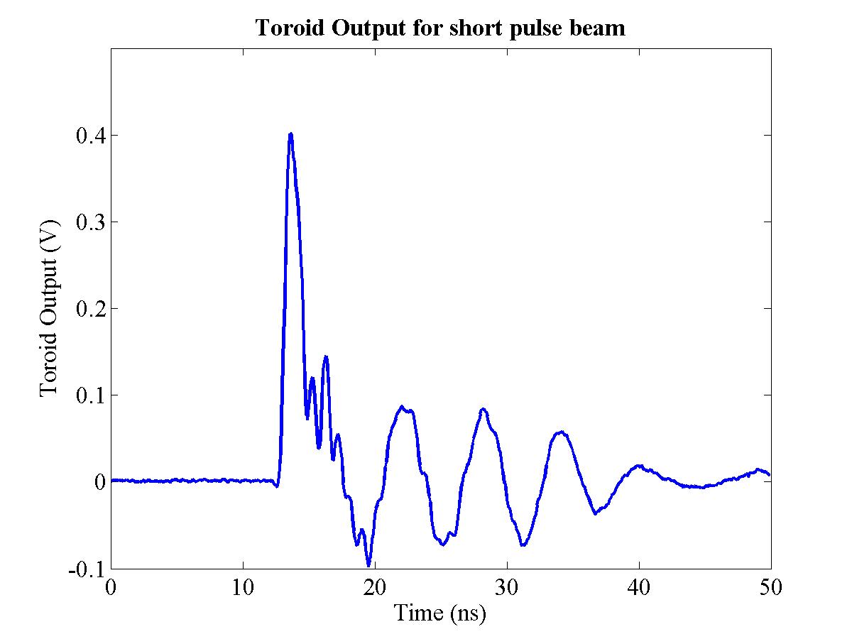
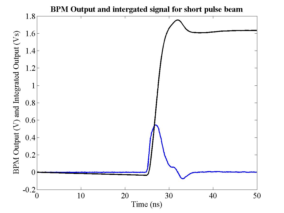
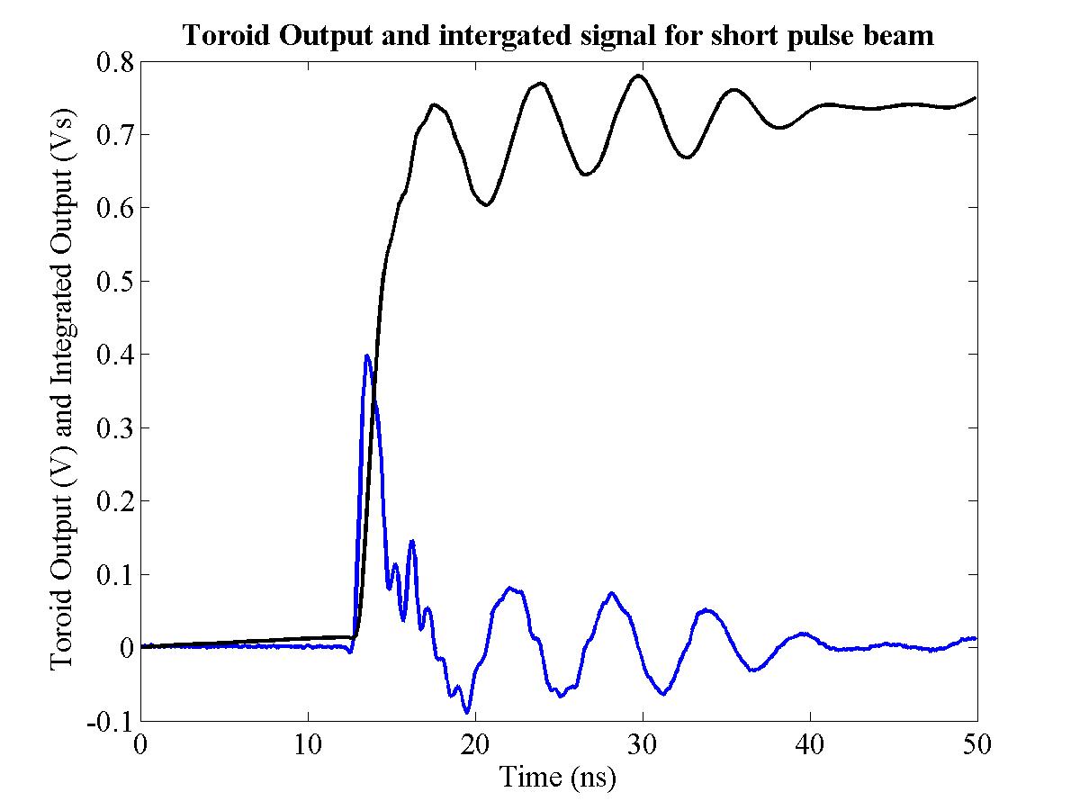
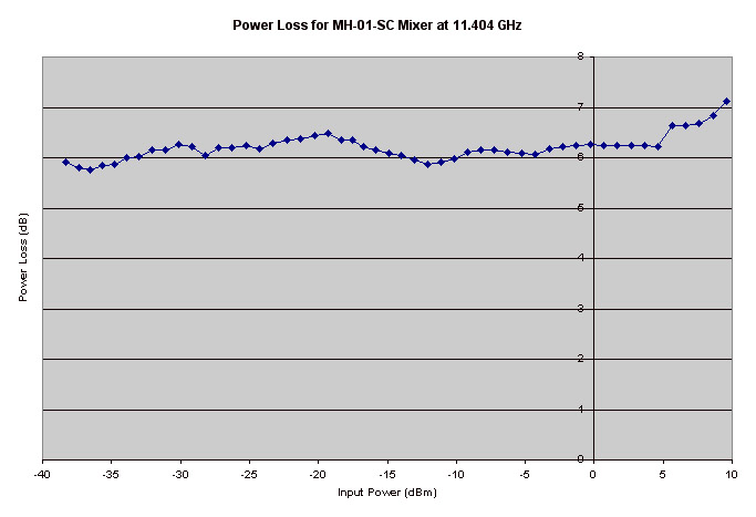
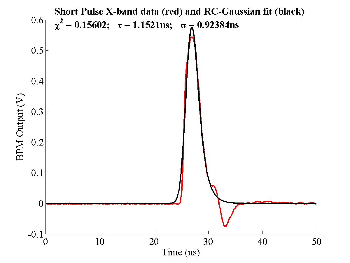
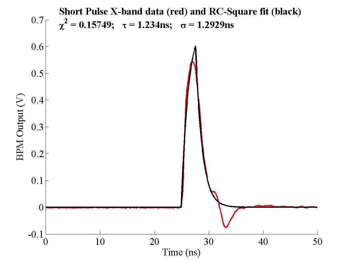
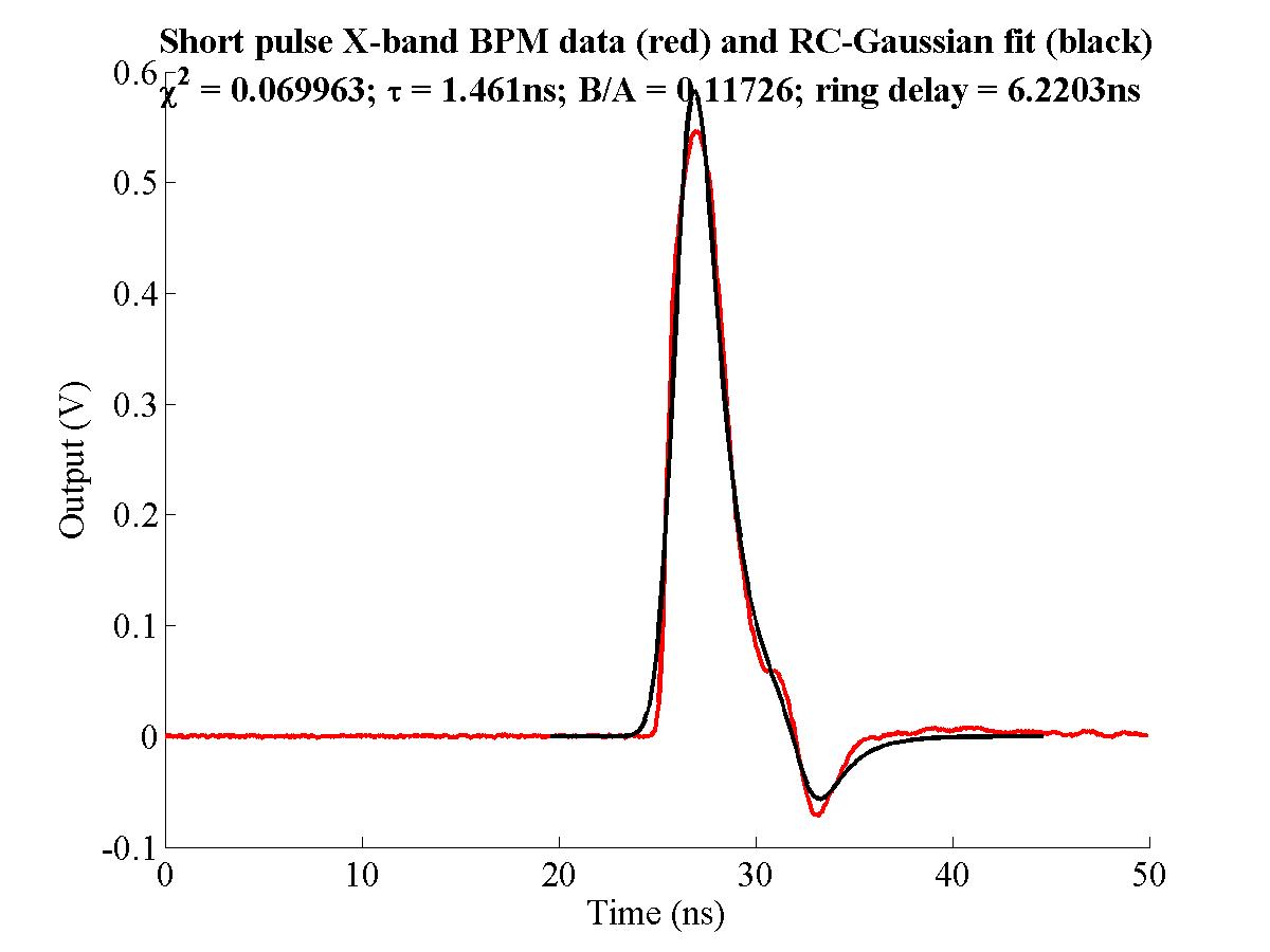
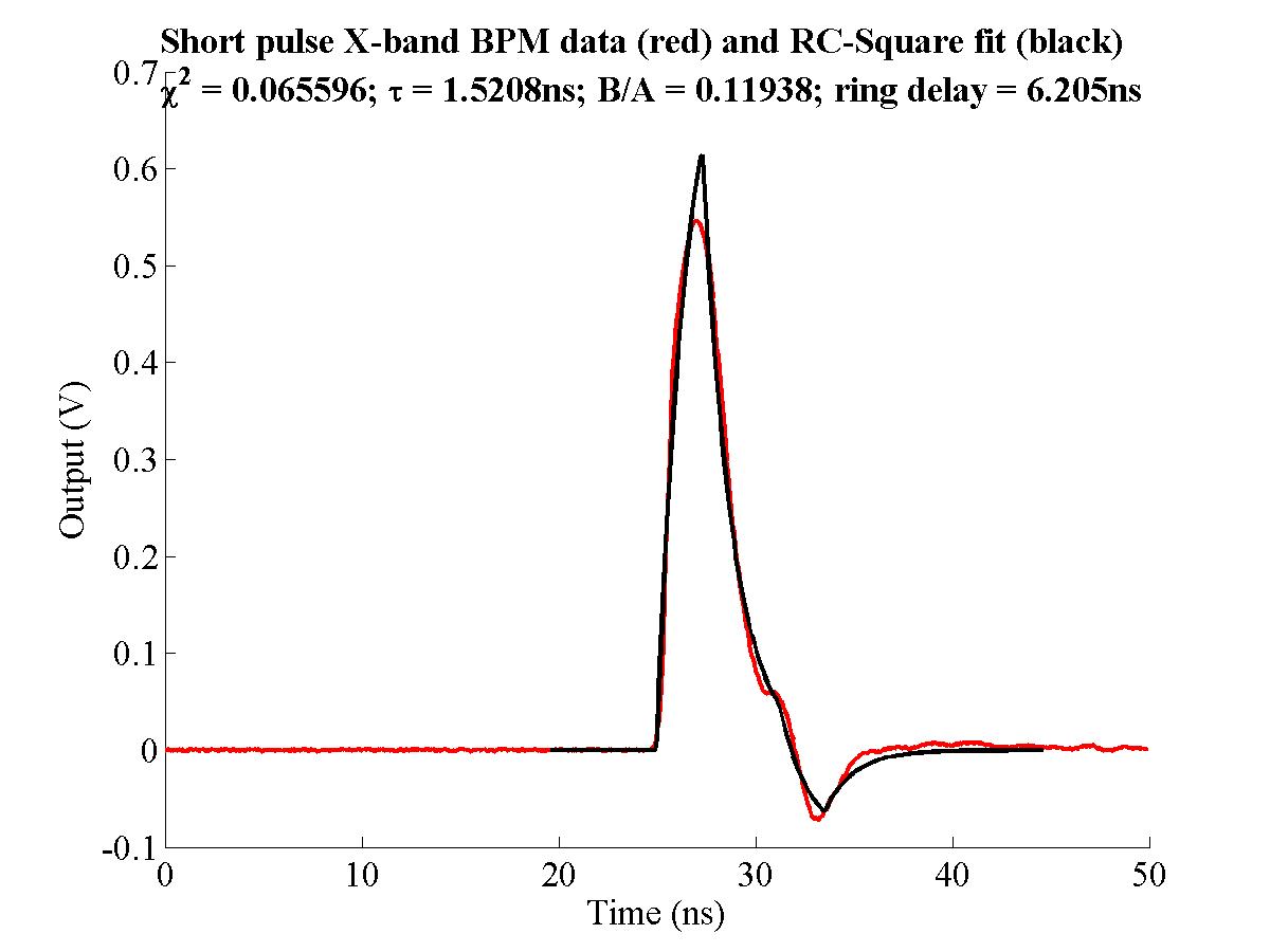
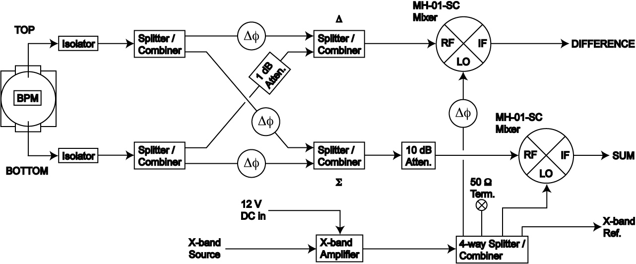
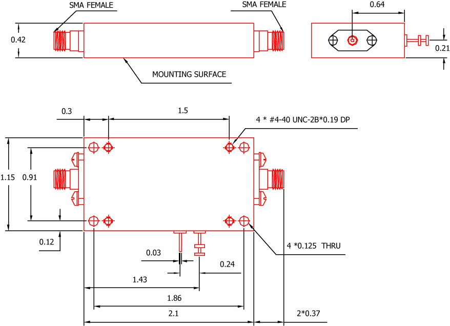
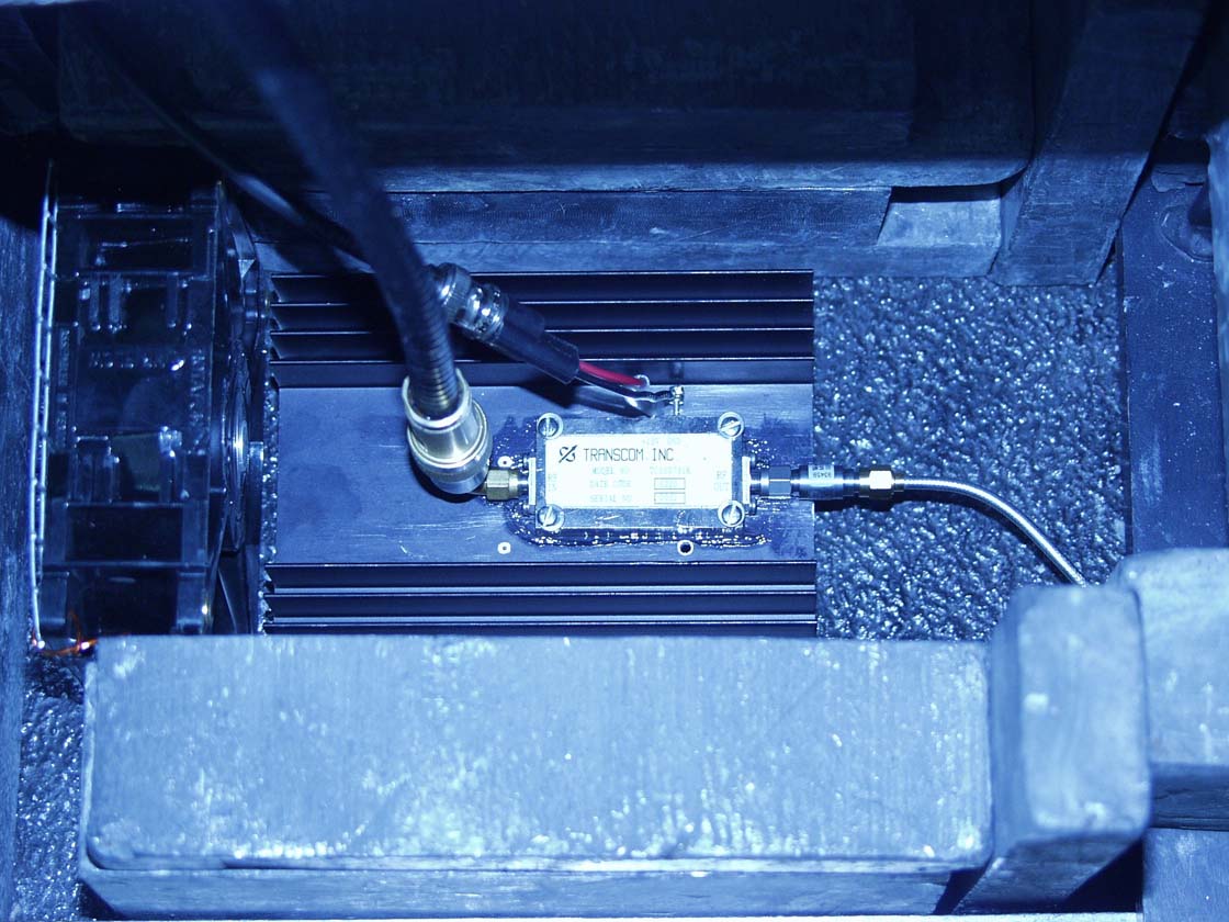
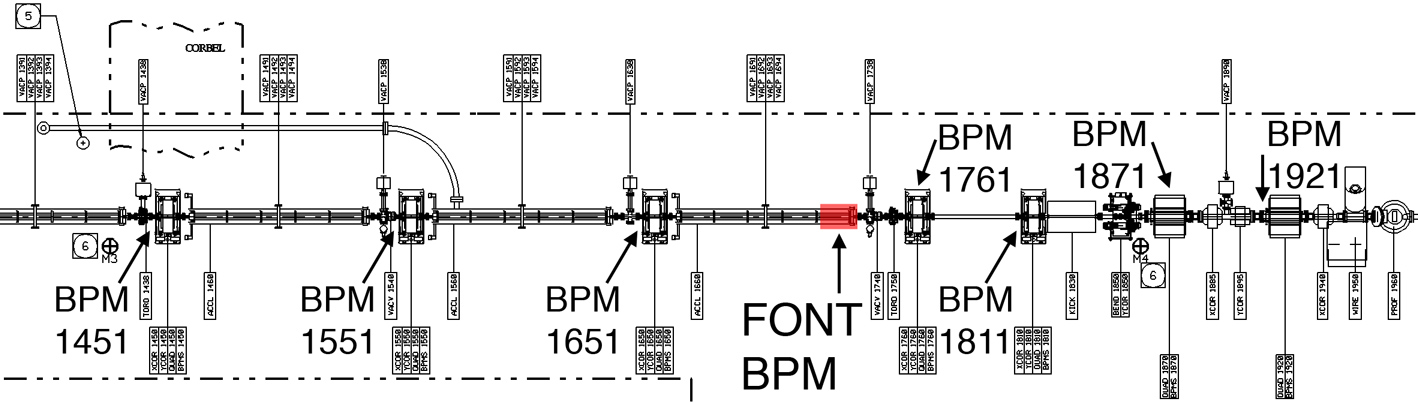
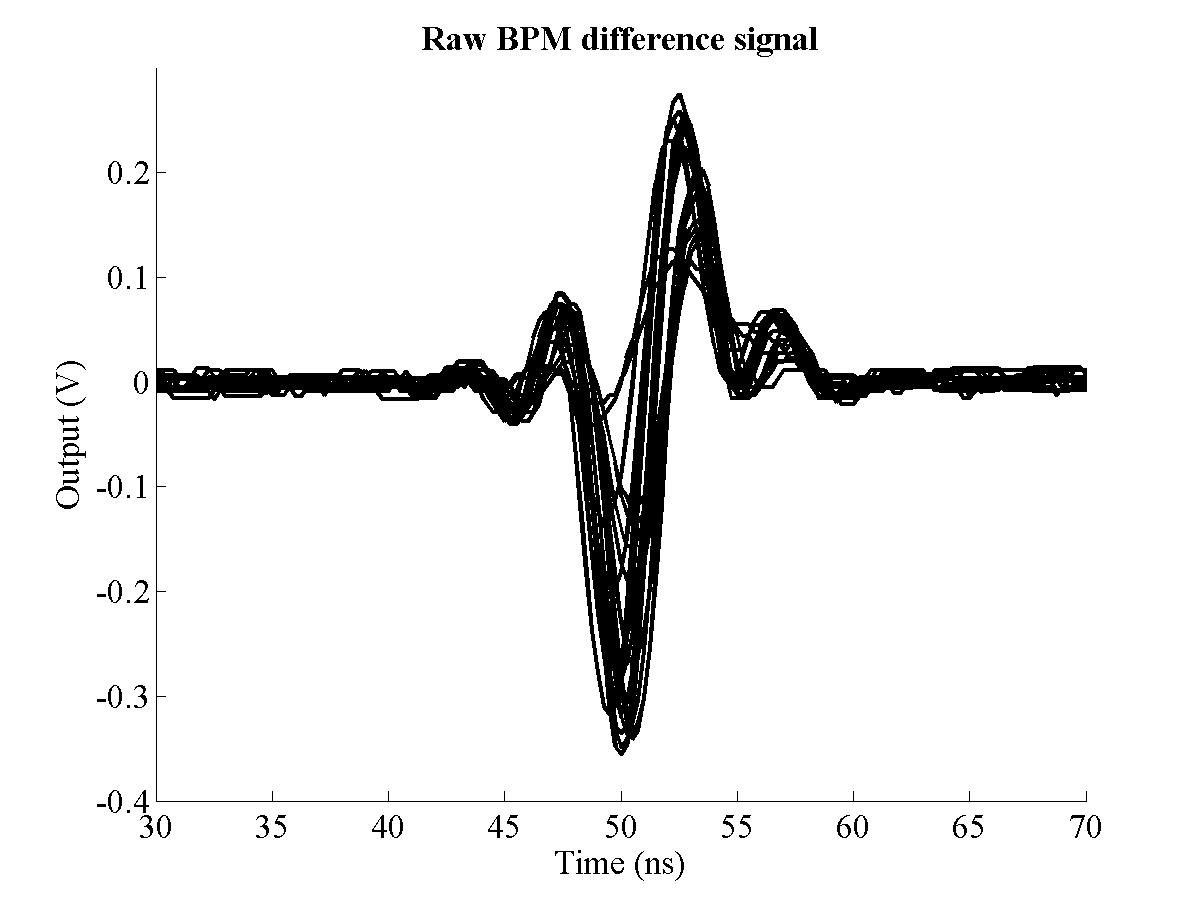
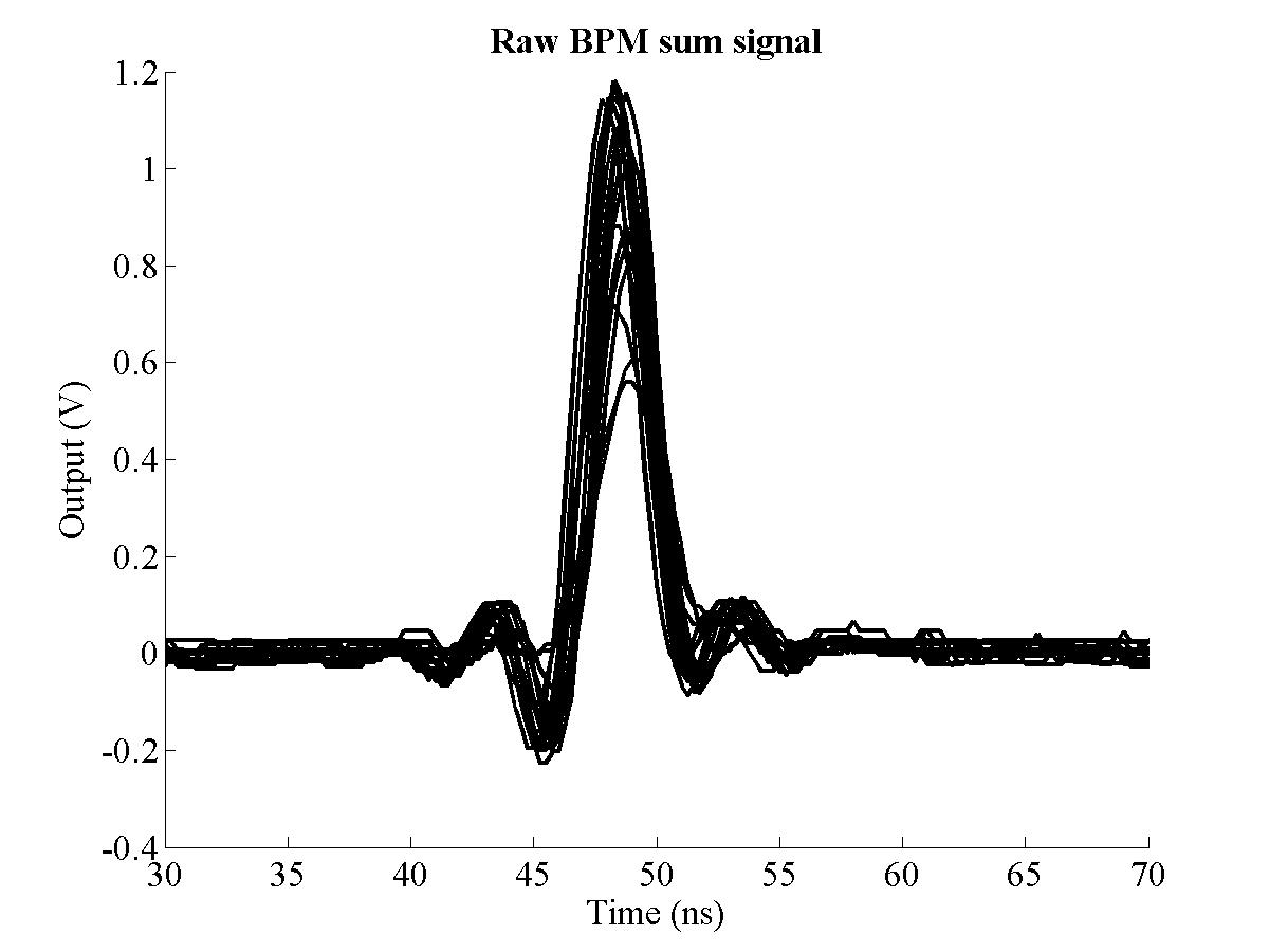
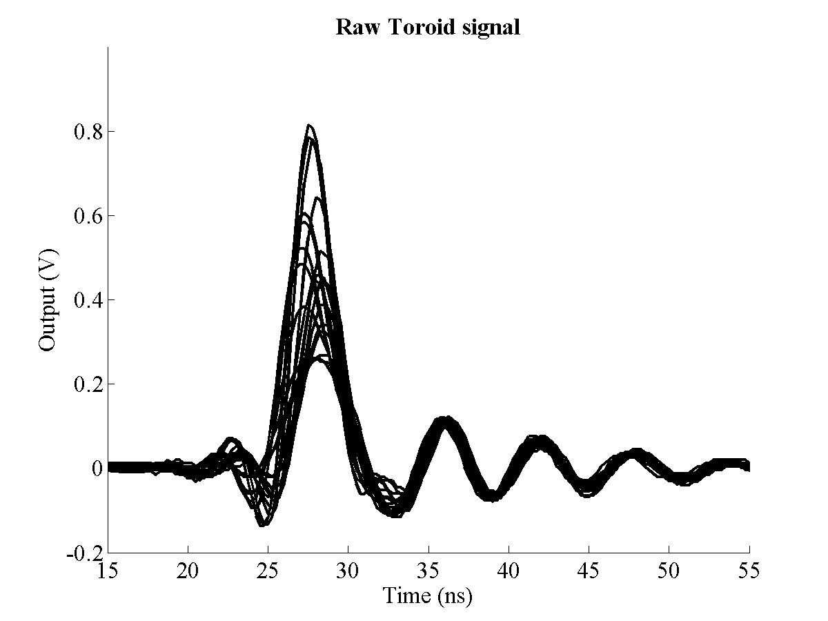
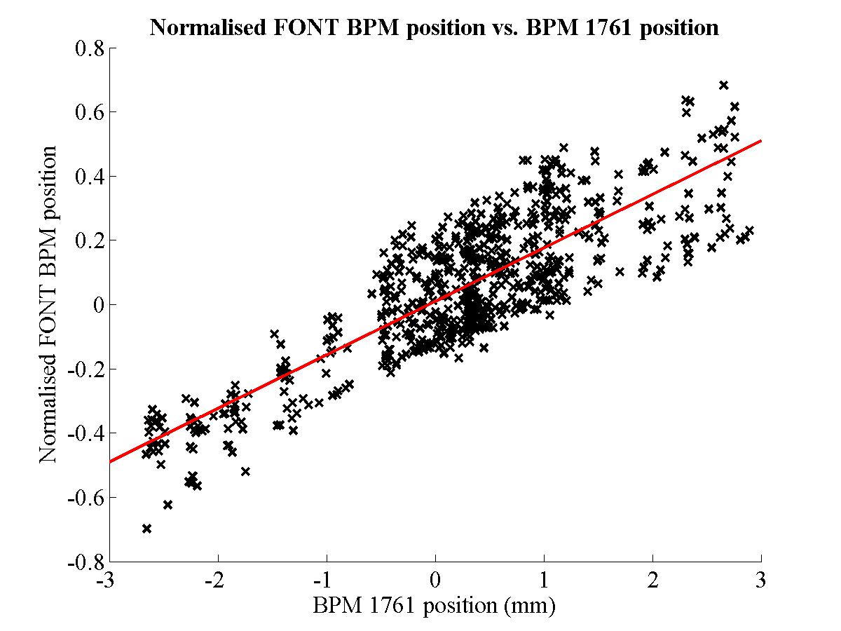
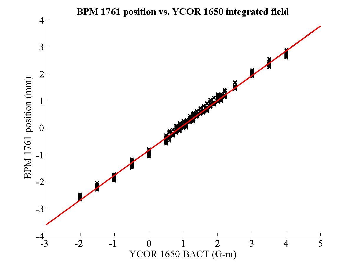
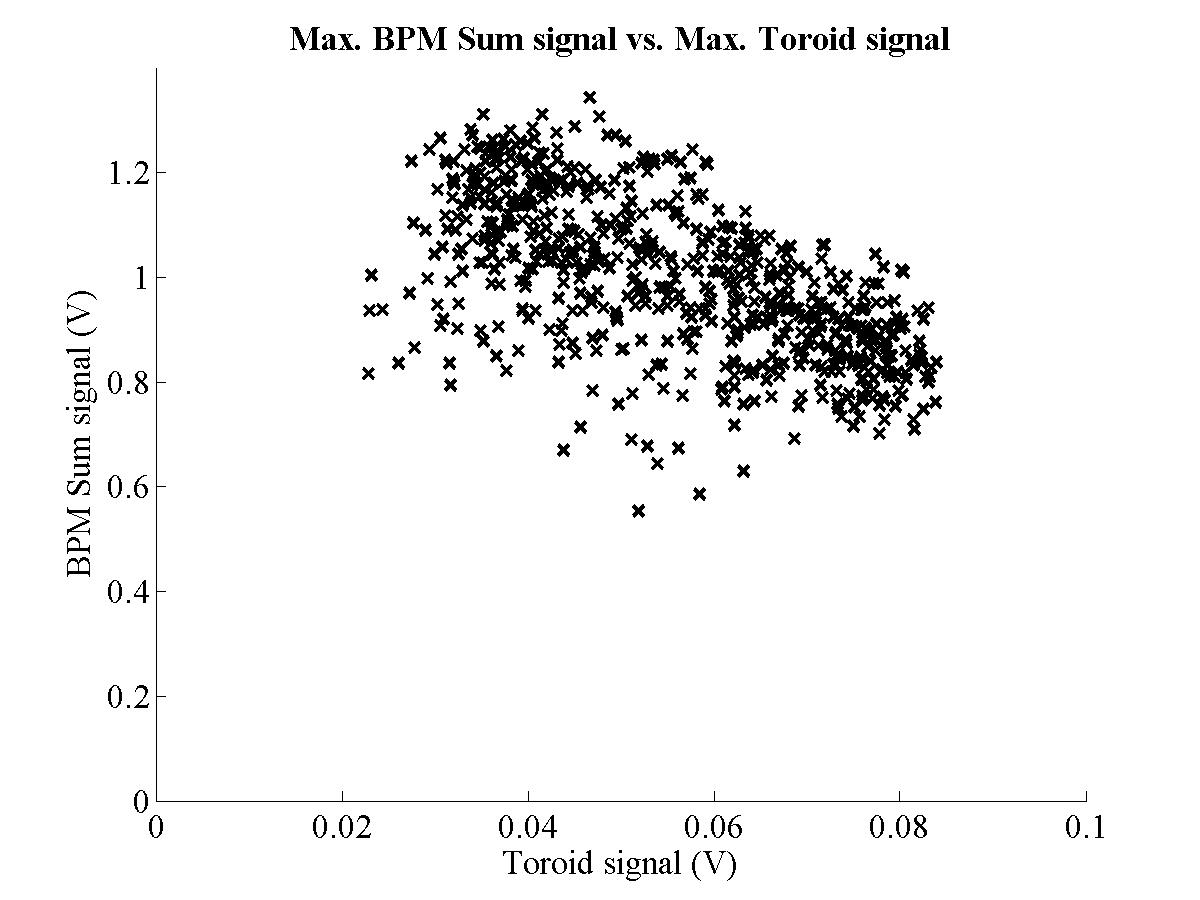
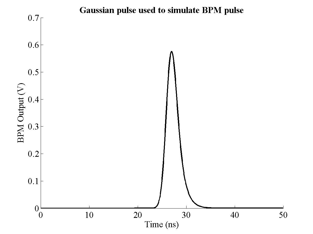
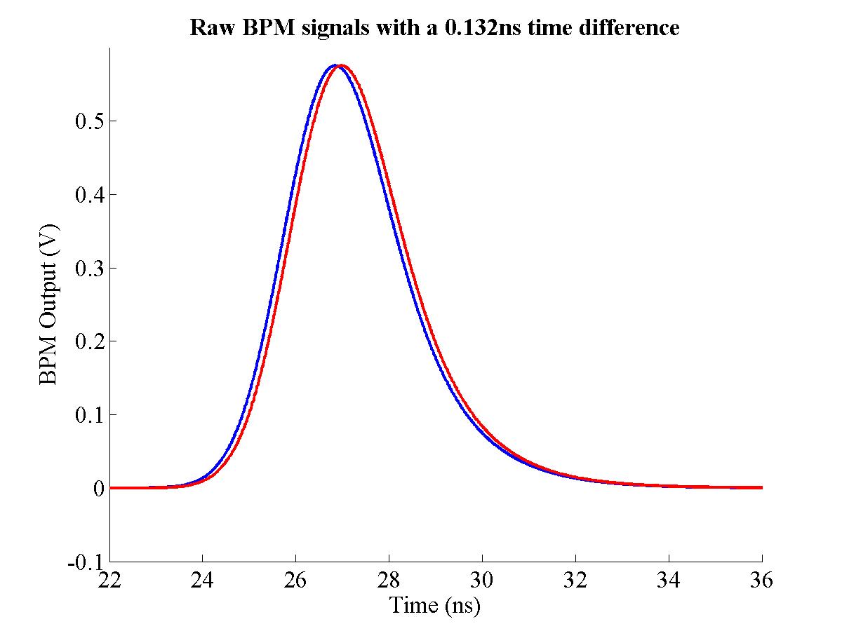
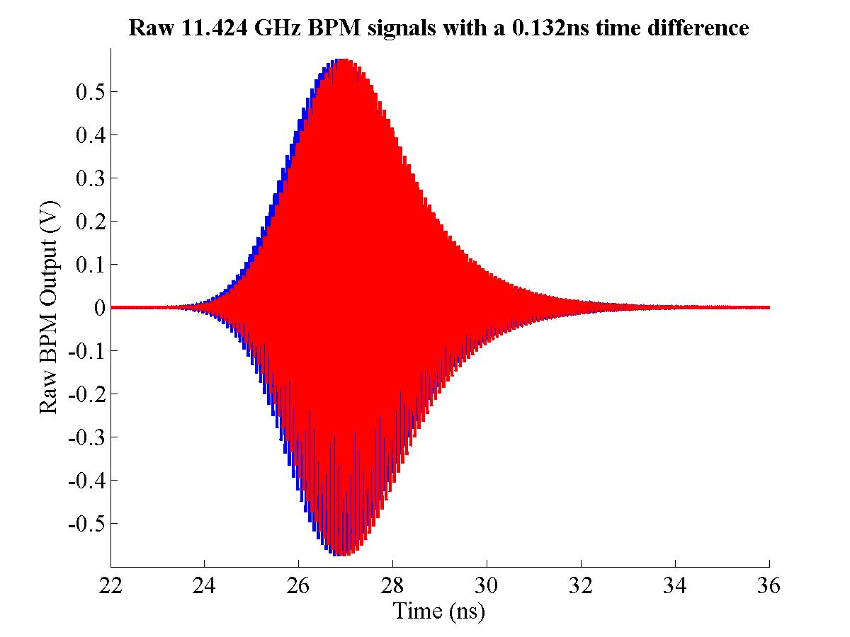
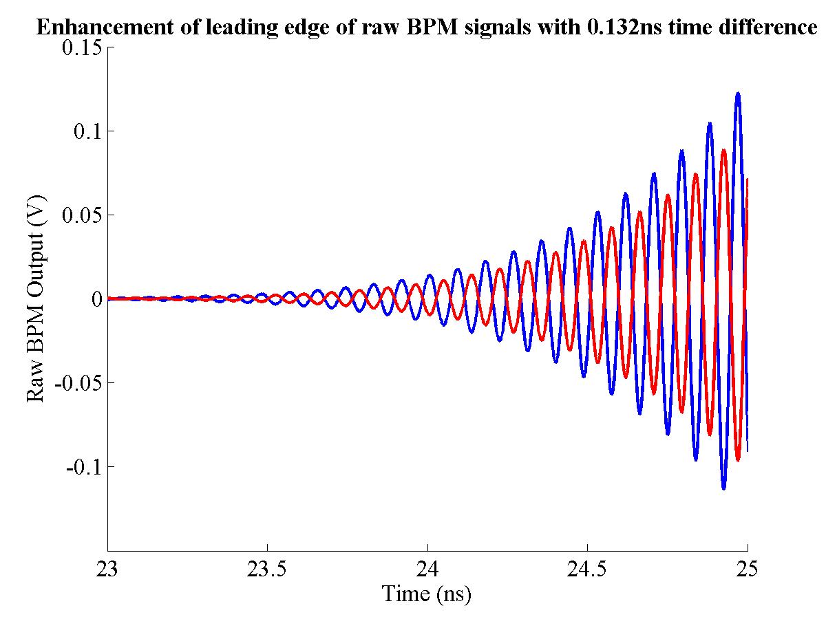
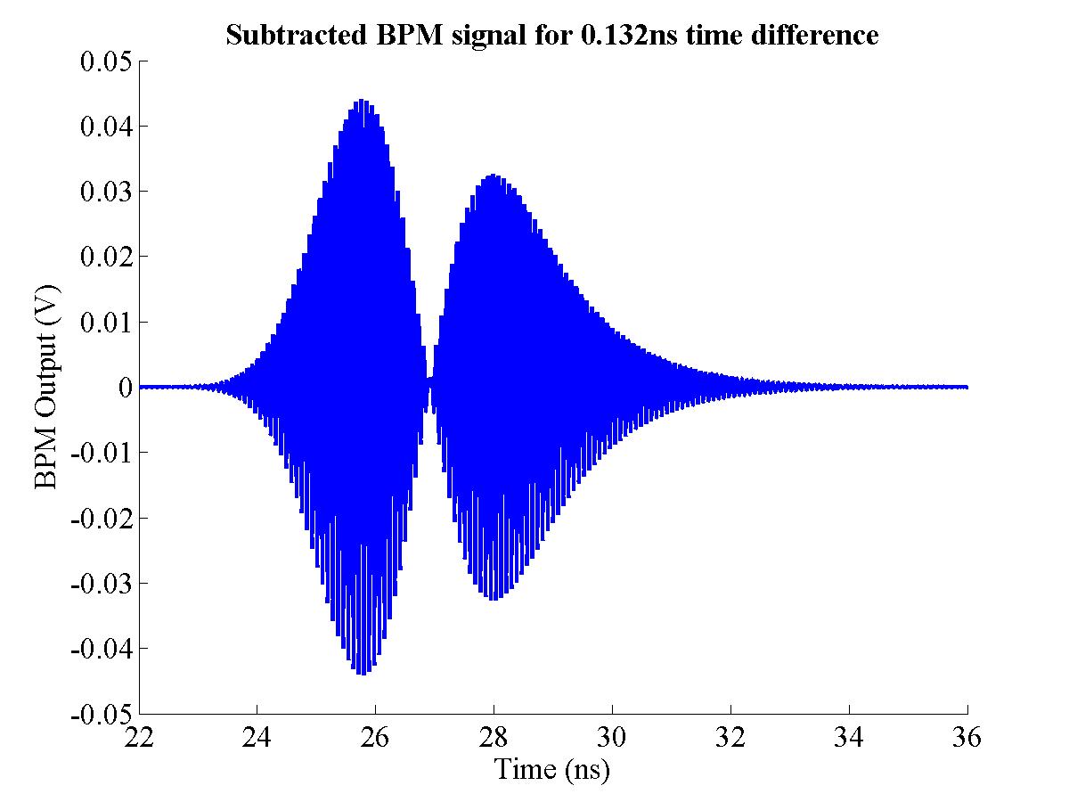
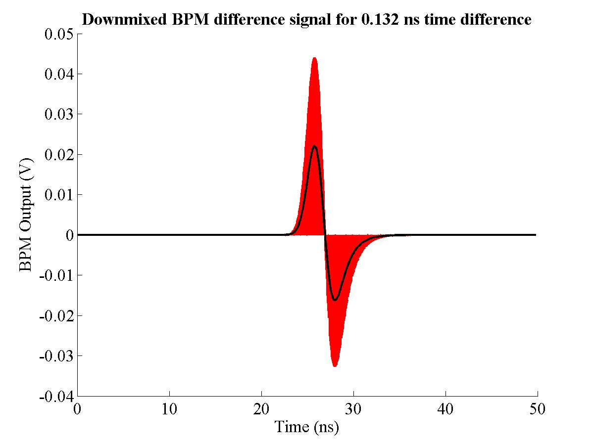
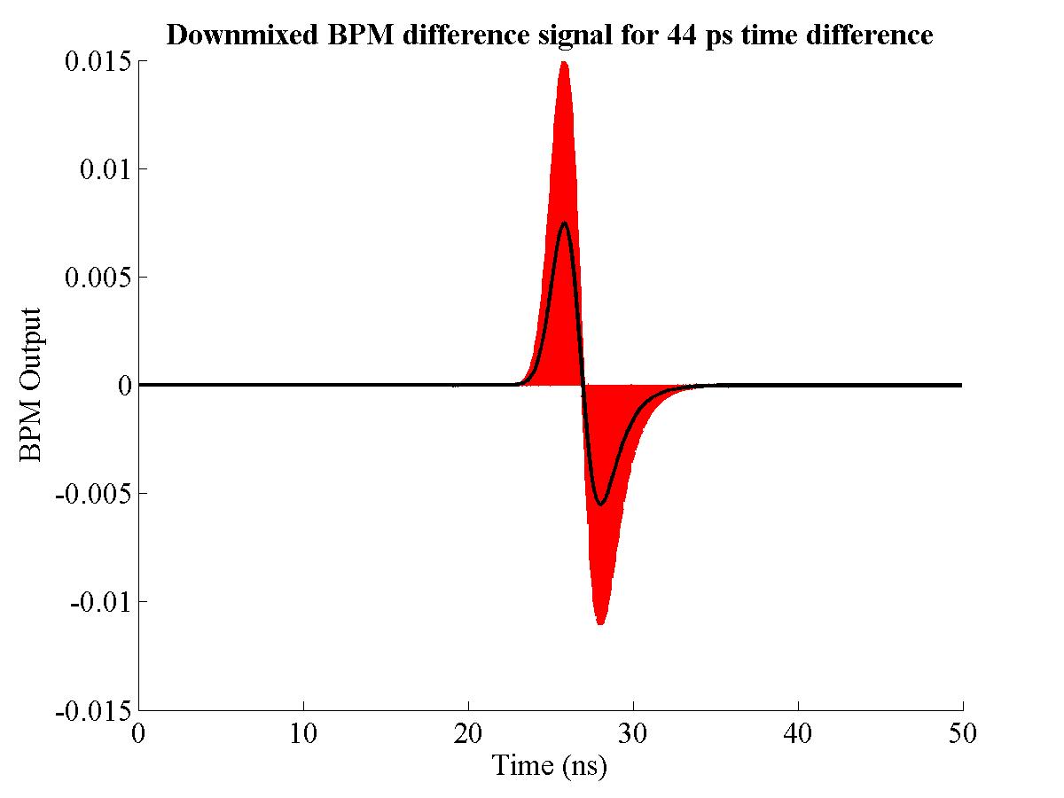
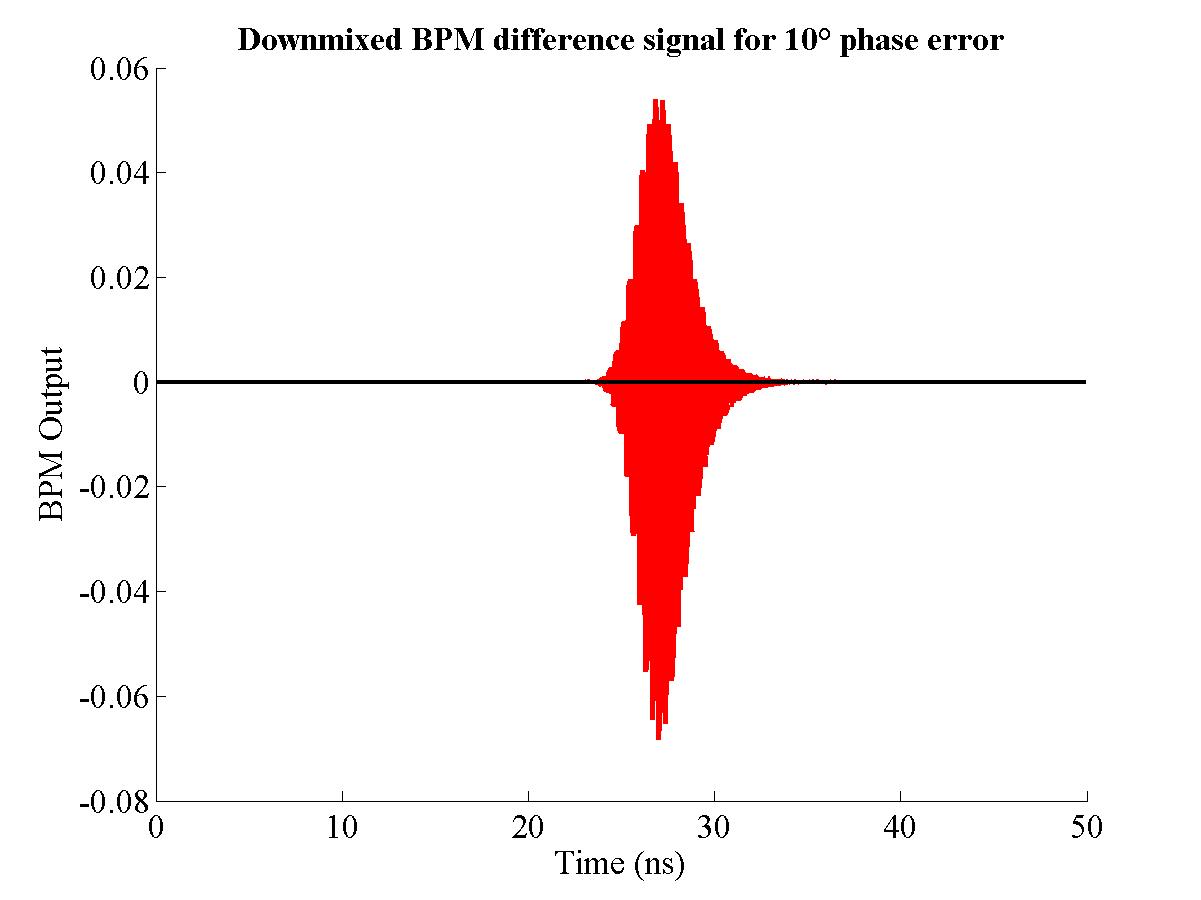
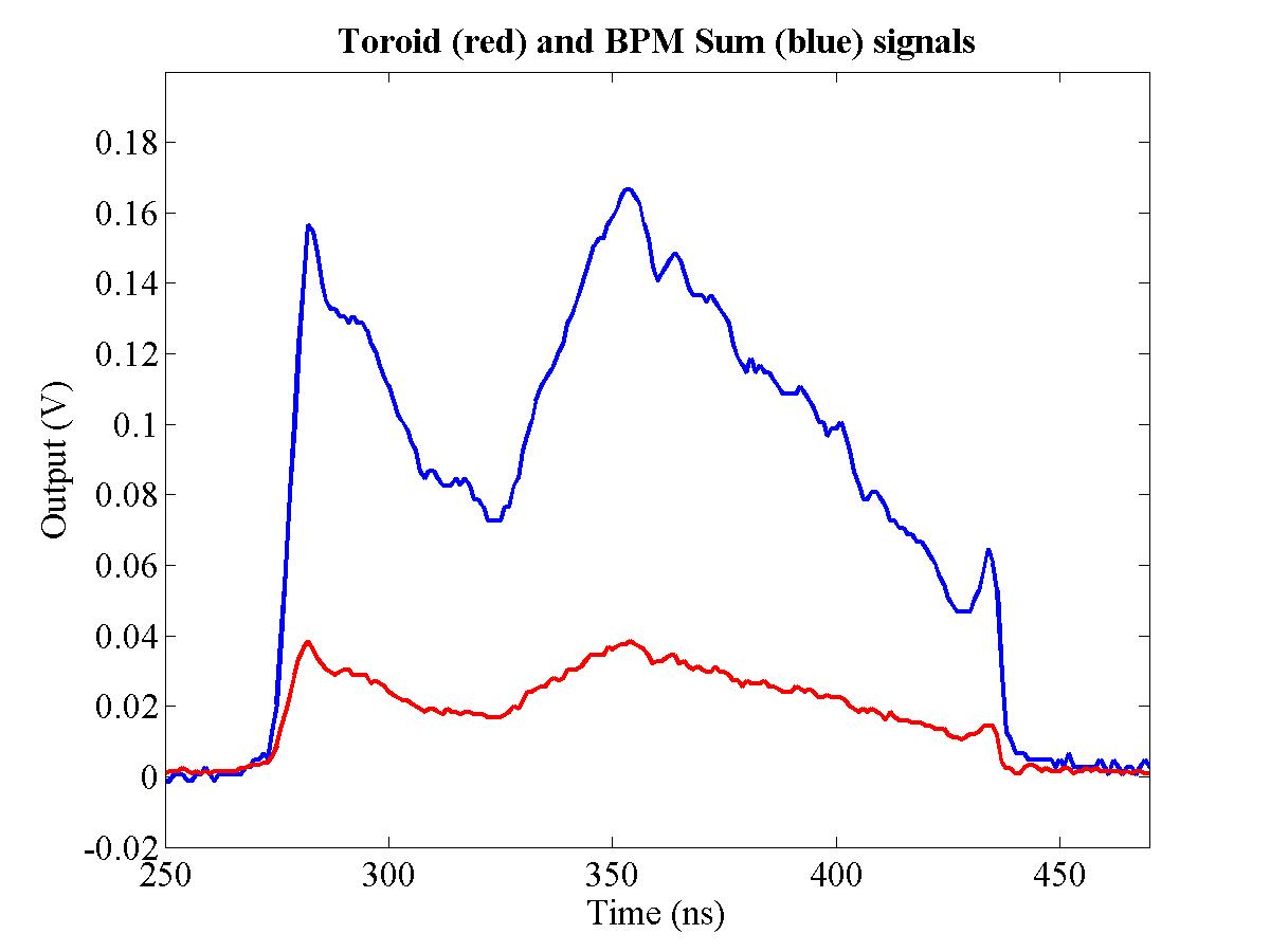
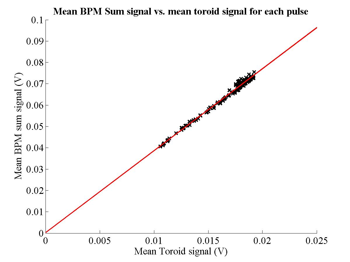
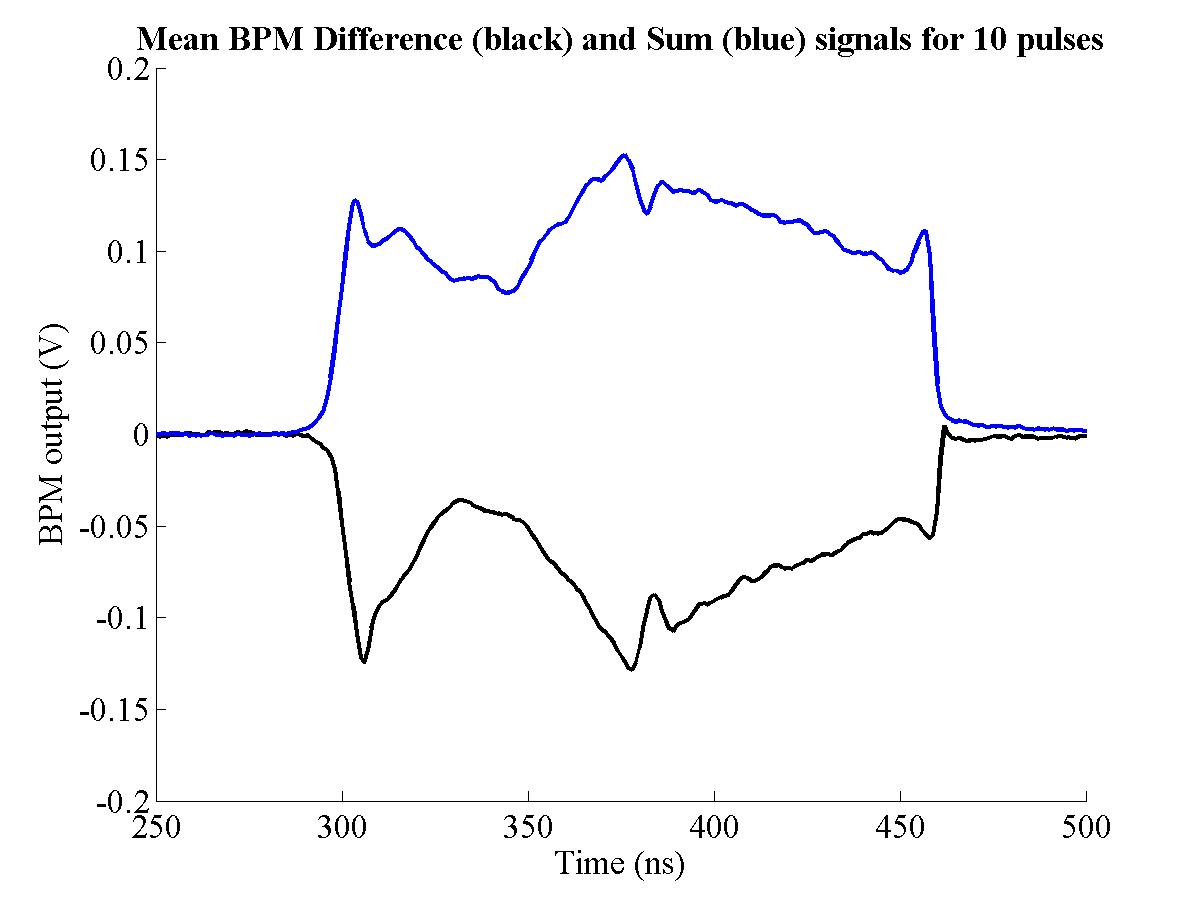
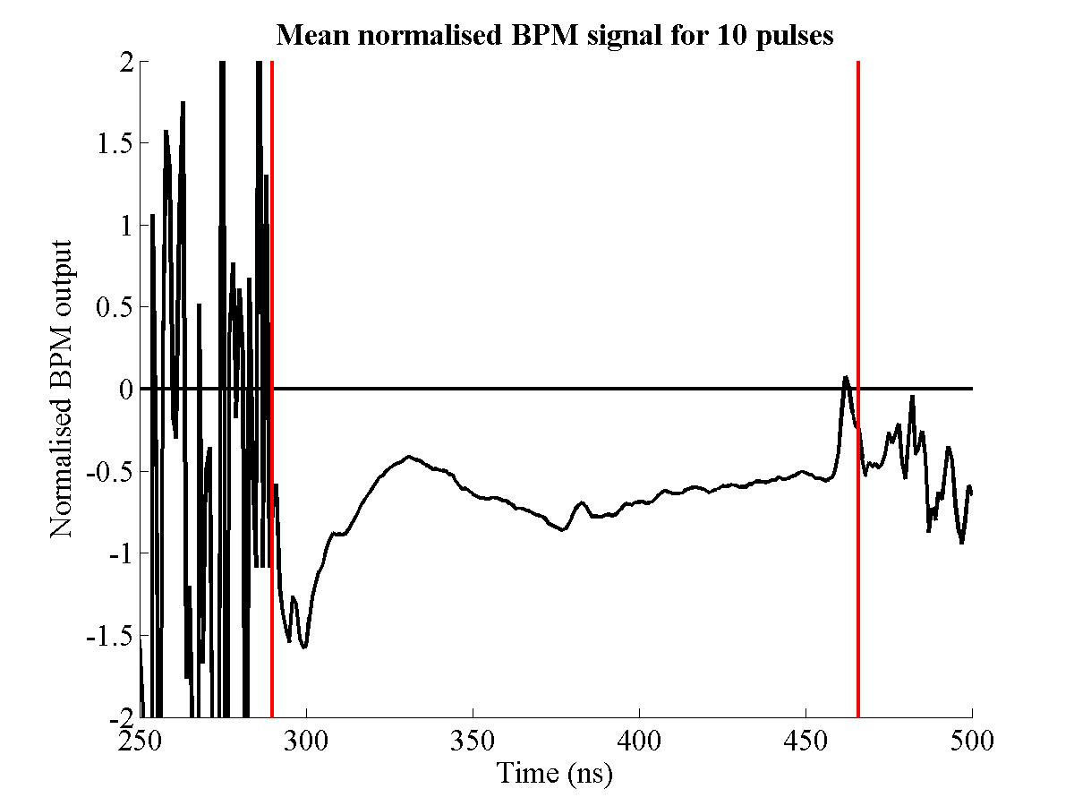
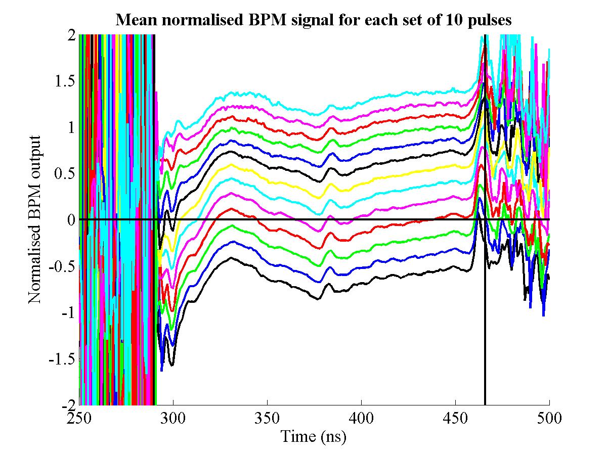
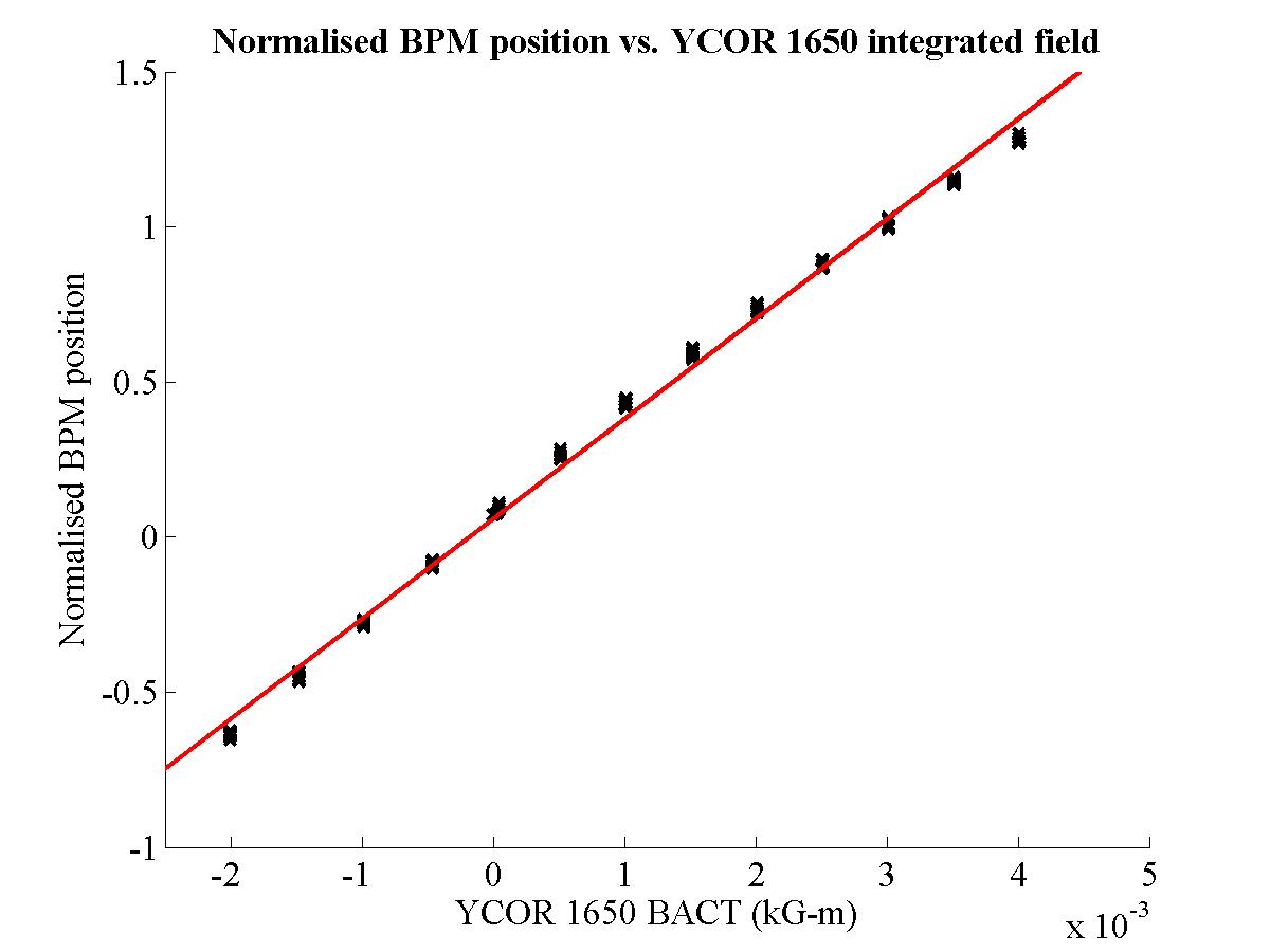
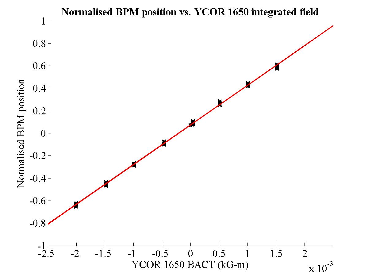
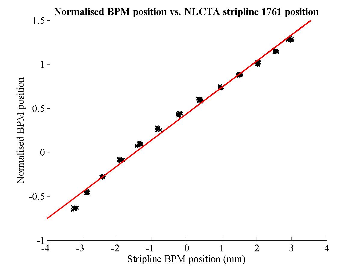
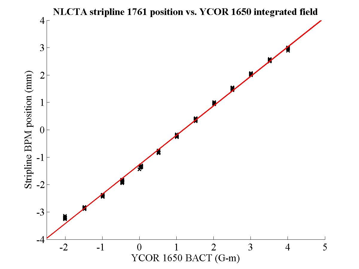
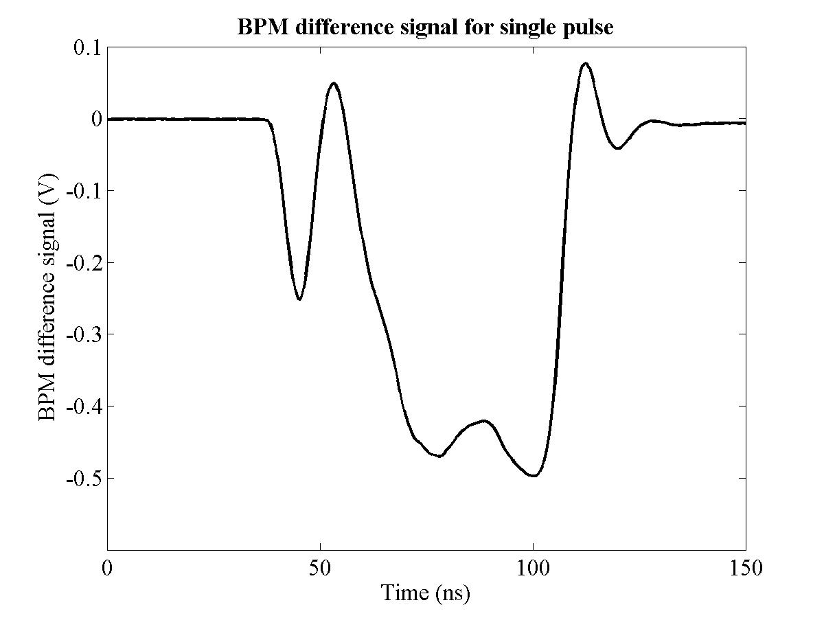
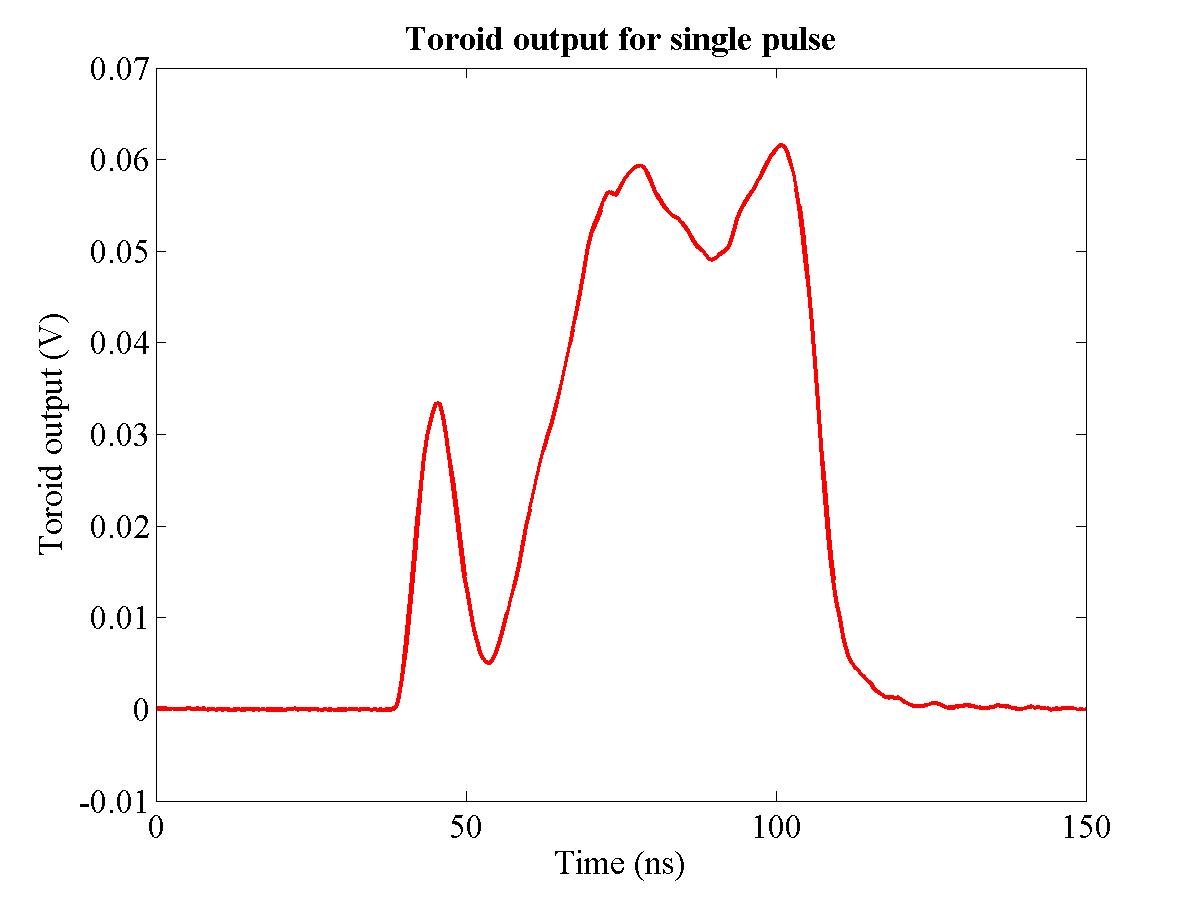
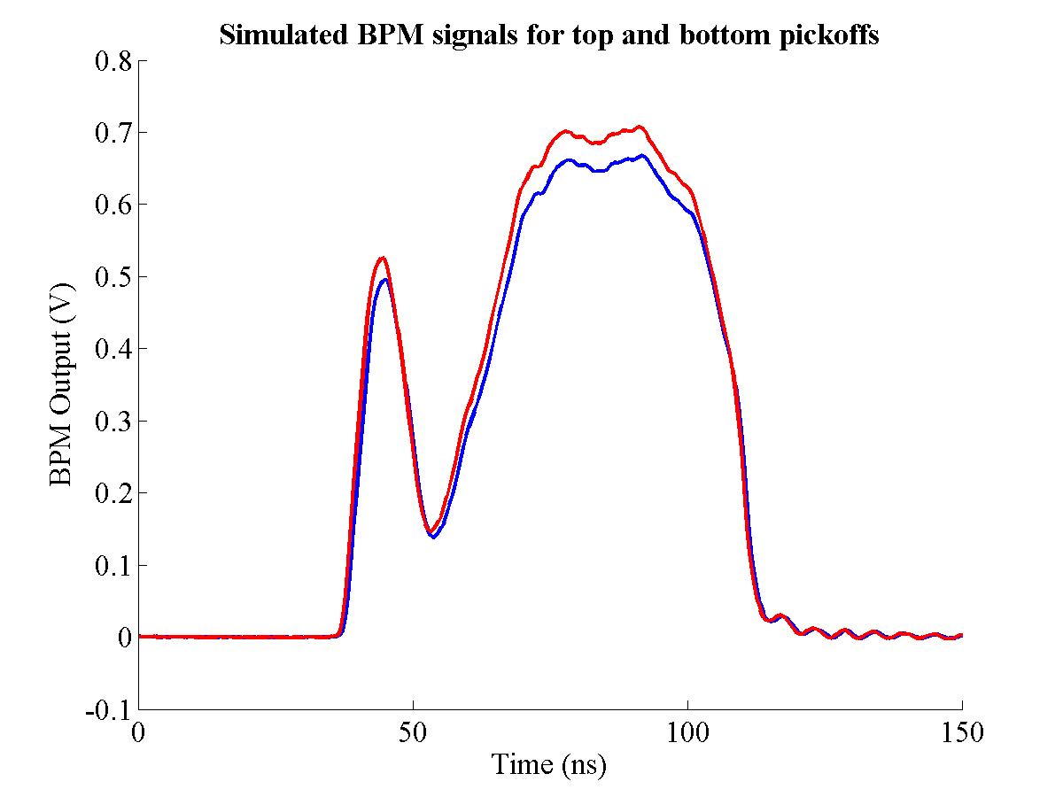
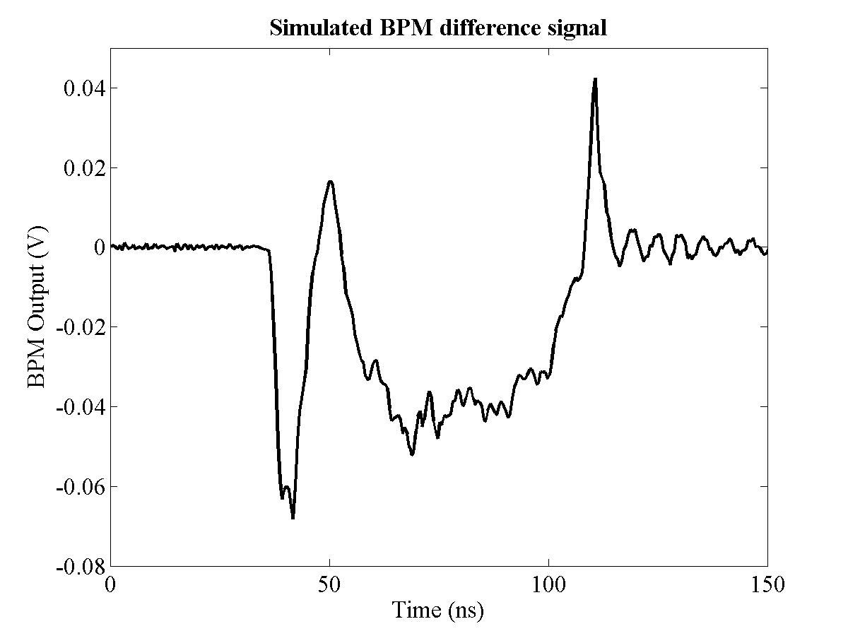
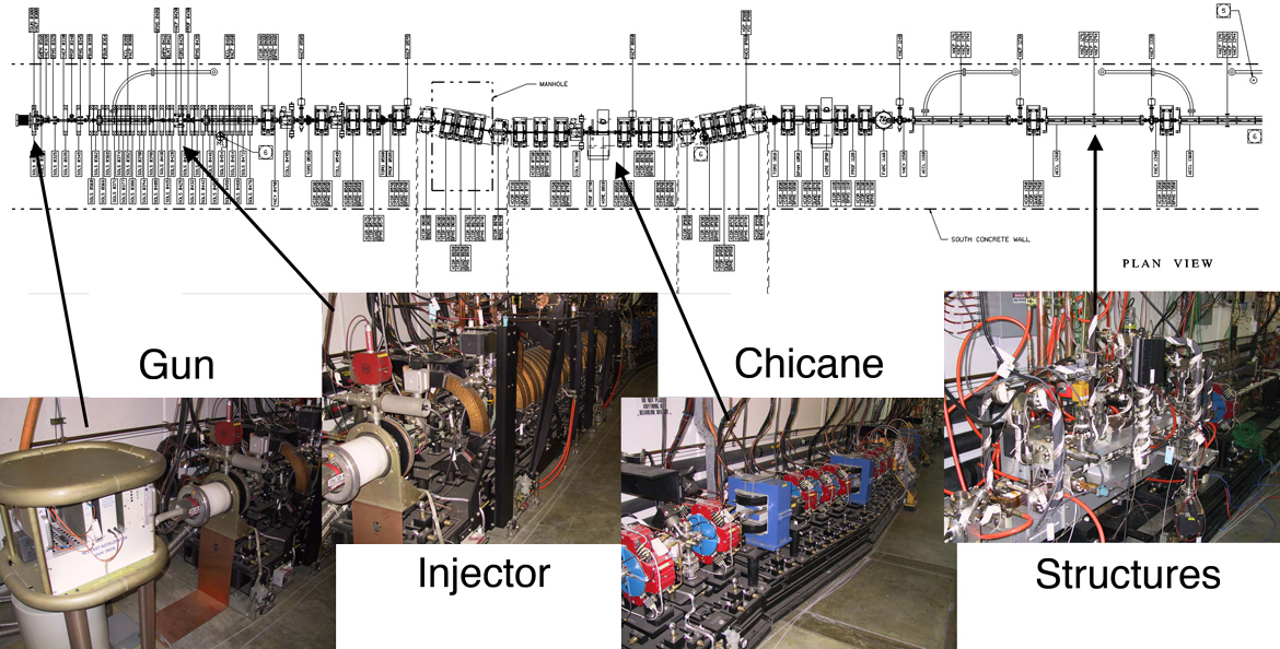
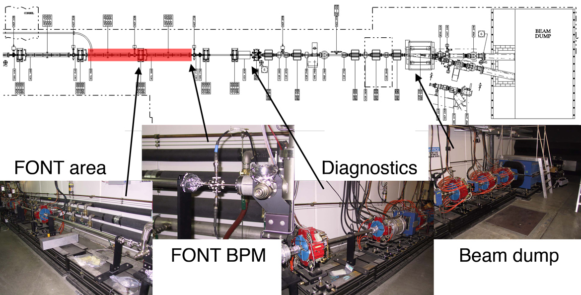
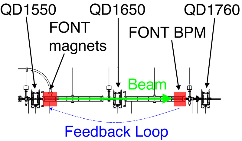
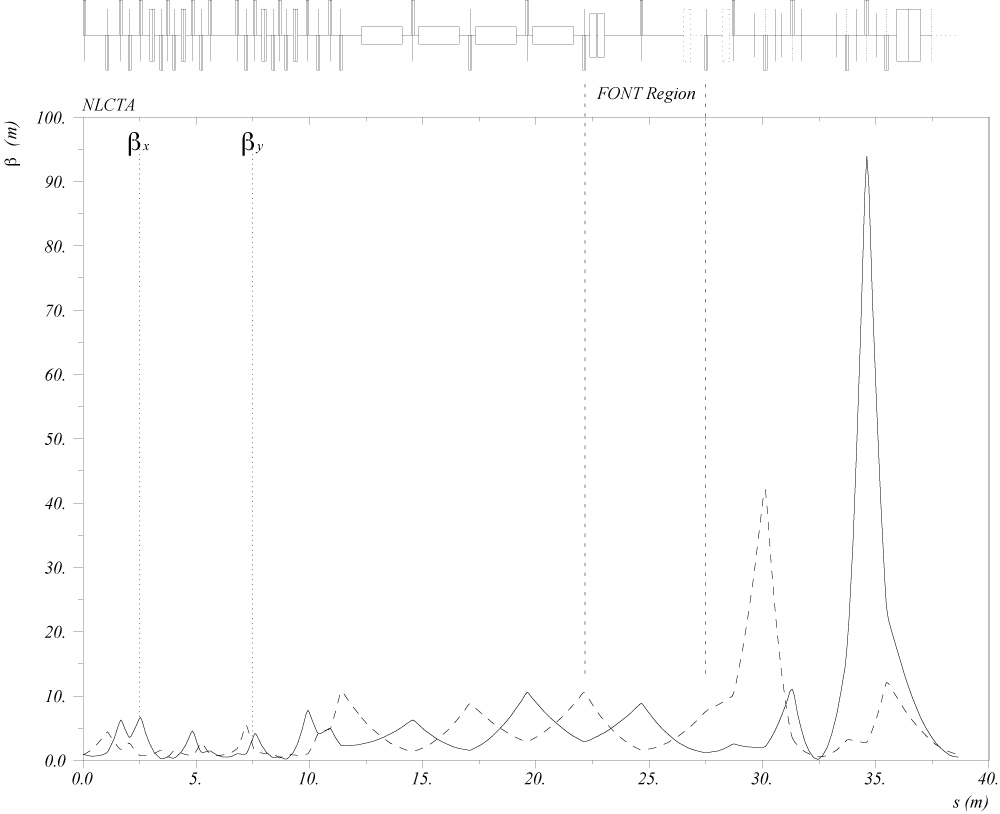
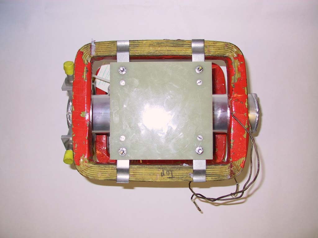
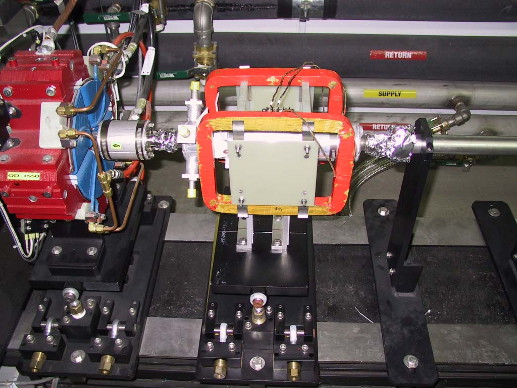
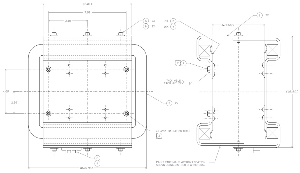
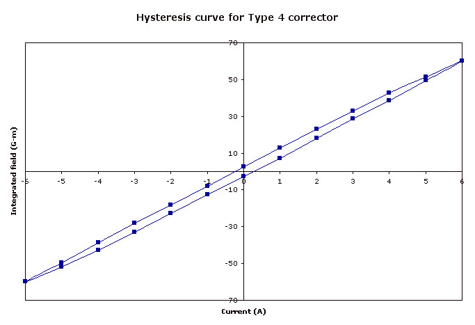
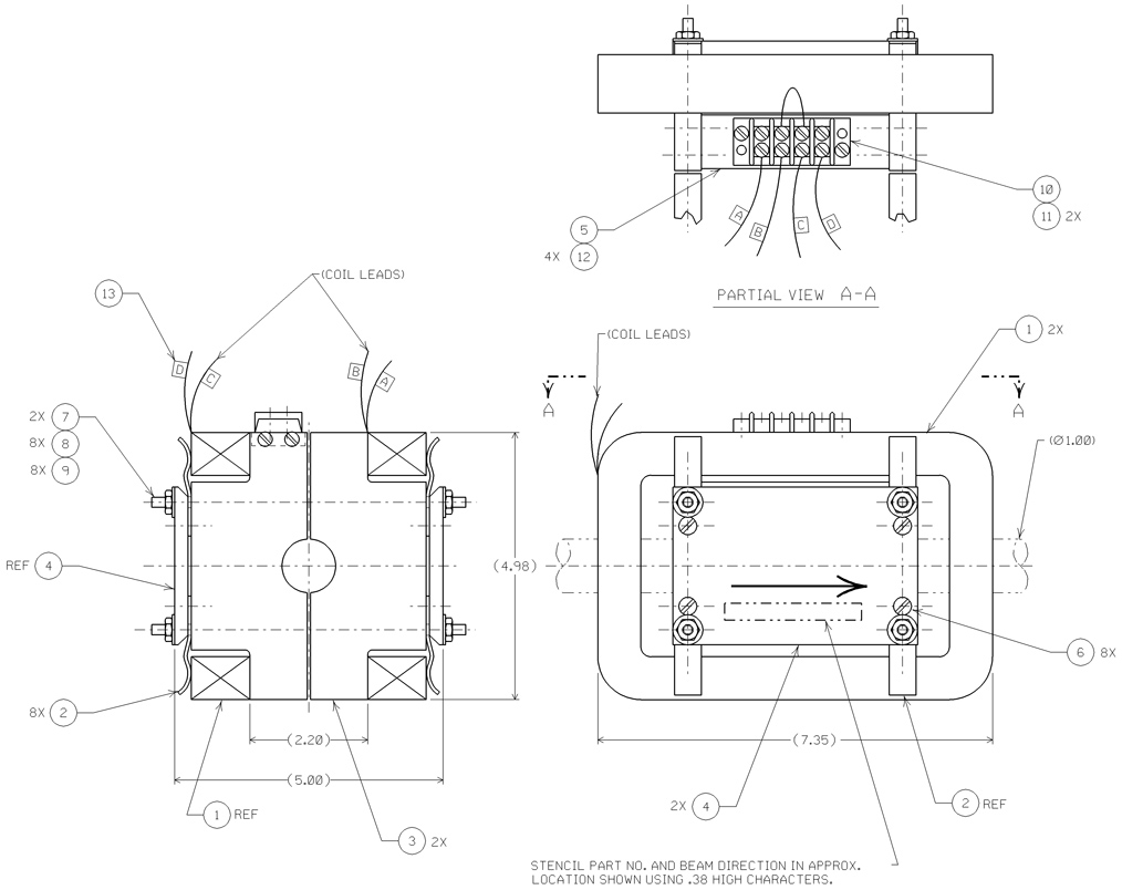
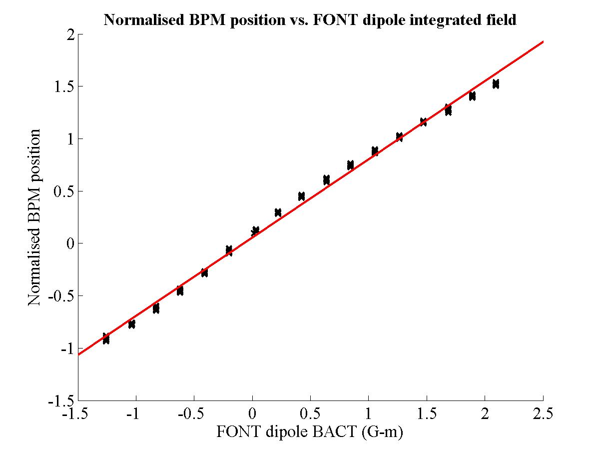
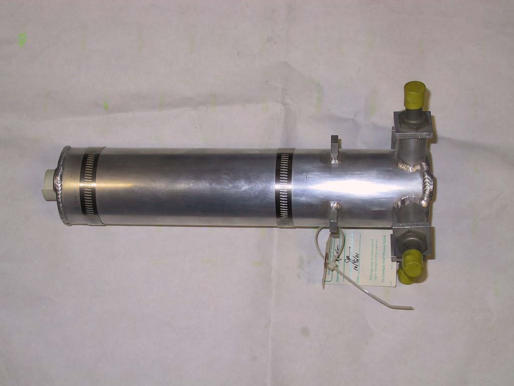
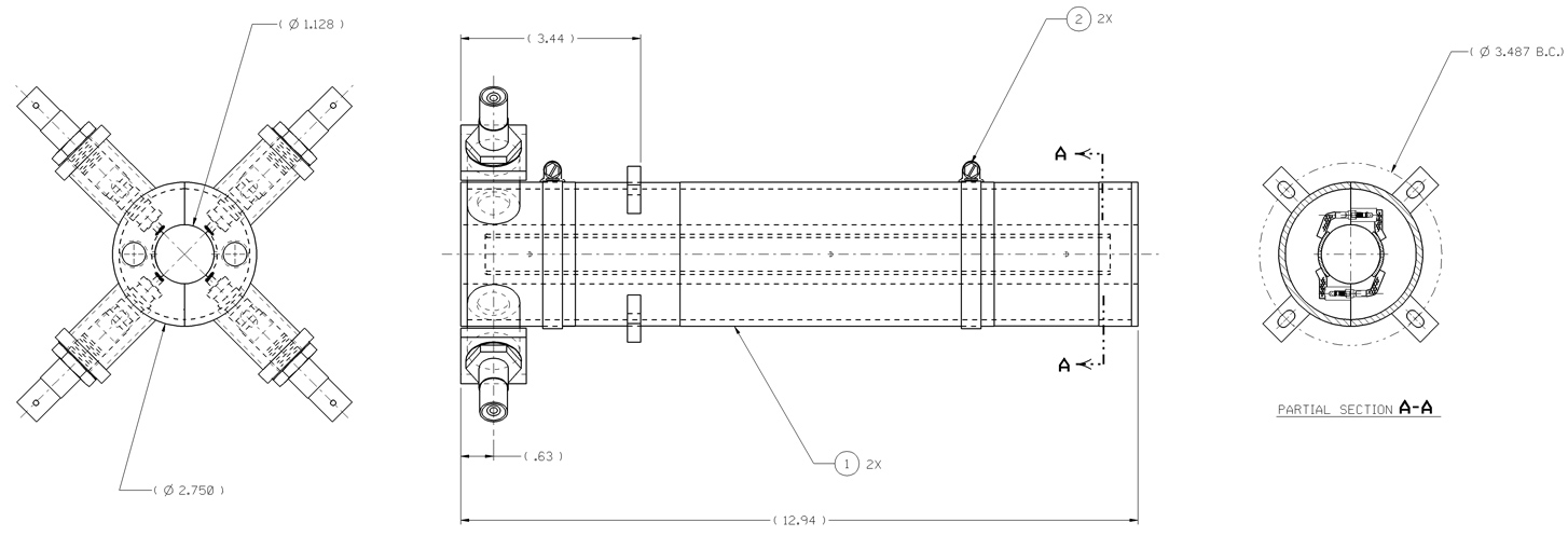
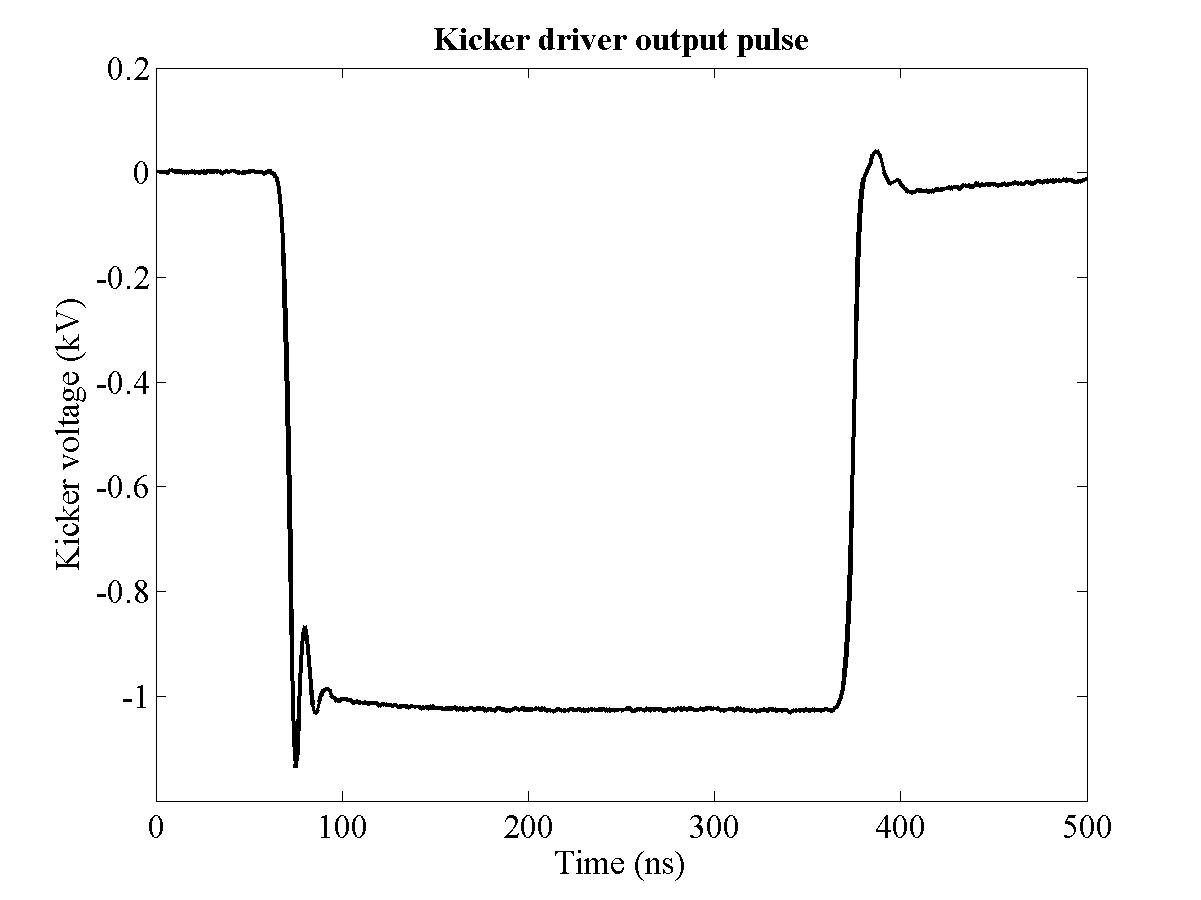
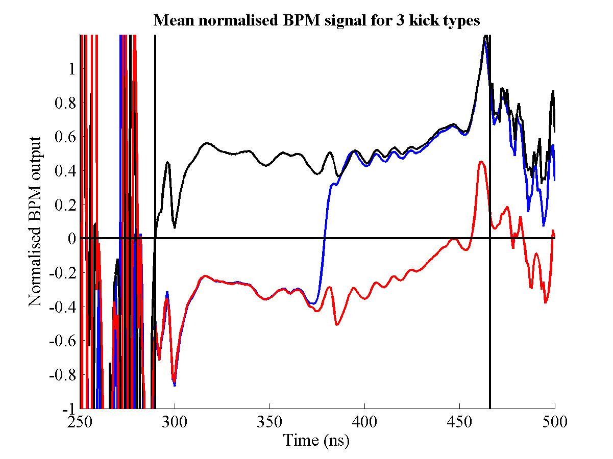
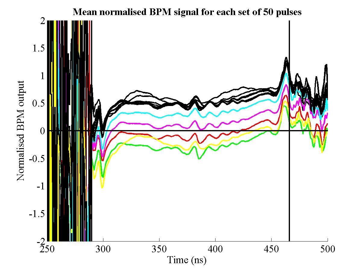
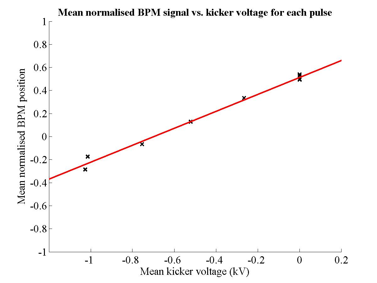
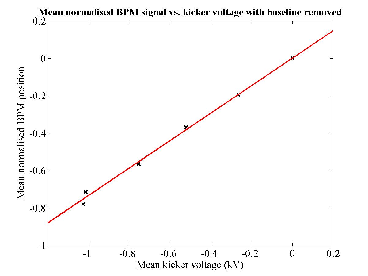
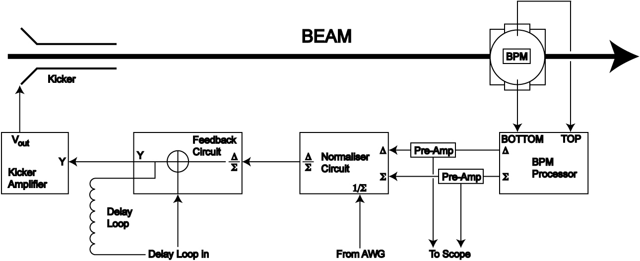
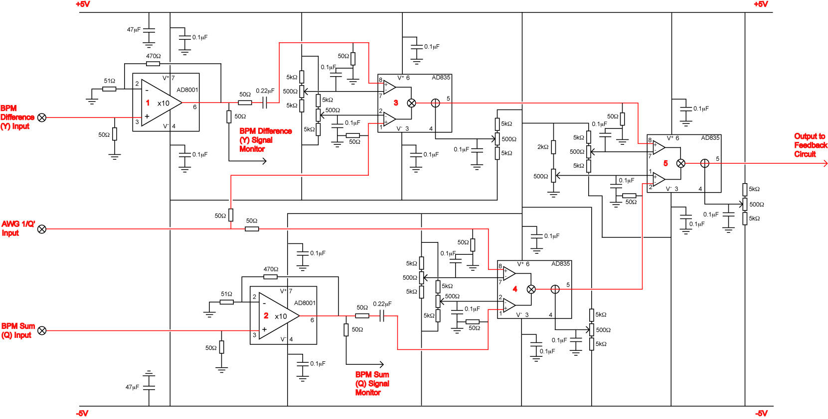
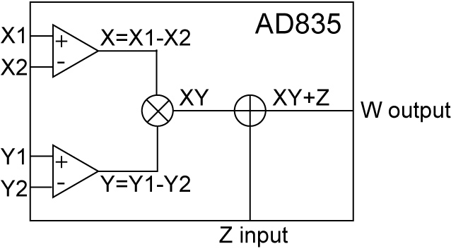
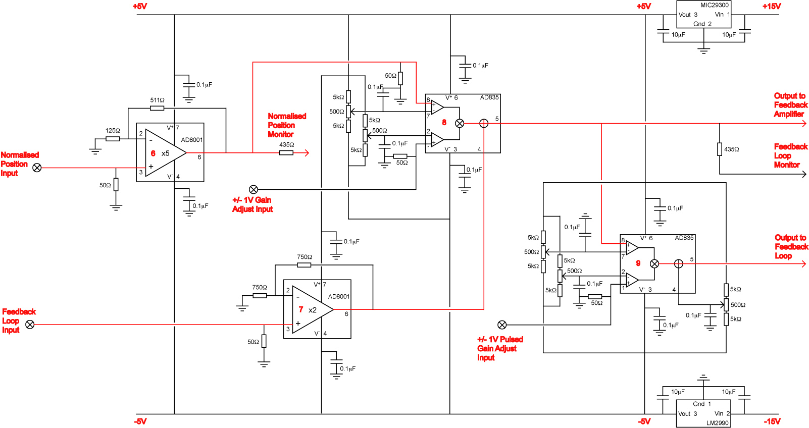
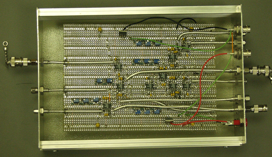
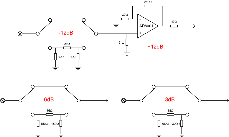
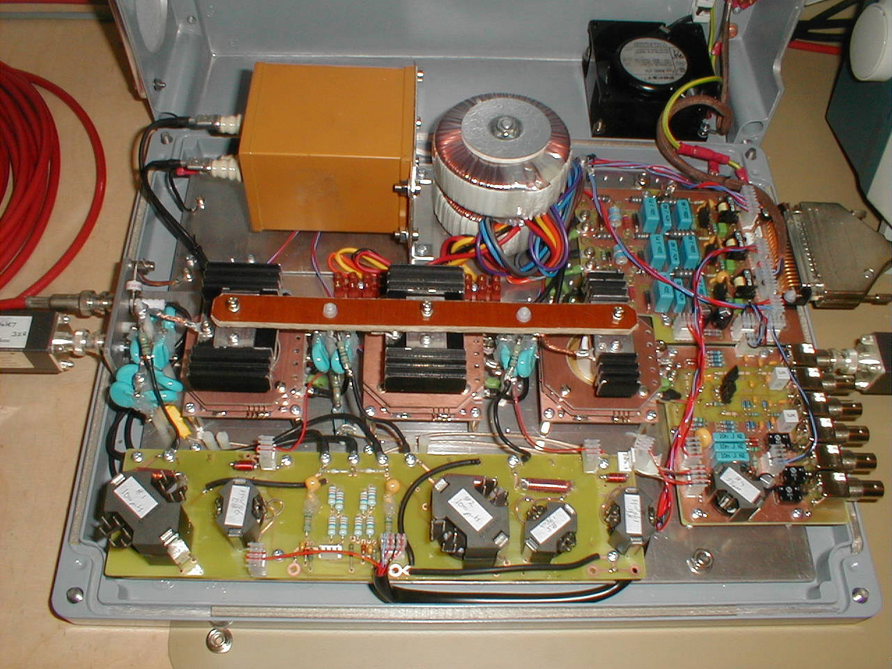
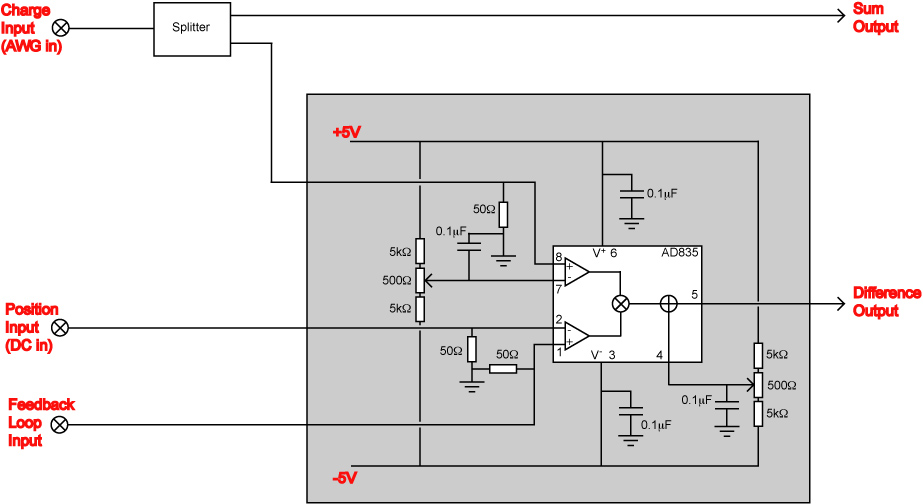
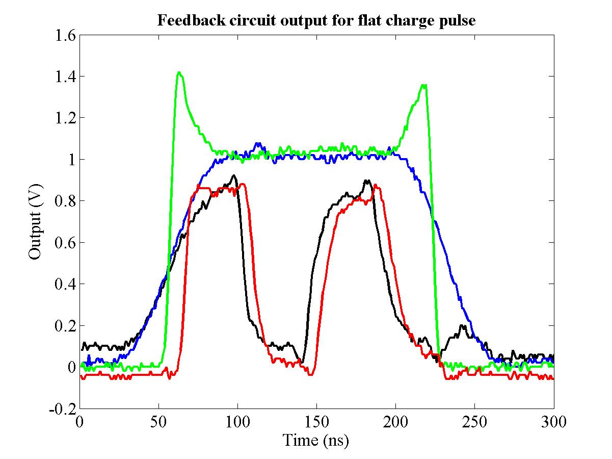
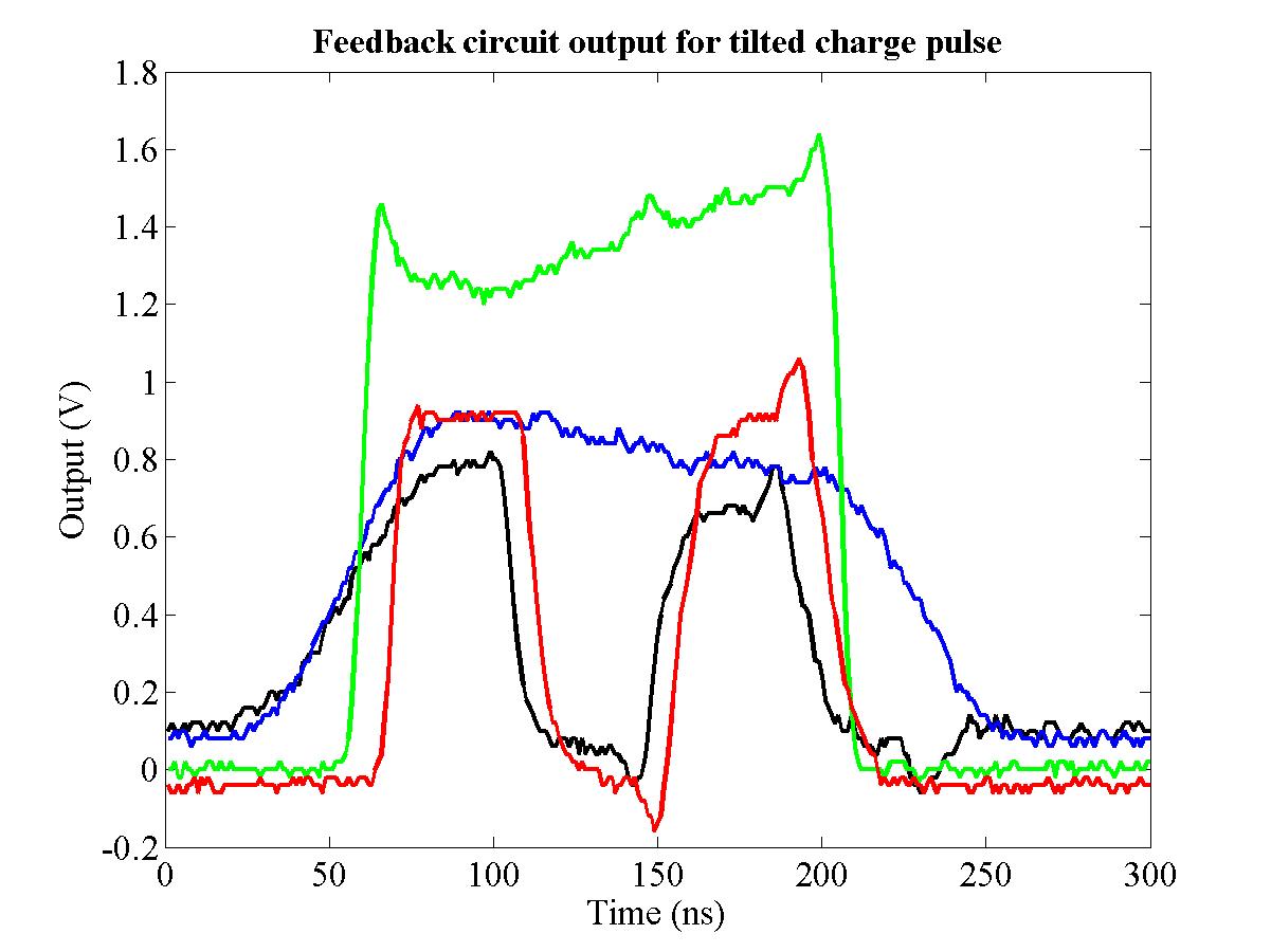
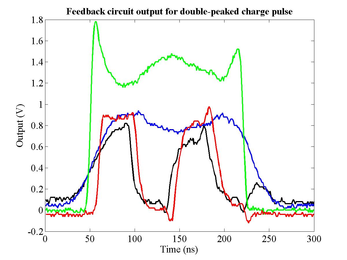
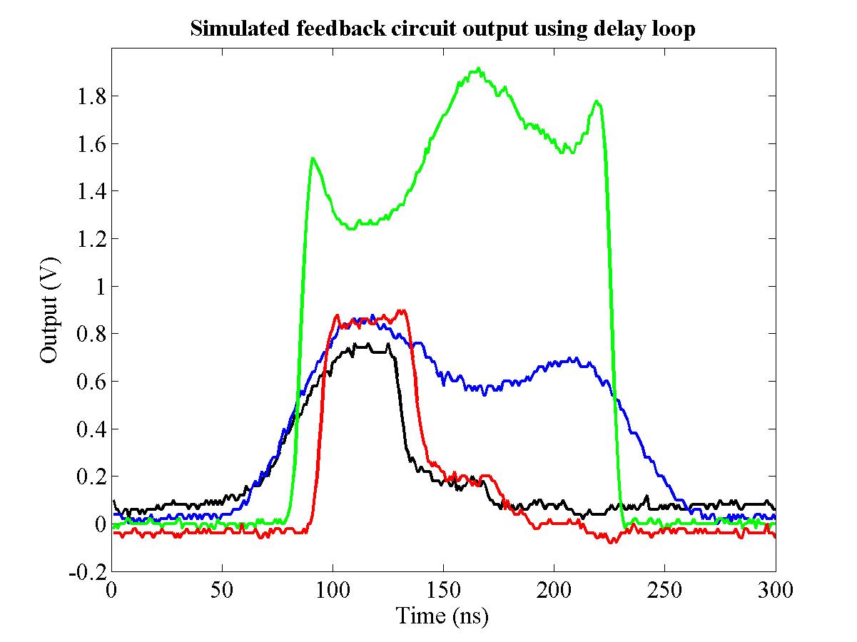
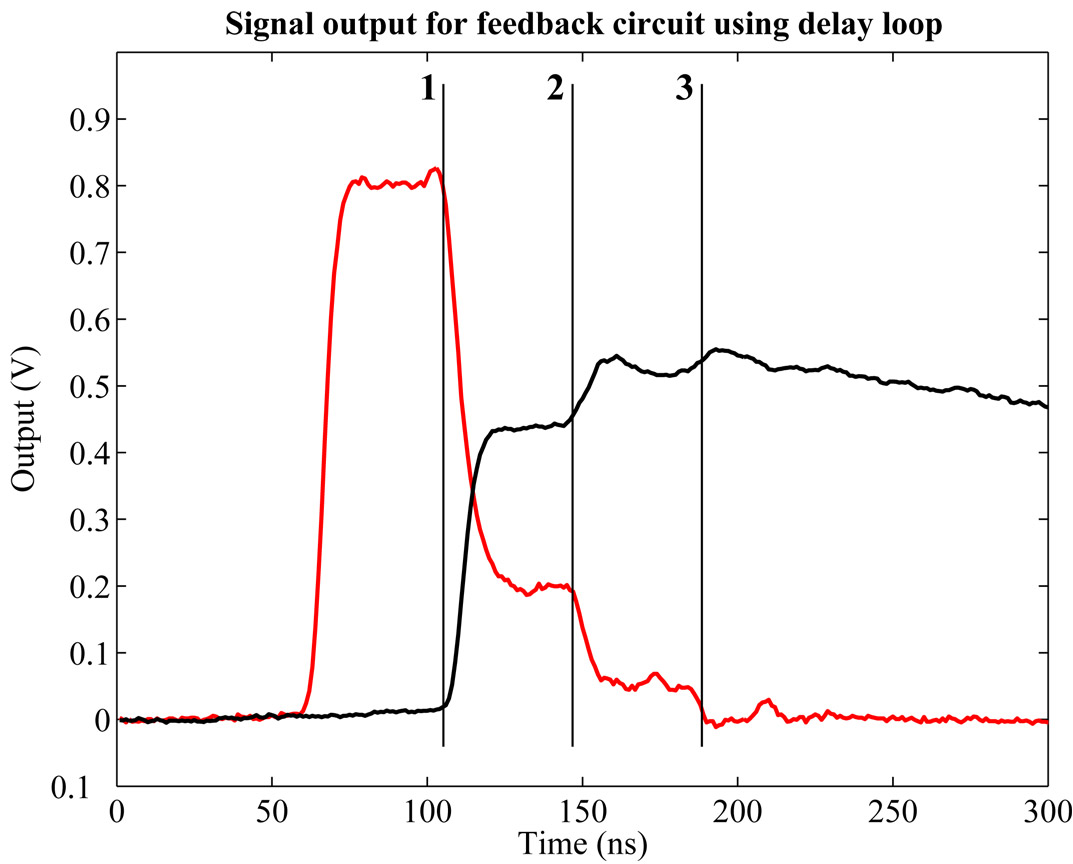
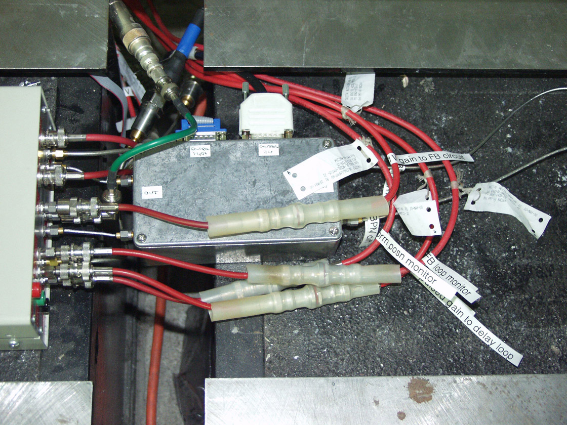
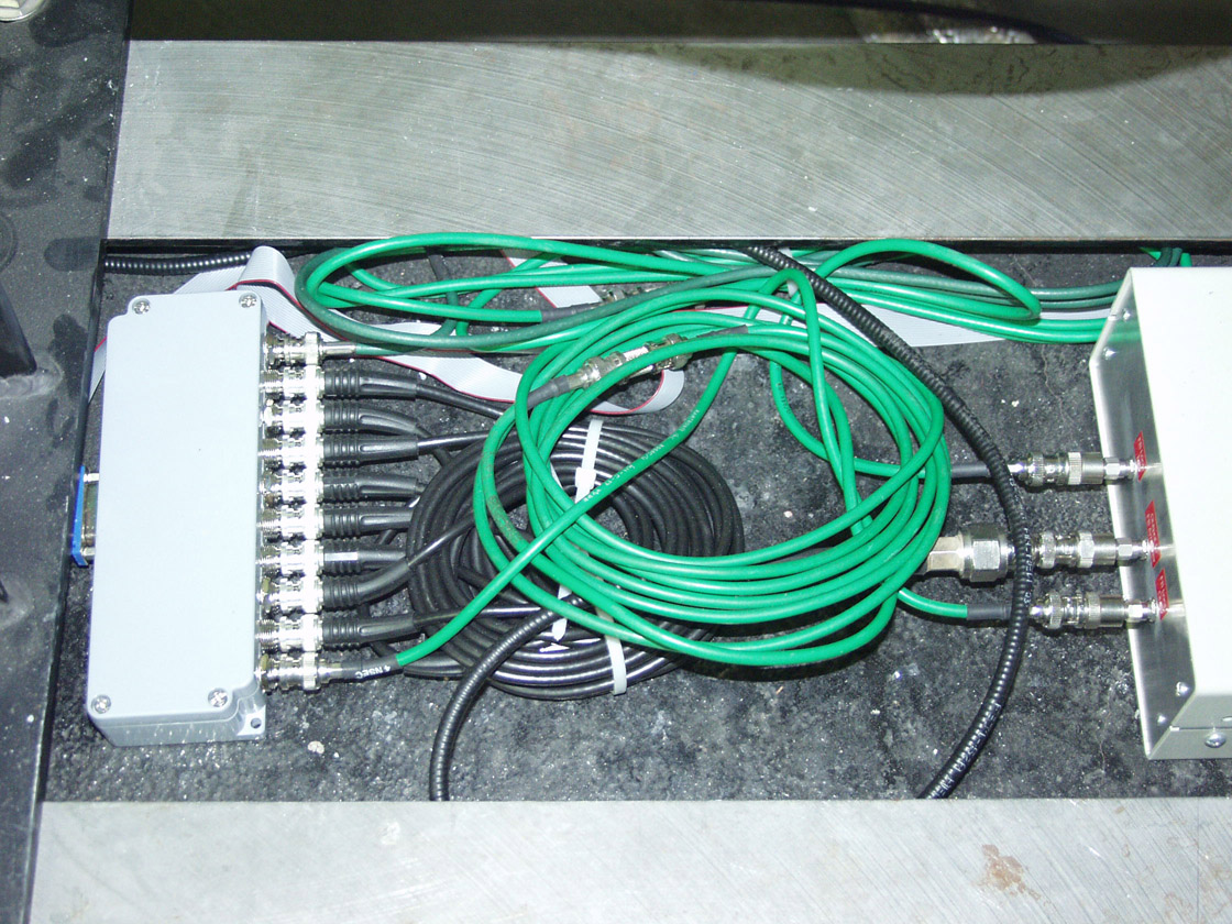
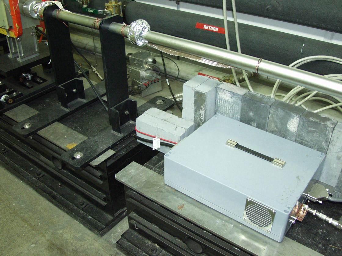
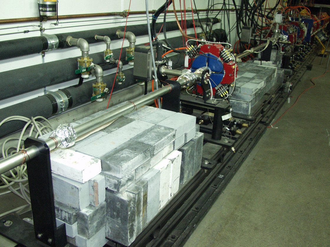
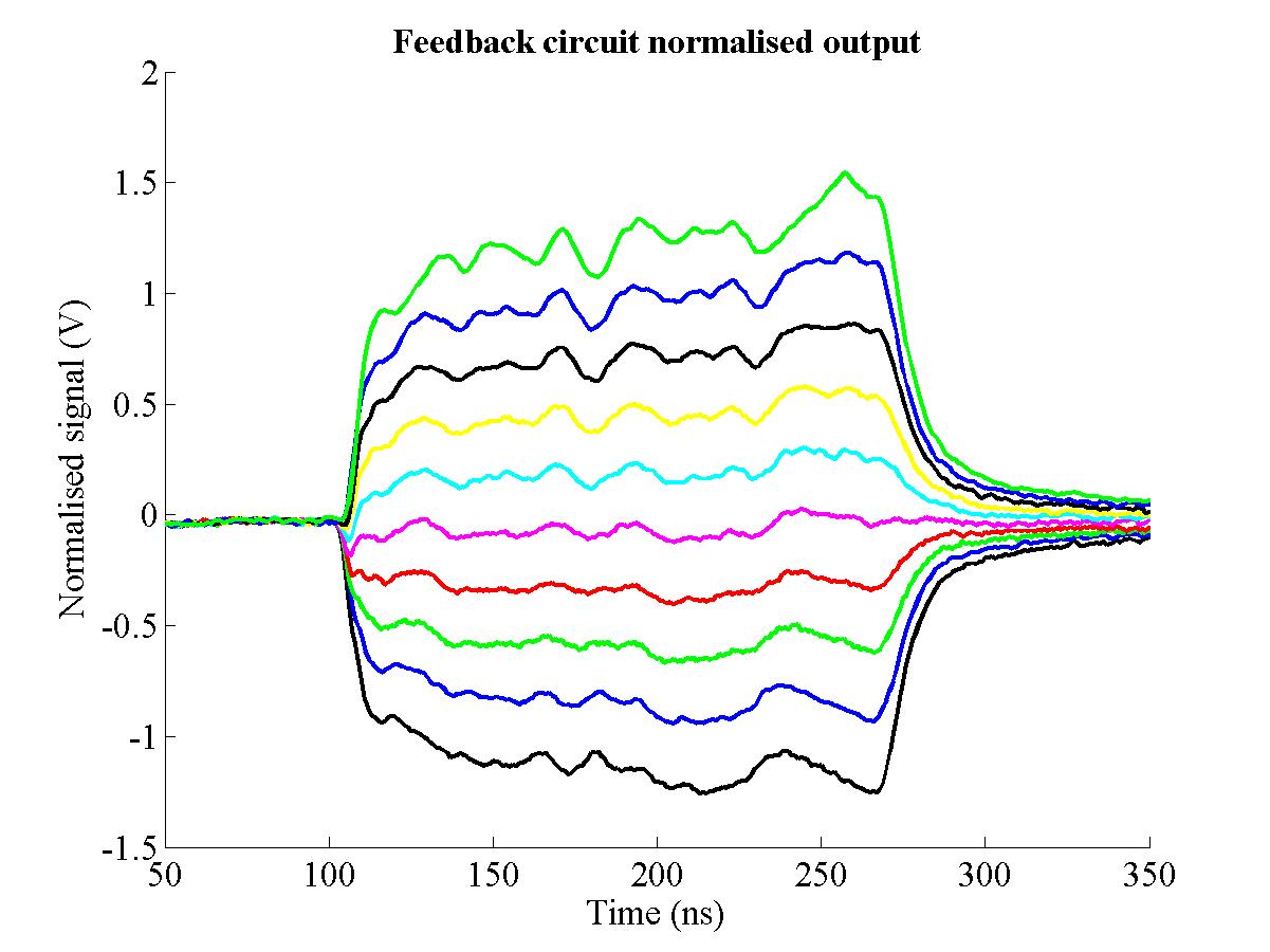
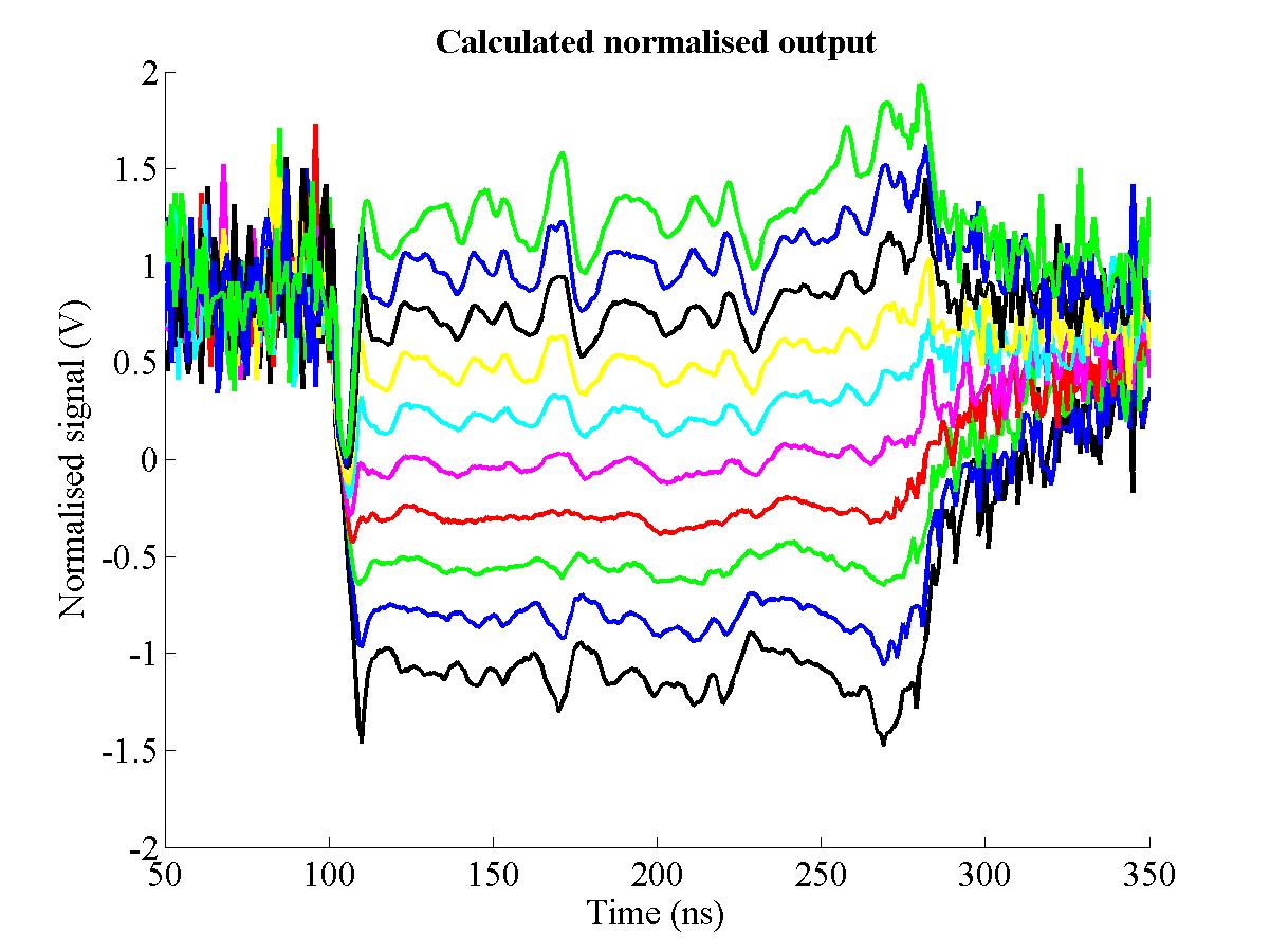
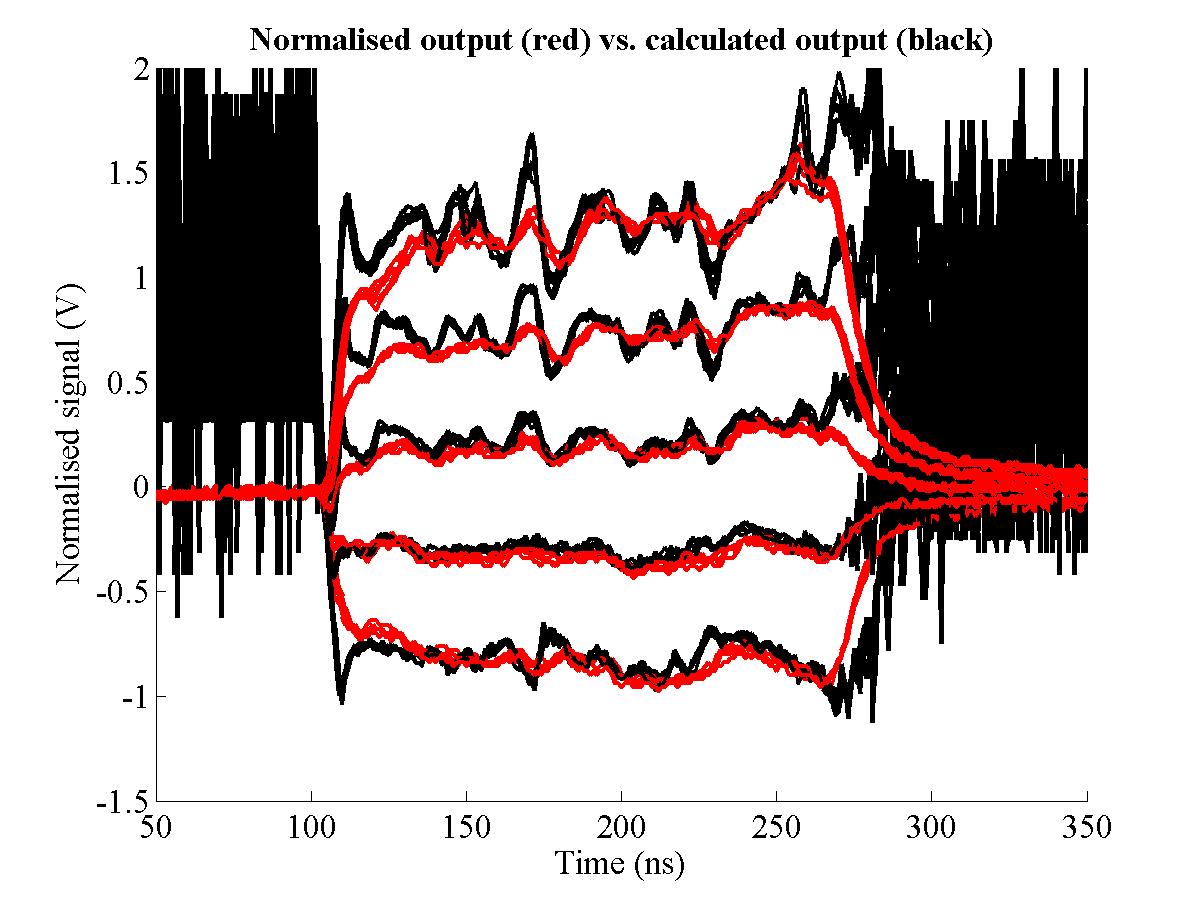
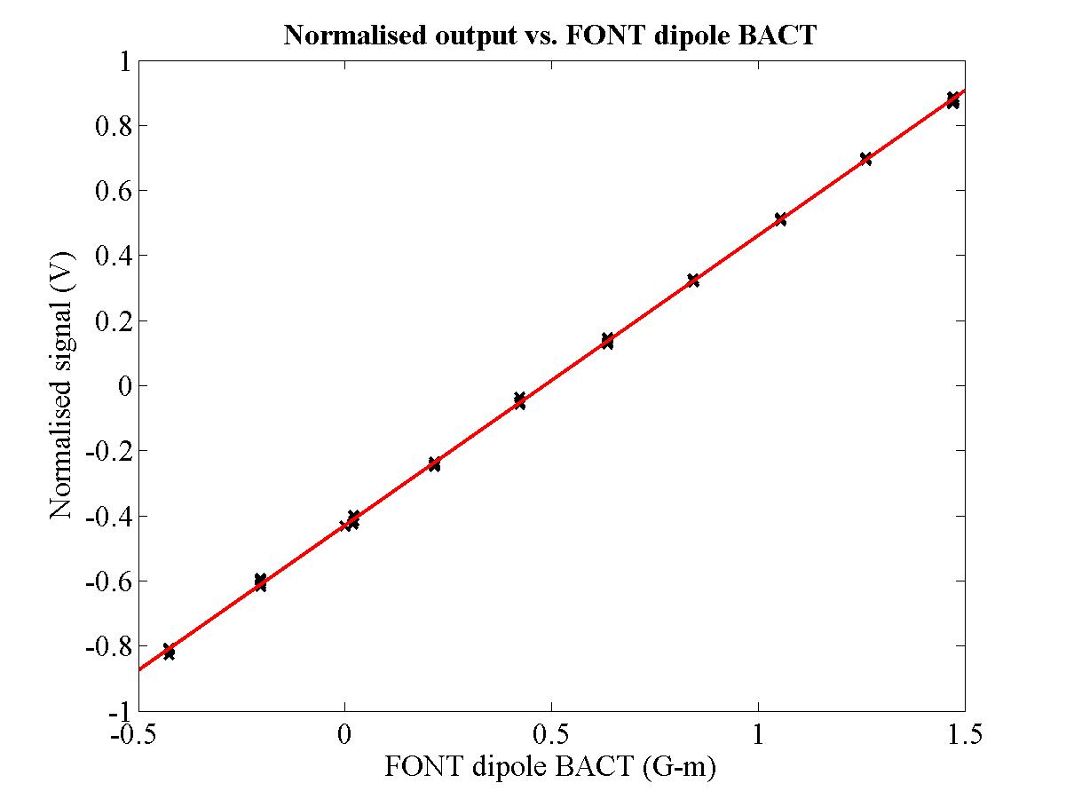
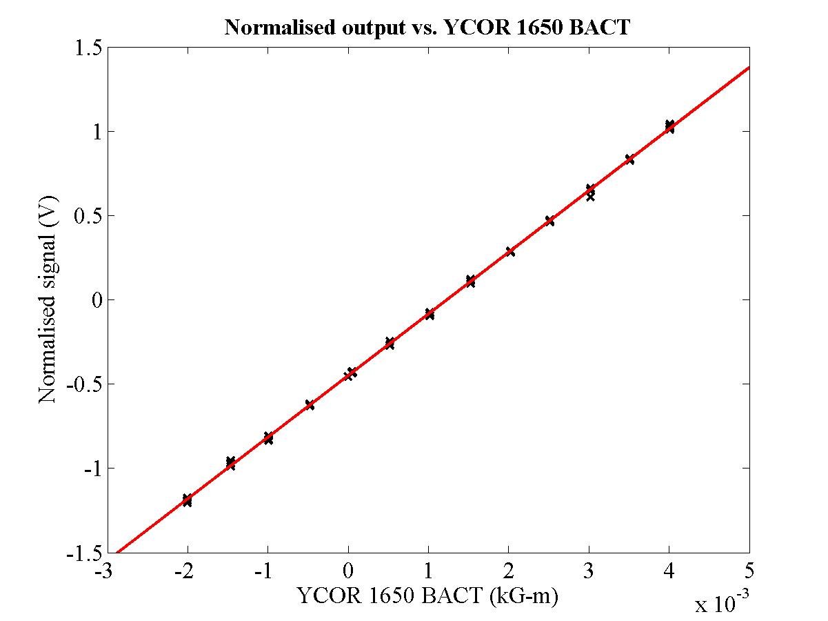
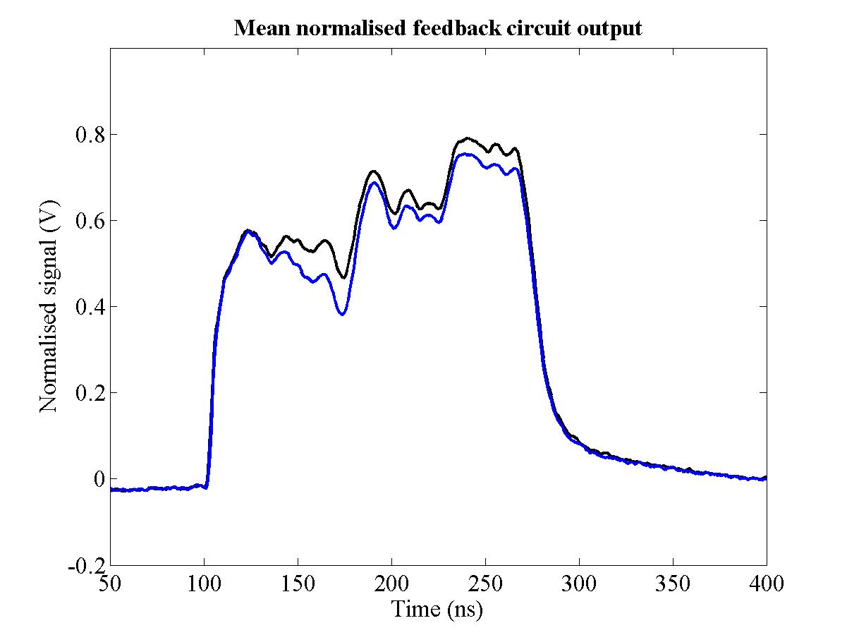
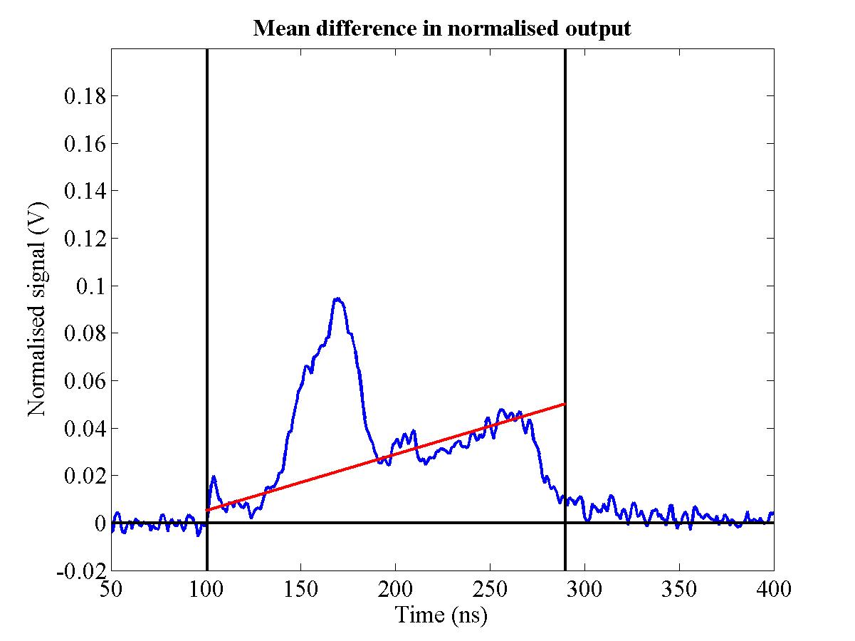
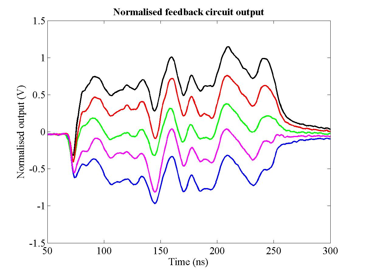
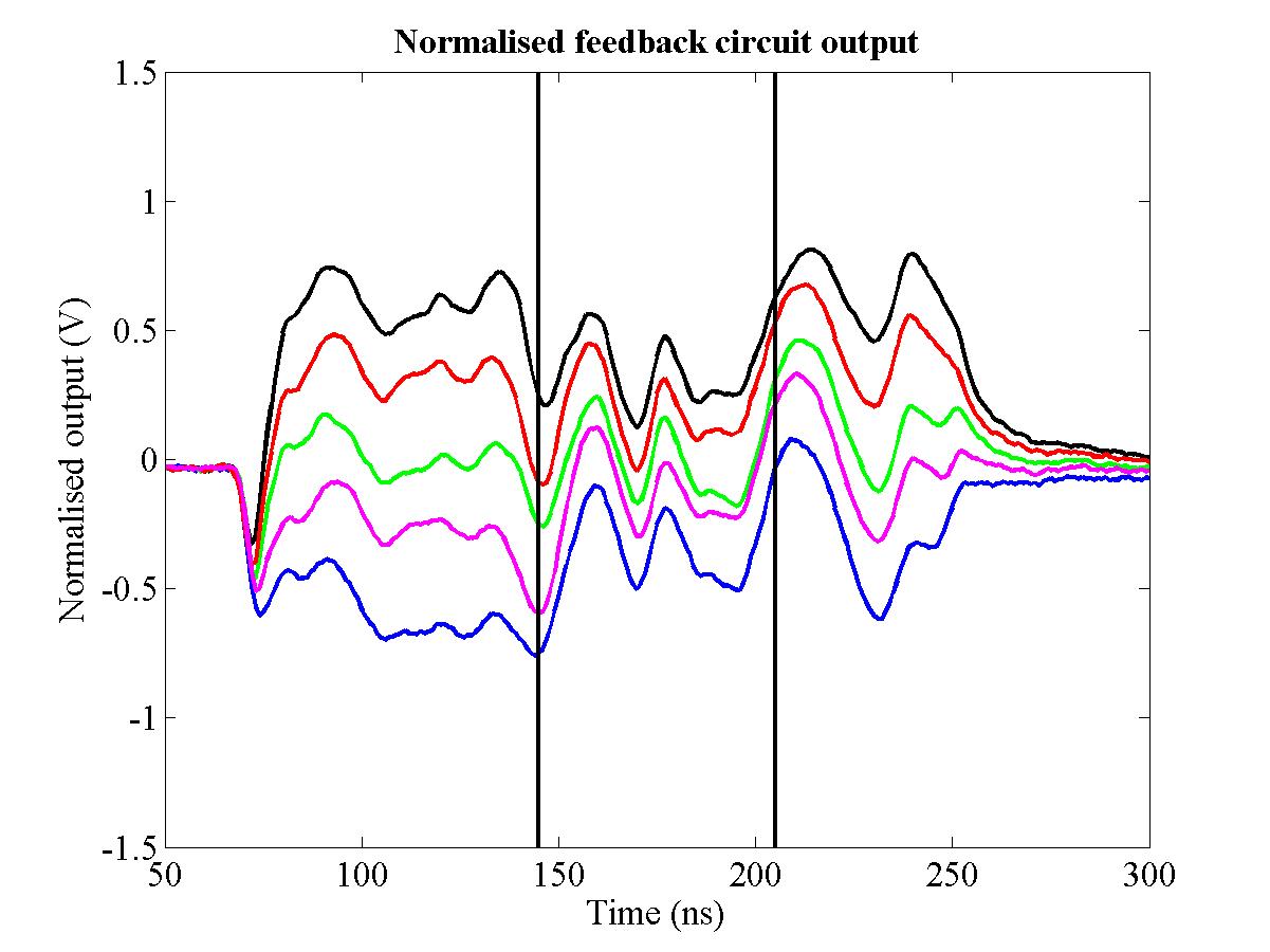
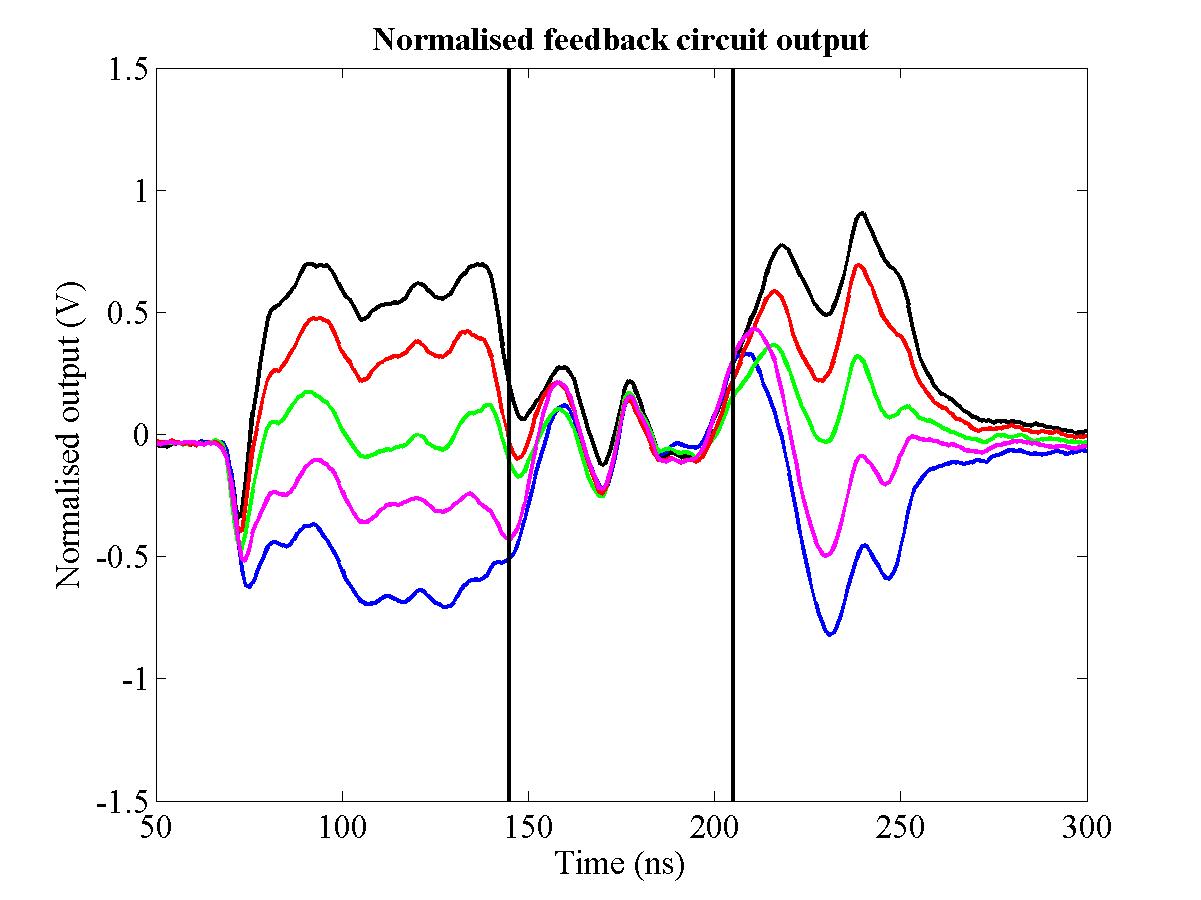
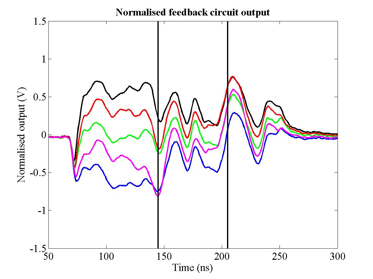
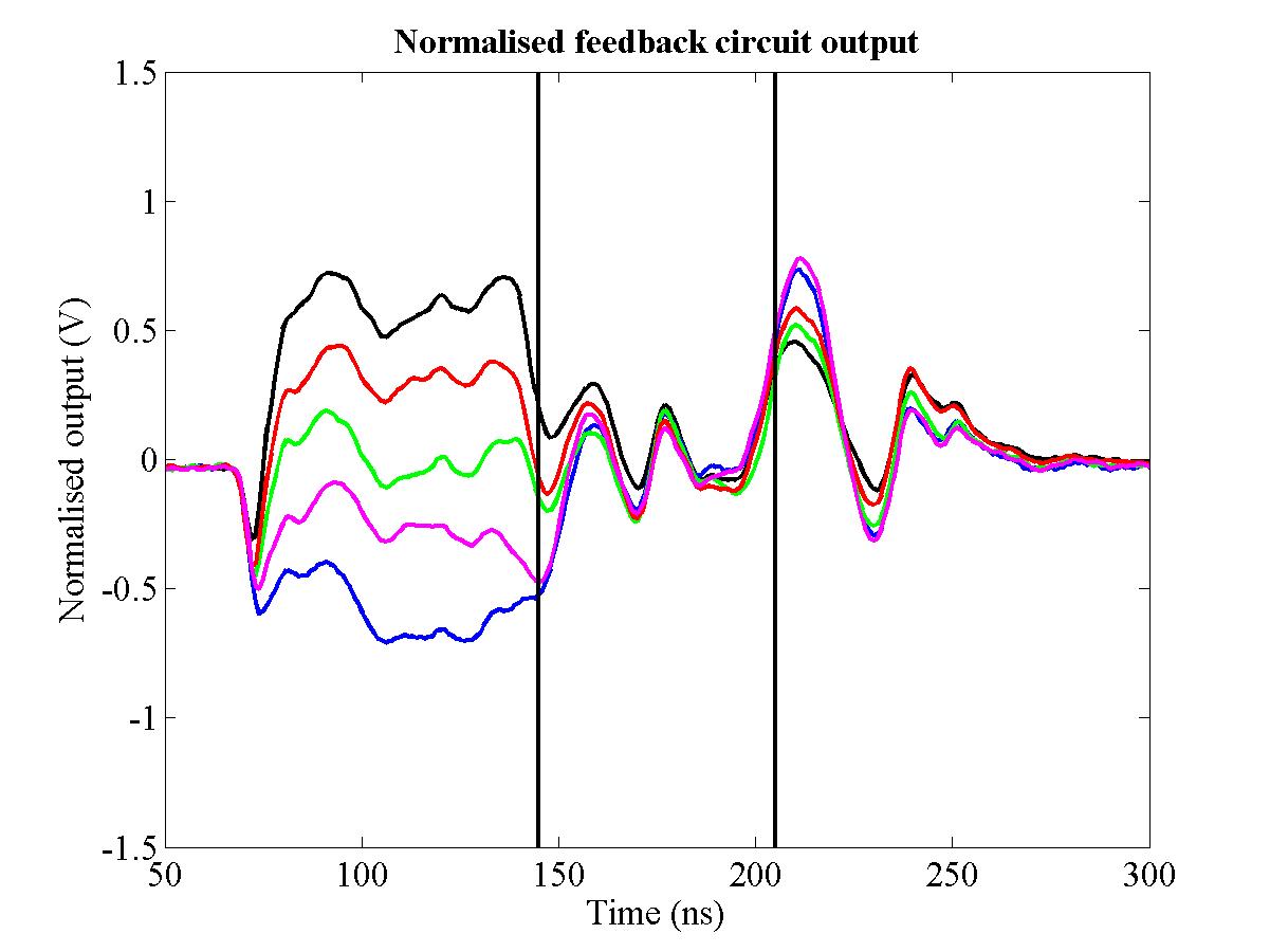
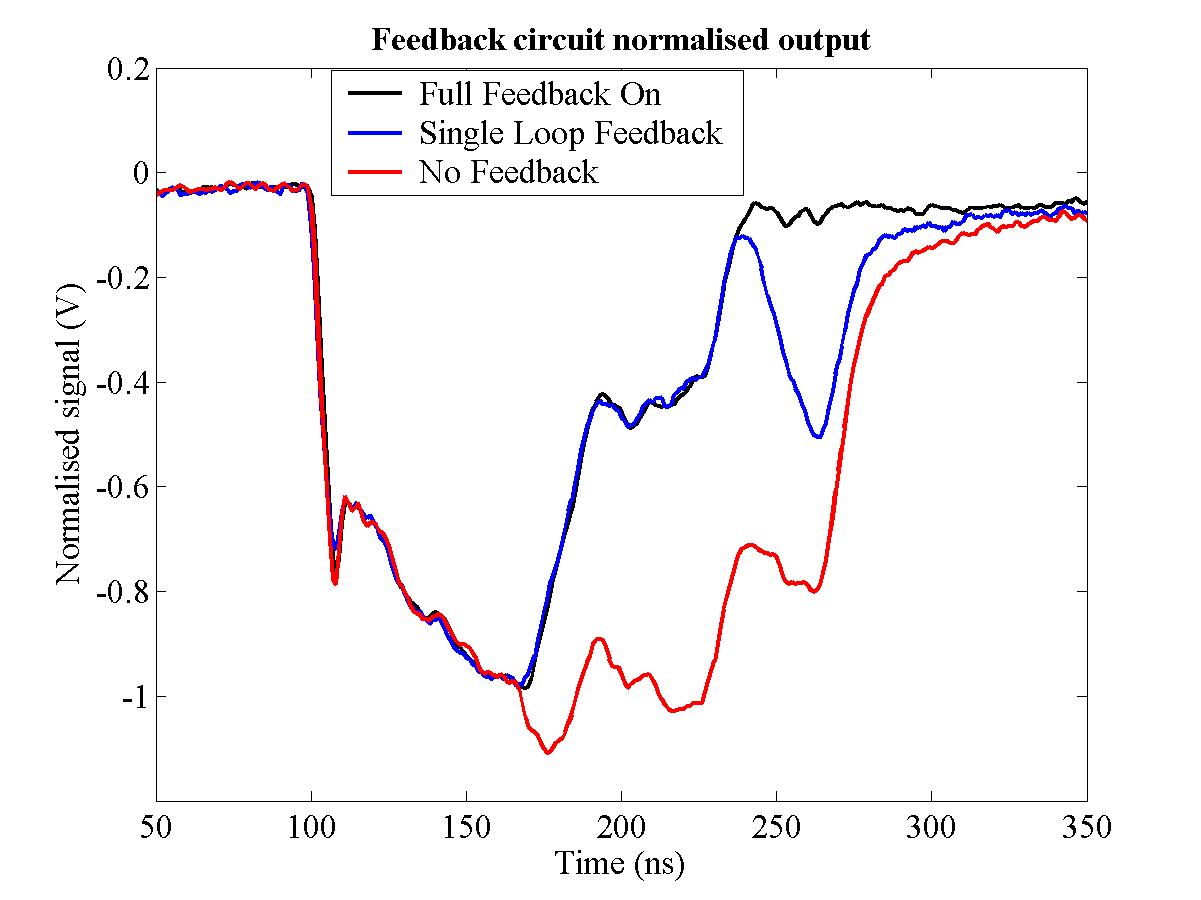