Proton Calorimetry/Experimental Runs/2021/Apr1: Difference between revisions
SaadShaikh (talk | contribs) No edit summary |
SaadShaikh (talk | contribs) No edit summary |
||
| Line 68: | Line 68: | ||
[http://www.hep.ucl.ac.uk/pbt/wikiData/images/DDC232/20210401/IMG_3575.JPG http://www.hep.ucl.ac.uk/pbt/wikiData/images/DDC232/20210401/IMG_3575.JPG]</div> | [http://www.hep.ucl.ac.uk/pbt/wikiData/images/DDC232/20210401/IMG_3575.JPG http://www.hep.ucl.ac.uk/pbt/wikiData/images/DDC232/20210401/IMG_3575.JPG]</div> | ||
|- | |- | ||
|15 || P, P, P, R || Yellow trace shows DVALID of first board at J2, blue shows 12V of first board at J2, purple shows DCLK of third board J3, green shows 12V of fourth board at J3. || <div class="image150px" style="text-align: center;"> [http://www.hep.ucl.ac.uk/pbt/wikiData/images/DDC232/20210401/IMG_3576.JPG http://www.hep.ucl.ac.uk/pbt/wikiData/images/DDC232/20210401/IMG_3576.JPG]</div> <div class="image150px" style="text-align: center;"> [http://www.hep.ucl.ac.uk/pbt/wikiData/images/DDC232/20210401/IMG_3577.JPG http://www.hep.ucl.ac.uk/pbt/wikiData/images/DDC232/20210401/IMG_3577.JPG]</div> | |15 || P, P, P, R || Yellow trace shows DVALID of first board at J2, blue shows 12V of first board at J2, purple shows DCLK of third board J3, green shows 12V of fourth board at J3. Second image has yellow and purple showing DCLK of different boards (unsure which ones). || <div class="image150px" style="text-align: center;"> [http://www.hep.ucl.ac.uk/pbt/wikiData/images/DDC232/20210401/IMG_3576.JPG http://www.hep.ucl.ac.uk/pbt/wikiData/images/DDC232/20210401/IMG_3576.JPG]</div> <div class="image150px" style="text-align: center;"> [http://www.hep.ucl.ac.uk/pbt/wikiData/images/DDC232/20210401/IMG_3577.JPG http://www.hep.ucl.ac.uk/pbt/wikiData/images/DDC232/20210401/IMG_3577.JPG]</div> | ||
|- | |- | ||
|16 || N/A || Yellow shows CLK pin directly from FPGA without any board connected. || <div class="image150px" style="text-align: center;"> | |16 || N/A || Yellow shows CLK pin directly from FPGA without any board connected. || <div class="image150px" style="text-align: center;"> | ||
Latest revision as of 12:28, 7 April 2021
Daisy chain tests of second DDC232 prototype in D109
Aim: Debug "mirroring" issues when daisy-chaining more than 2 DDC232s boards. Test signal quality across boards using 500MHz oscilloscope.
Notes
- 3 DDC232 boards have S12915-16R photodiodes.
- 1 DDC232 board has 1k ohm resistors.
- In the runs below, boards are enumerated right to left, with the right-most board (1st board) connected to the FPGA.
- In the configuration column, P = board with photodiodes and R = board with resistors. The first board listed in this column is connected to the FPGA.
- In all runs, an integration time of 170us and full-scale range of 350pC is used.
Traces saved in /unix/www/html/pbt/wikiData/images/DDC232/20210401
| Run | Board Configuration | Scope Trace Description | Oscilloscope Trace |
|---|---|---|---|
| 1 | P | Yellow trace shows DVALID at FPGA, blue shows DVALID at J2 of DDC232 board. | 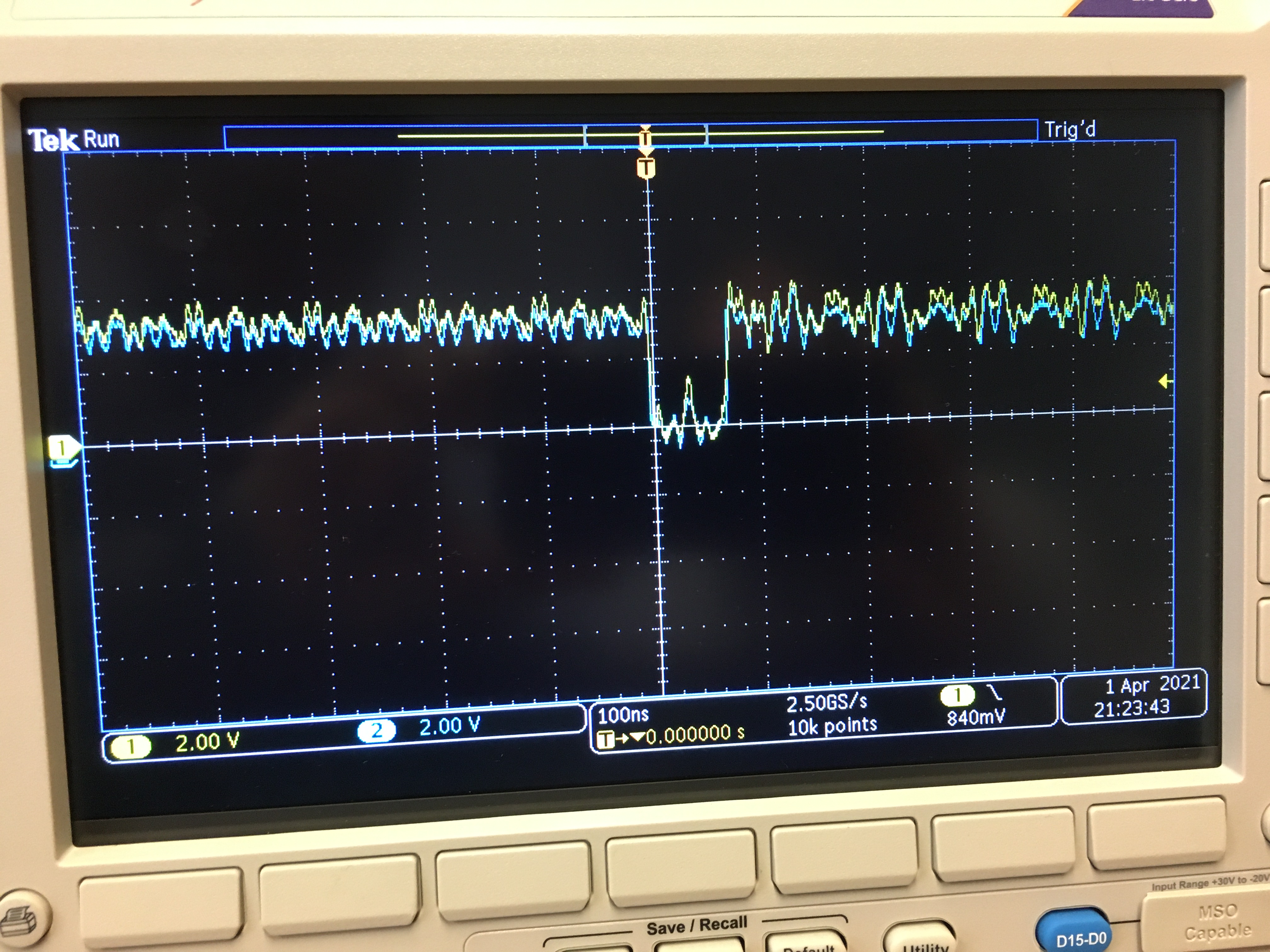 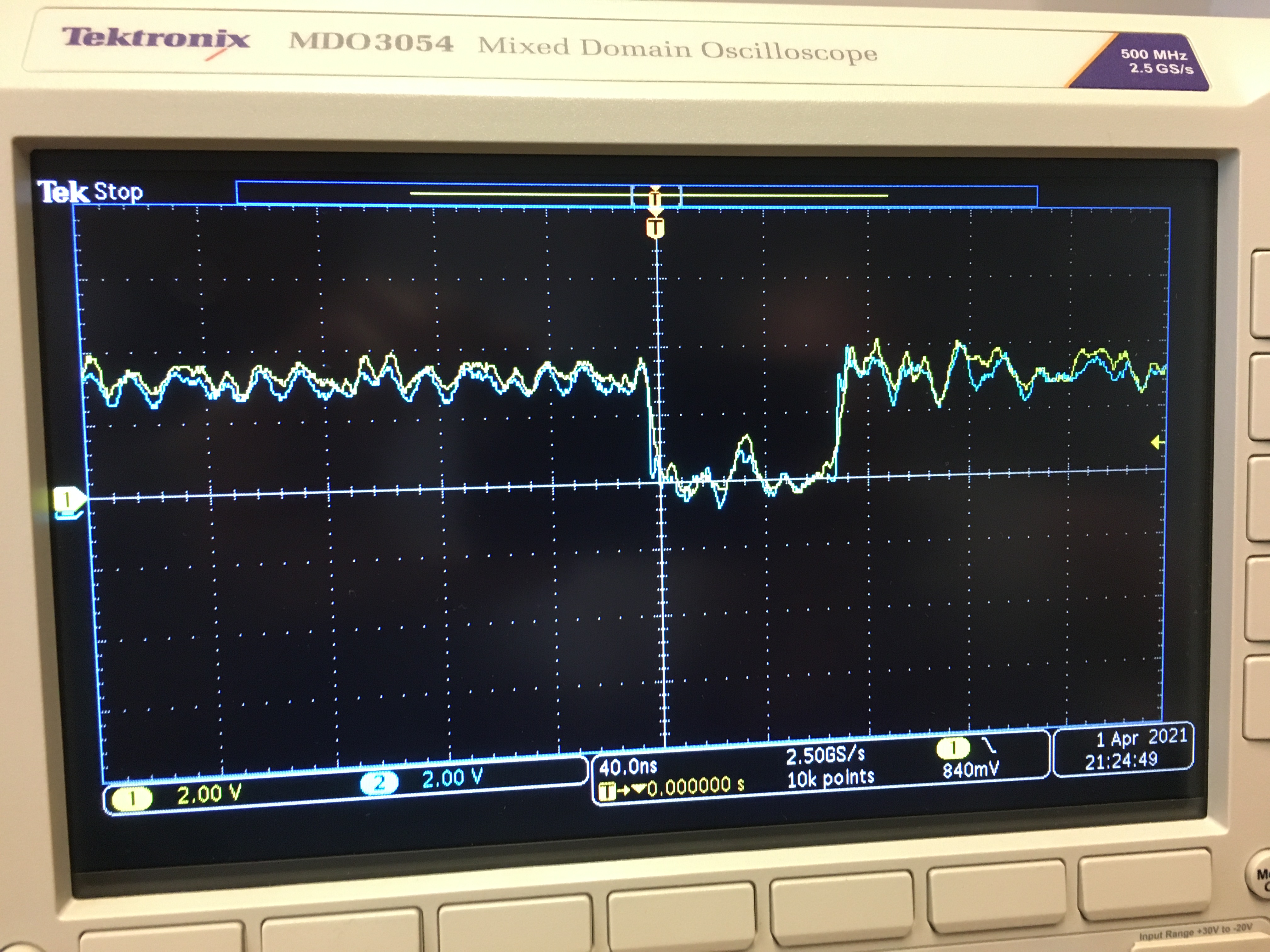 |
| 2 | P | Yellow trace shows DVALID at FPGA, green shows CLK at J2 of DDC232 board, purple shows 12V at J2 of DDC232 board. | 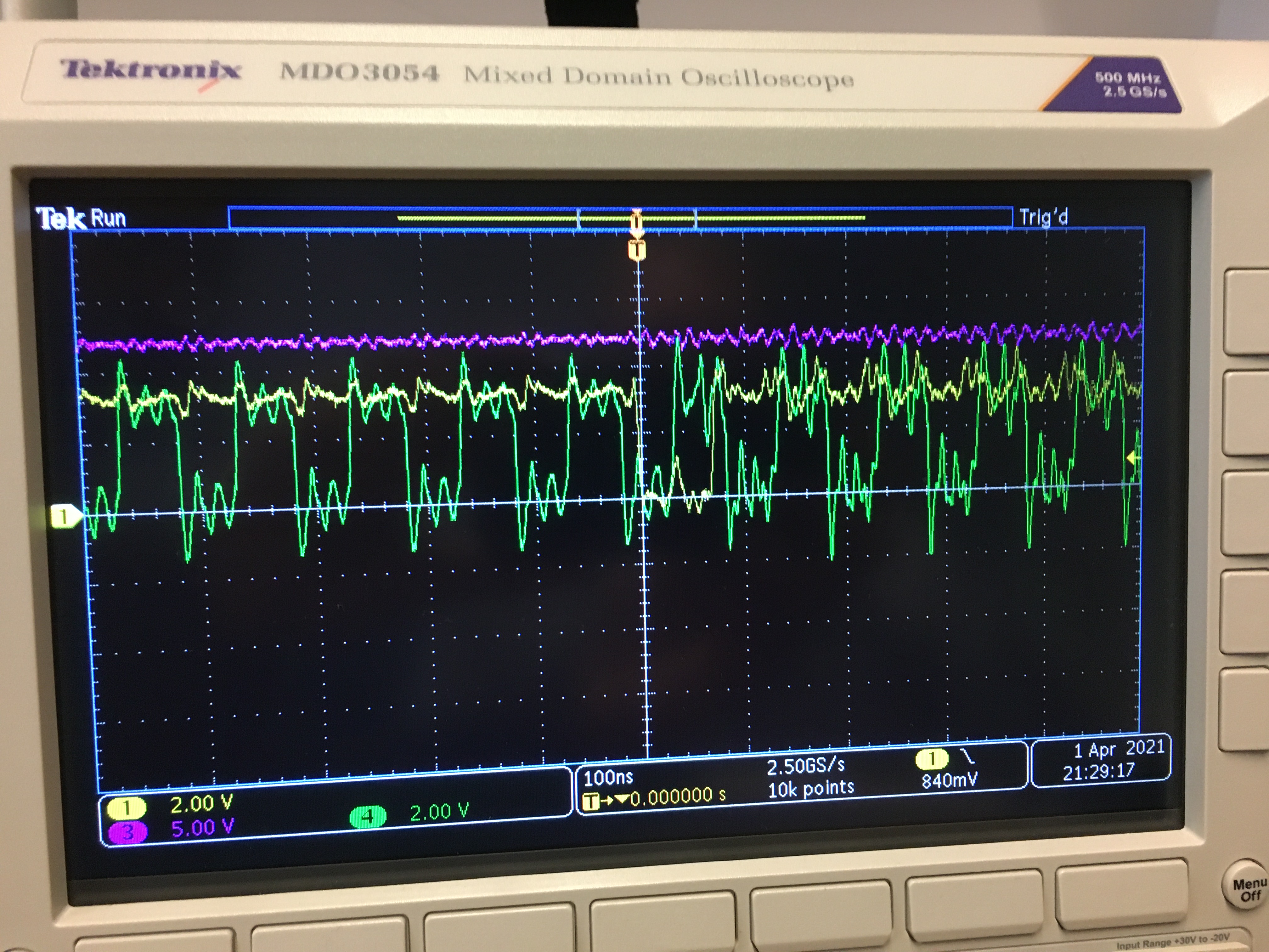 |
| 3 | P | Yellow trace shows DVALID at FPGA, purple trace shows DOUT at J2 of DDC232 board. | 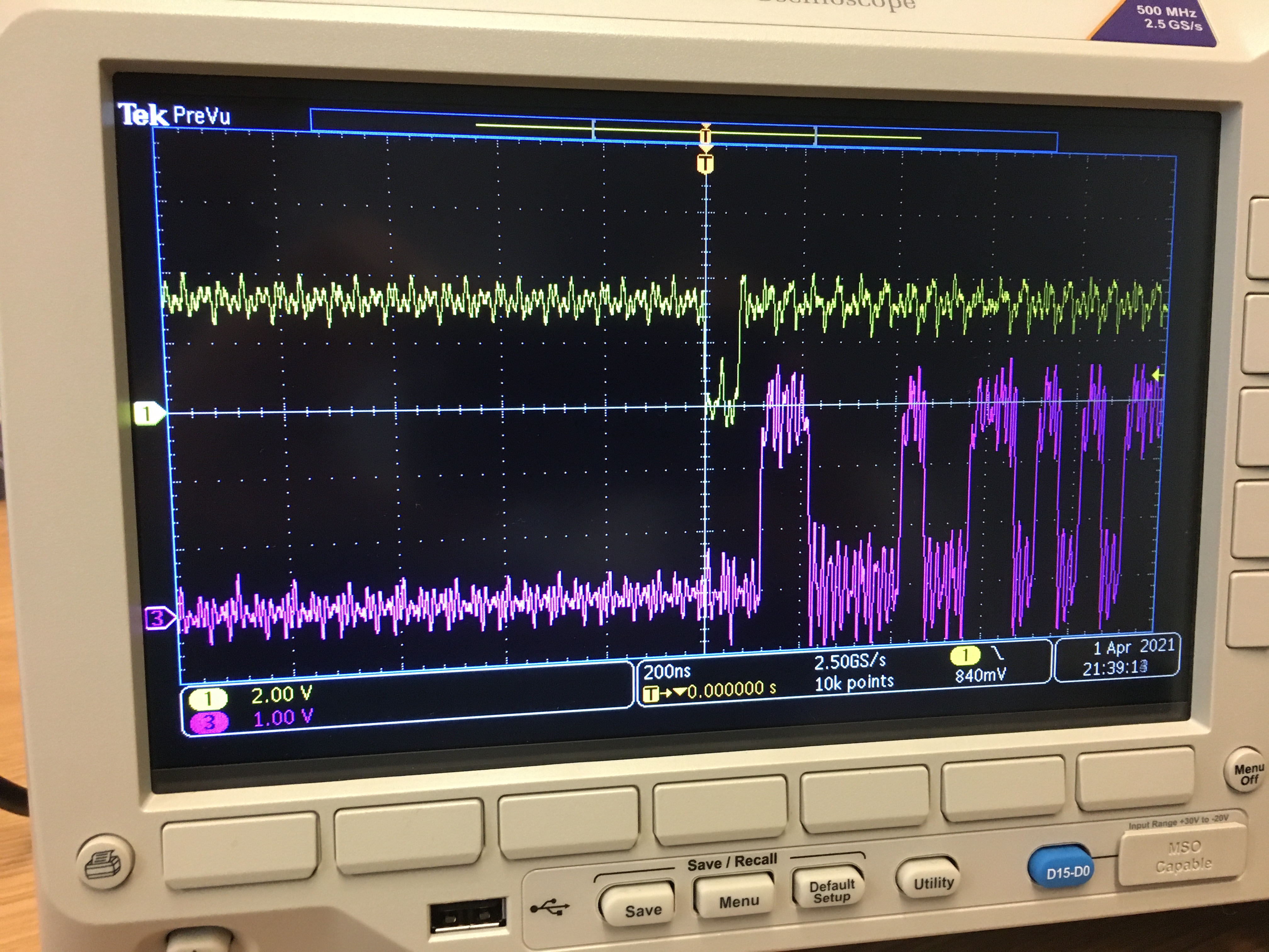 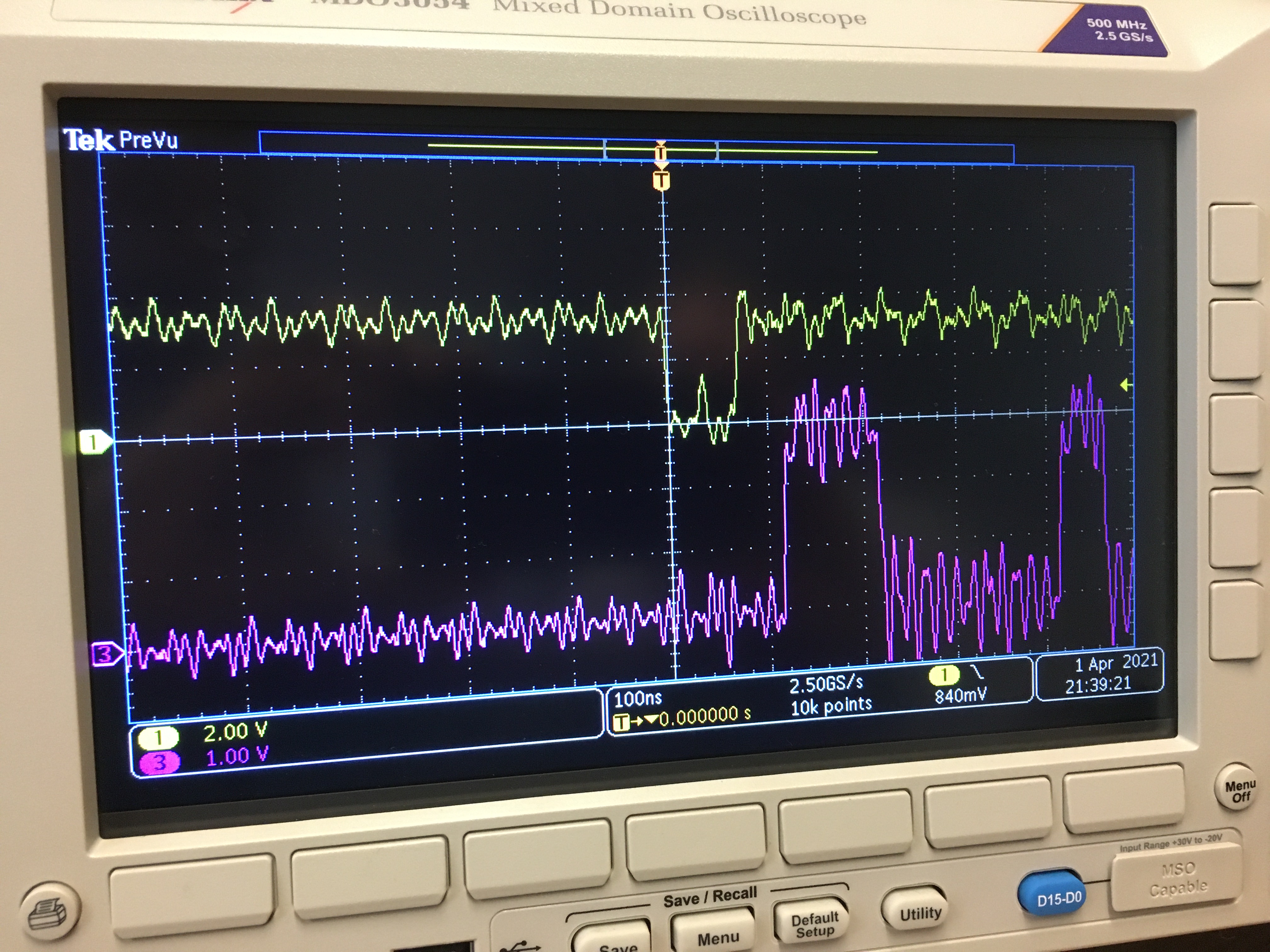 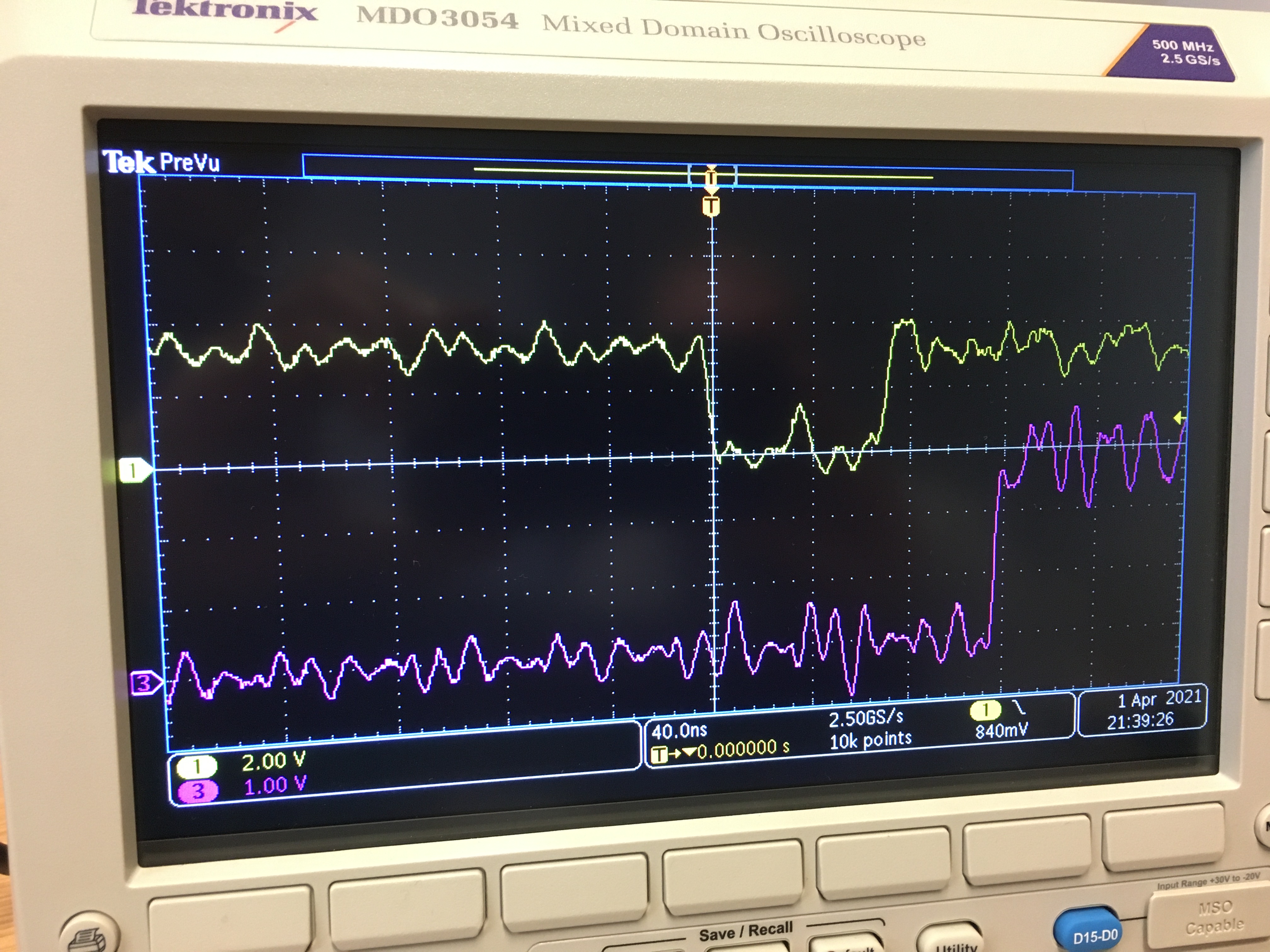 |
| 4 | P | Green trace shows CLK at J2 of DDC232 board, blue trace shows DCLK at J2 of DDC232 board. | 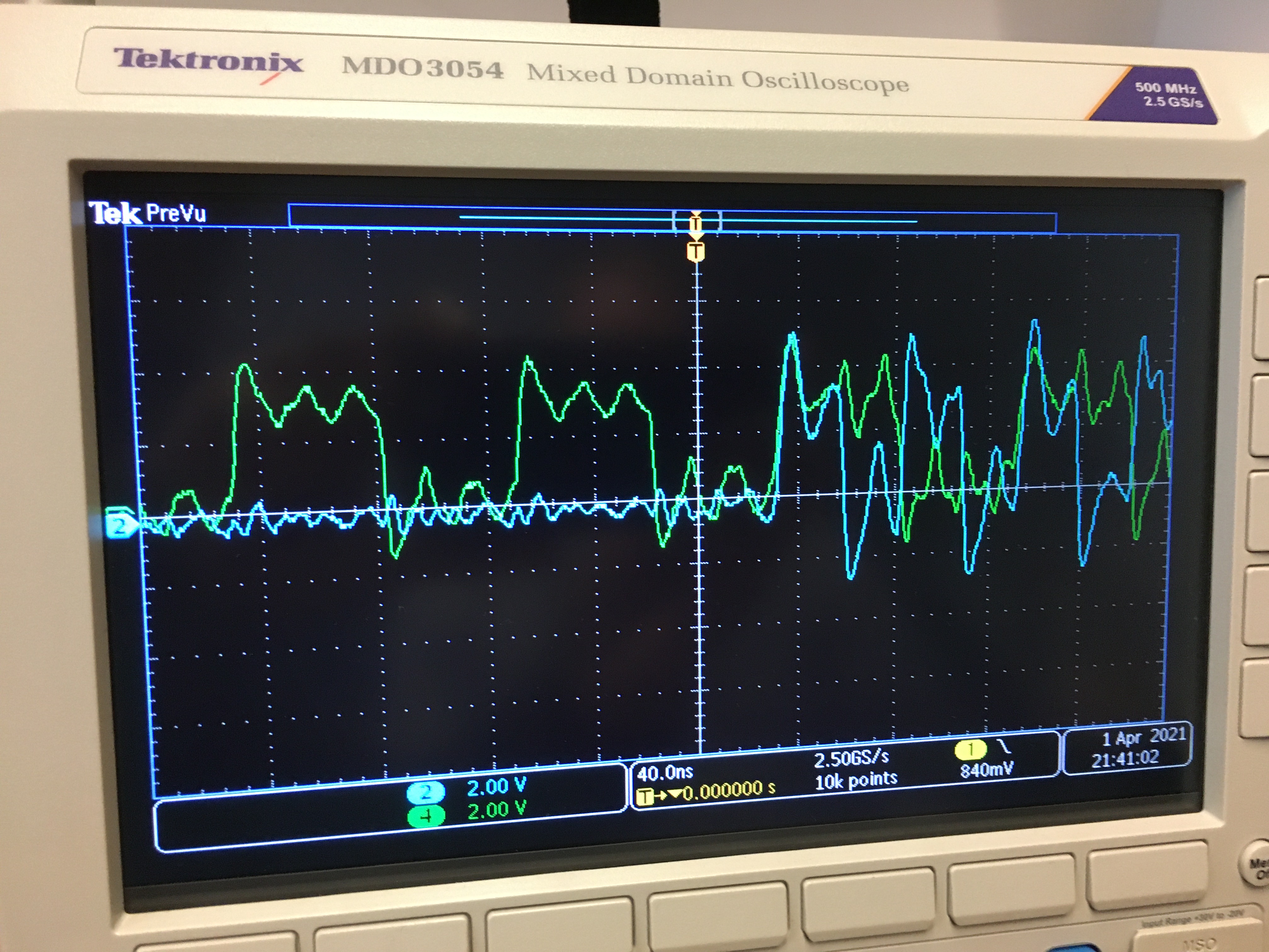 |
| 5 | P, P | Yellow trace shows DVALID at FPGA, green shows CLK of 1st board at J2, blue shows DCLK of 1st board at J2, purple shows 12V of 1st board at J2. | 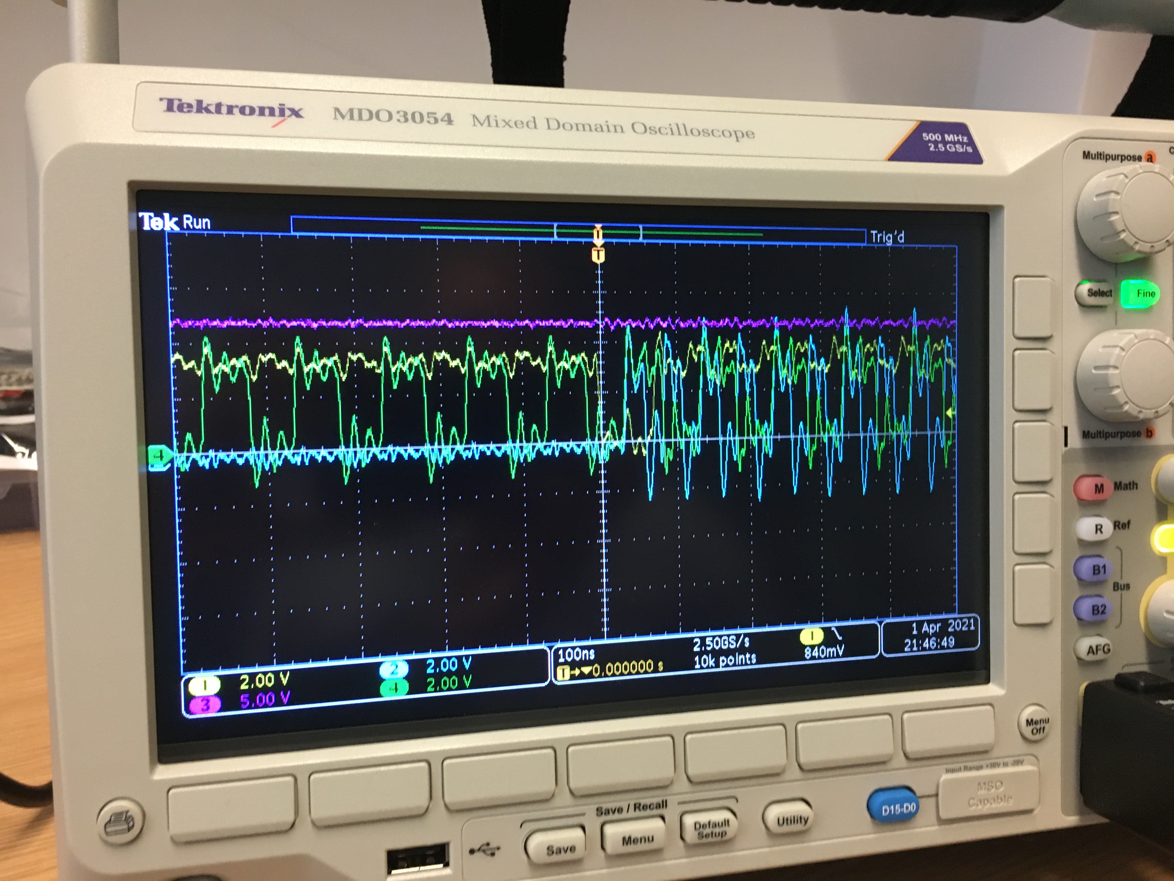 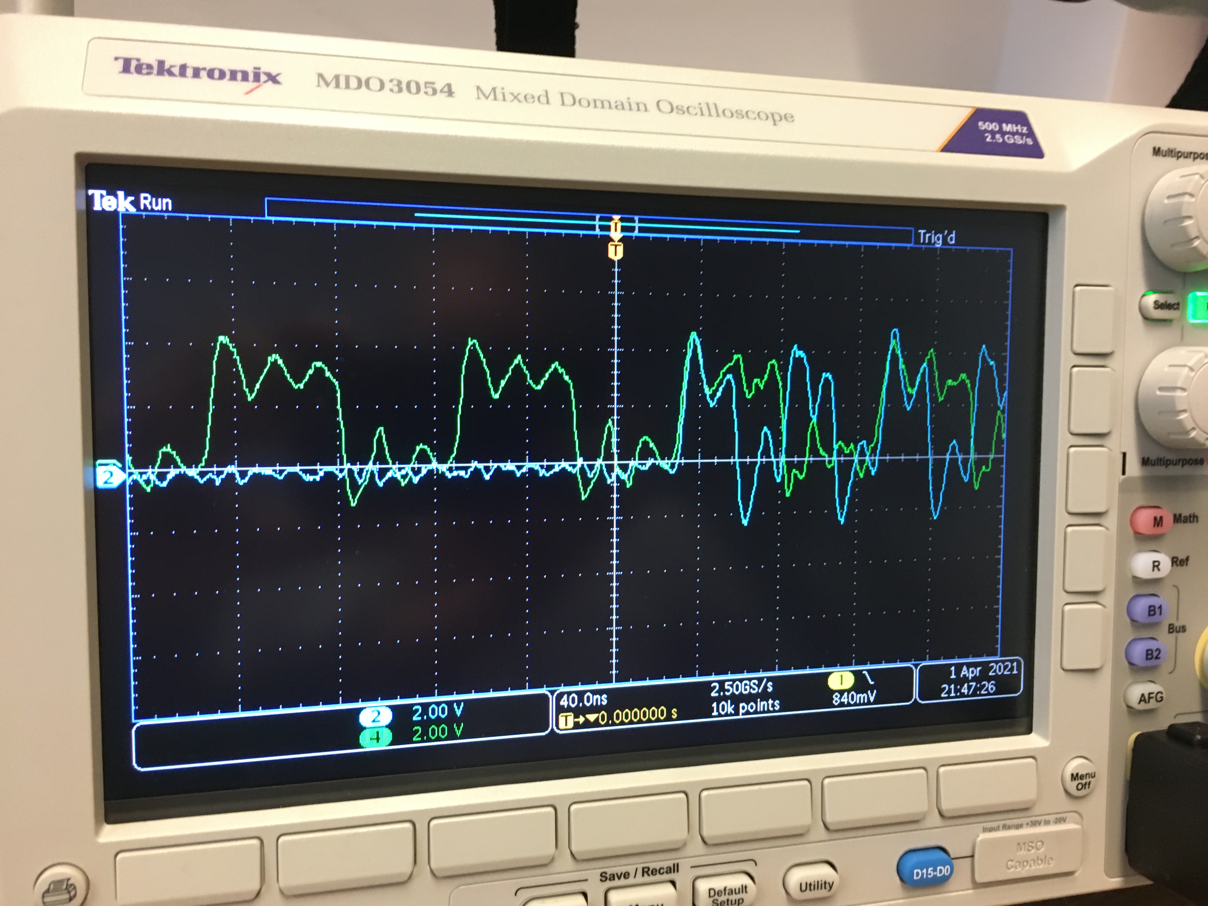 |
| 6 | P, P | Yellow trace shows DVALID at FPGA, green shows CLK of 1st board at J2, blue shows DCLK of 1st board at J2, purple shows DOUT of 1st board at J2. The last trace shows the end of a readout cycle. | 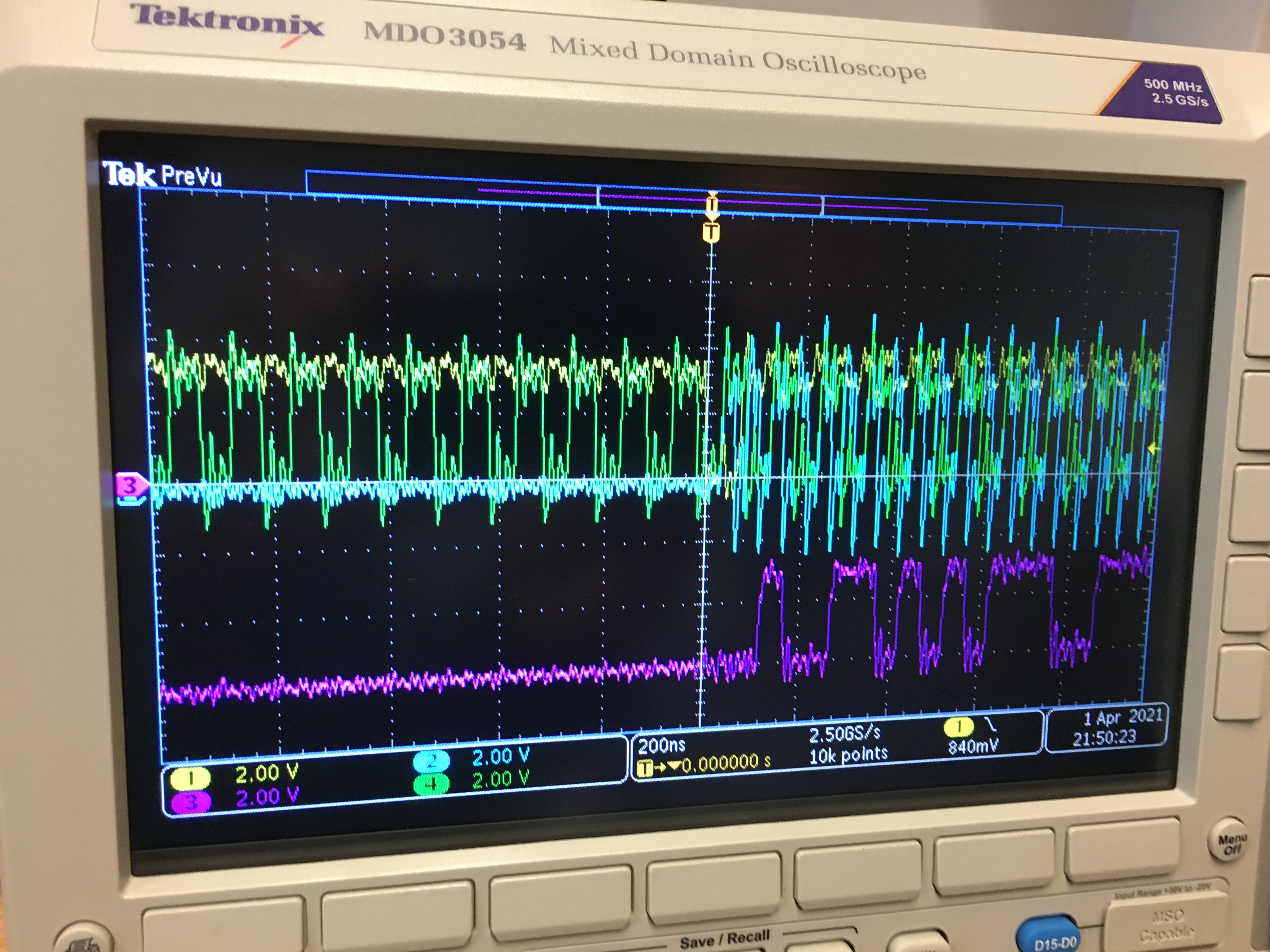 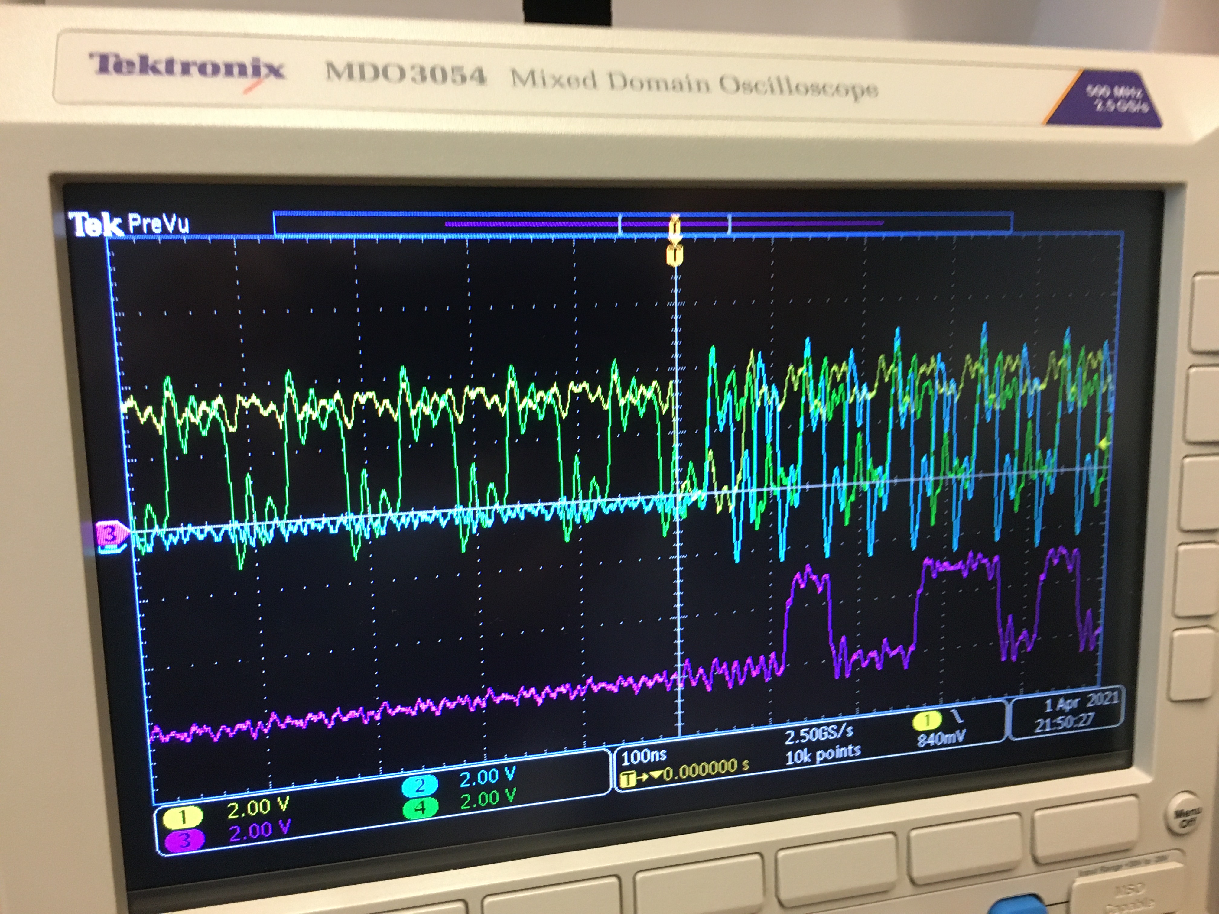 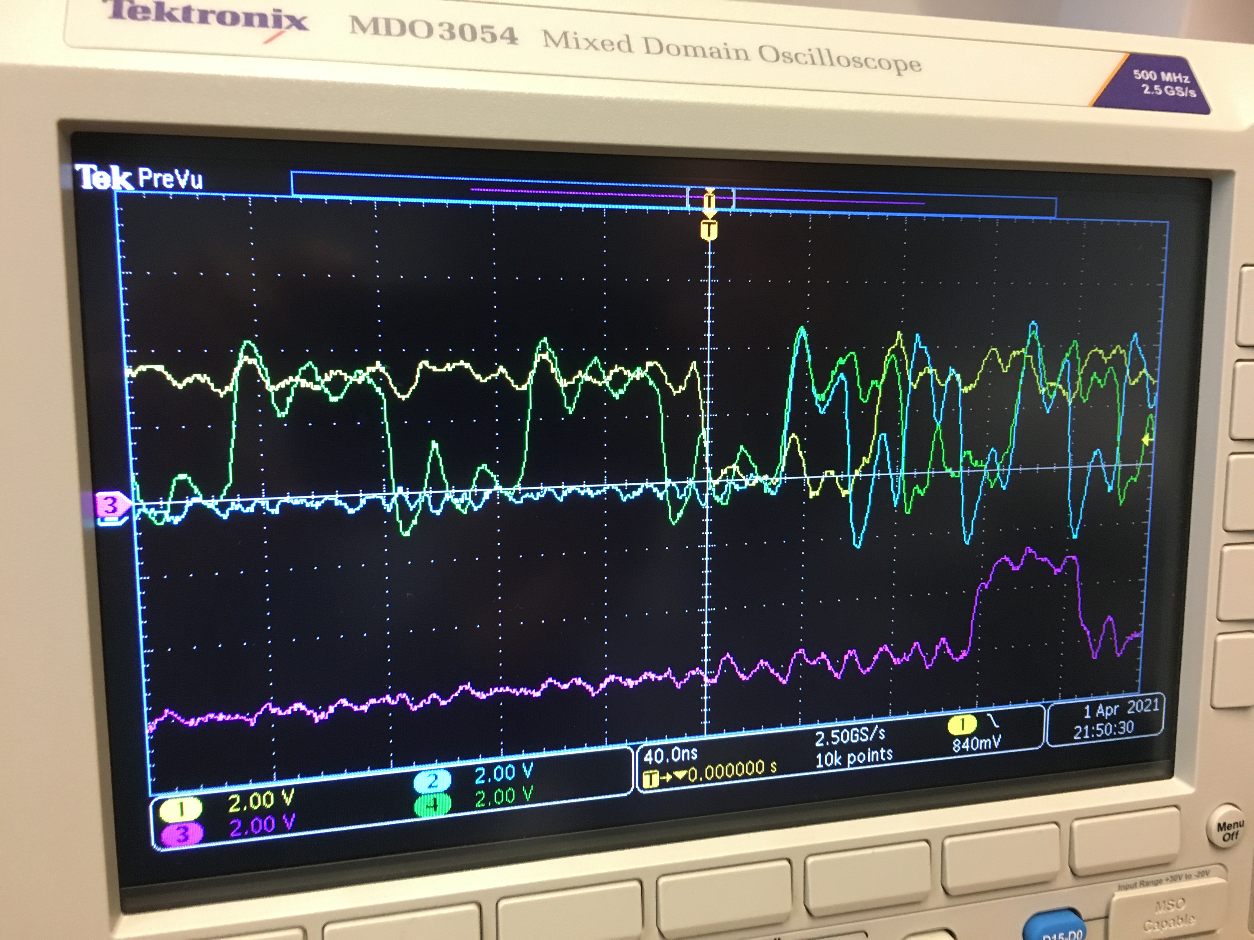 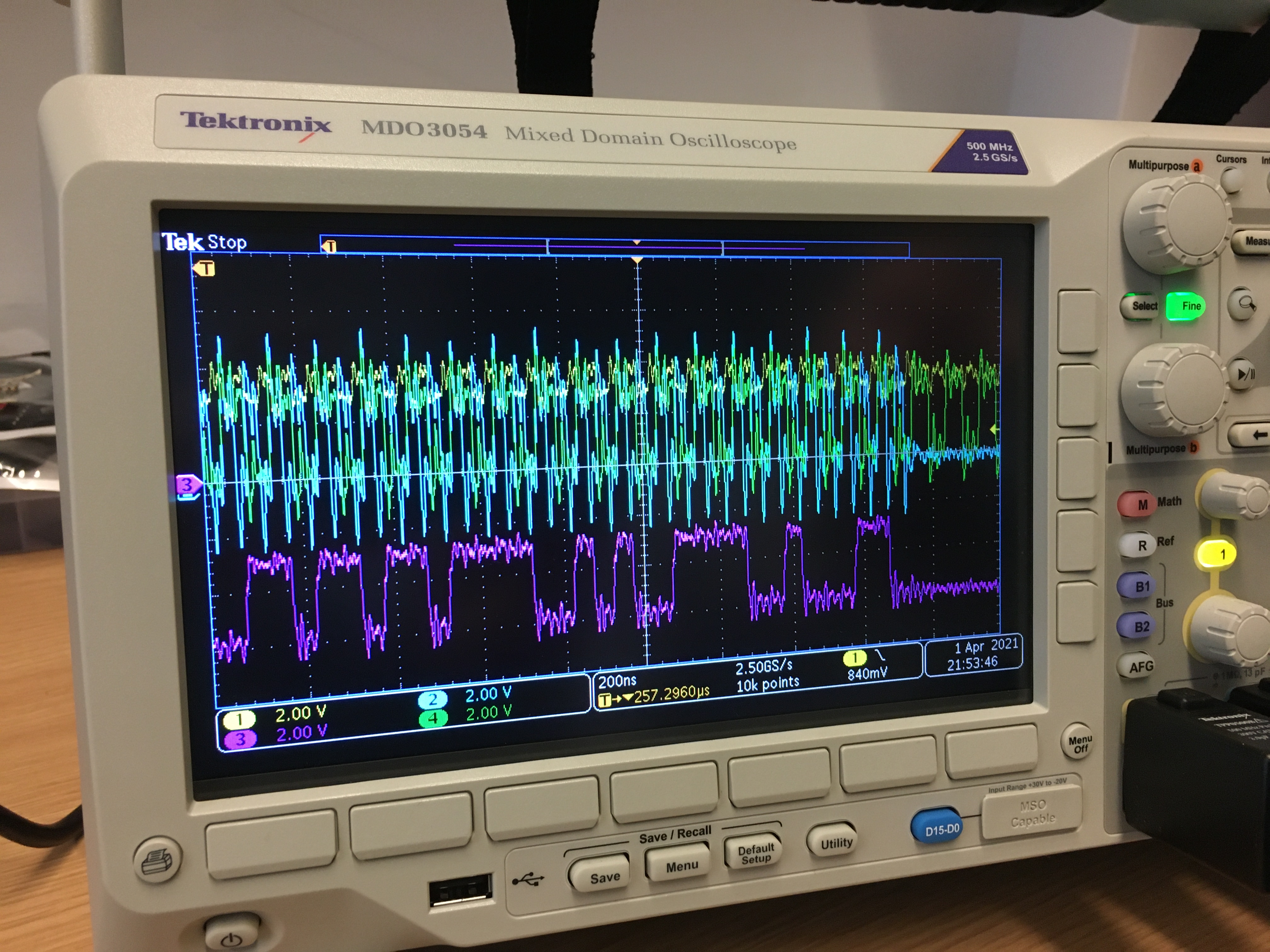 |
| 7 | P, R | Yellow trace shows DVALID at FPGA, green shows CLK of 1st board at J2, blue shows DCLK of 1st board at J2, purple shows DOUT of 1st board at J2. The trace shows the transition from photodiode data bits to resistor data bits in the readout cycle. | 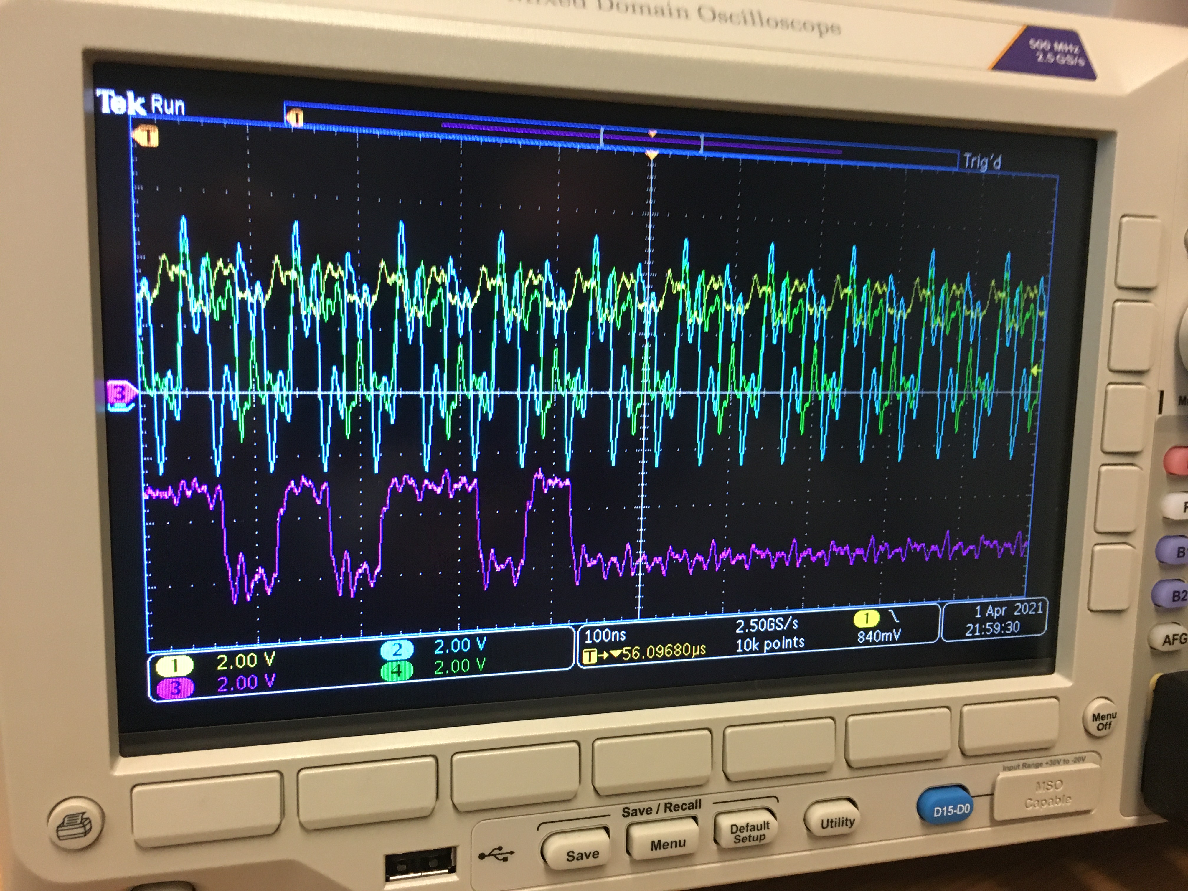 |
| 8 | P, P, P | Yellow trace shows DVALID at FPGA, green shows CLK of 1st board at J2, purple shows 12V of 1st board at J2. | 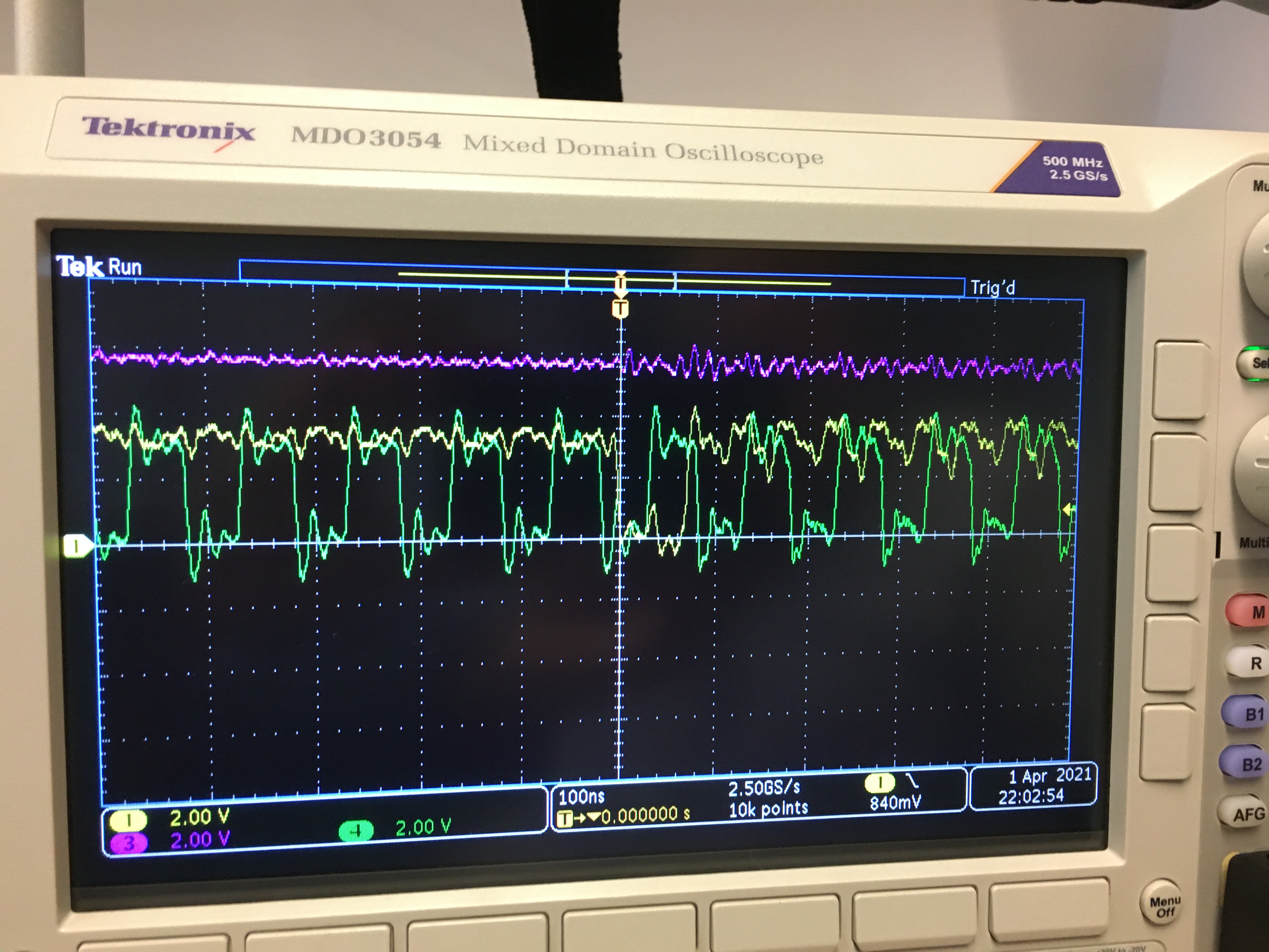 |
| 9 | P, P, P | Green trace shows CLK of 1st board at J2, blue shows DCLK of first board at J2. | 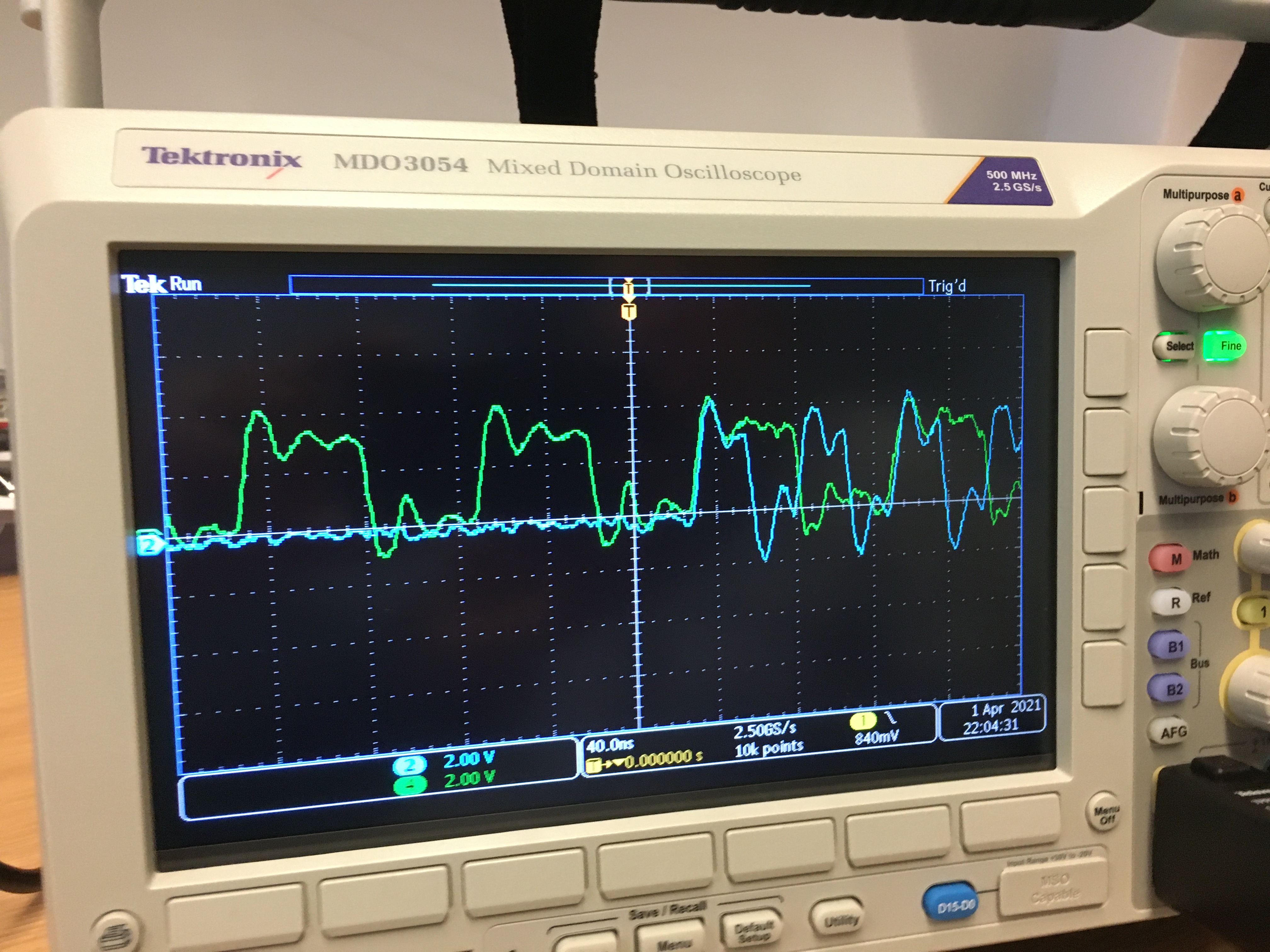 |
| 10 | P, P, P | Yellow trace shows DVALID at FPGA, green shows CLK of first board at J2, blue shows DCLK of 1st board at J2, purple shows DOUT of 1st board at J2. | 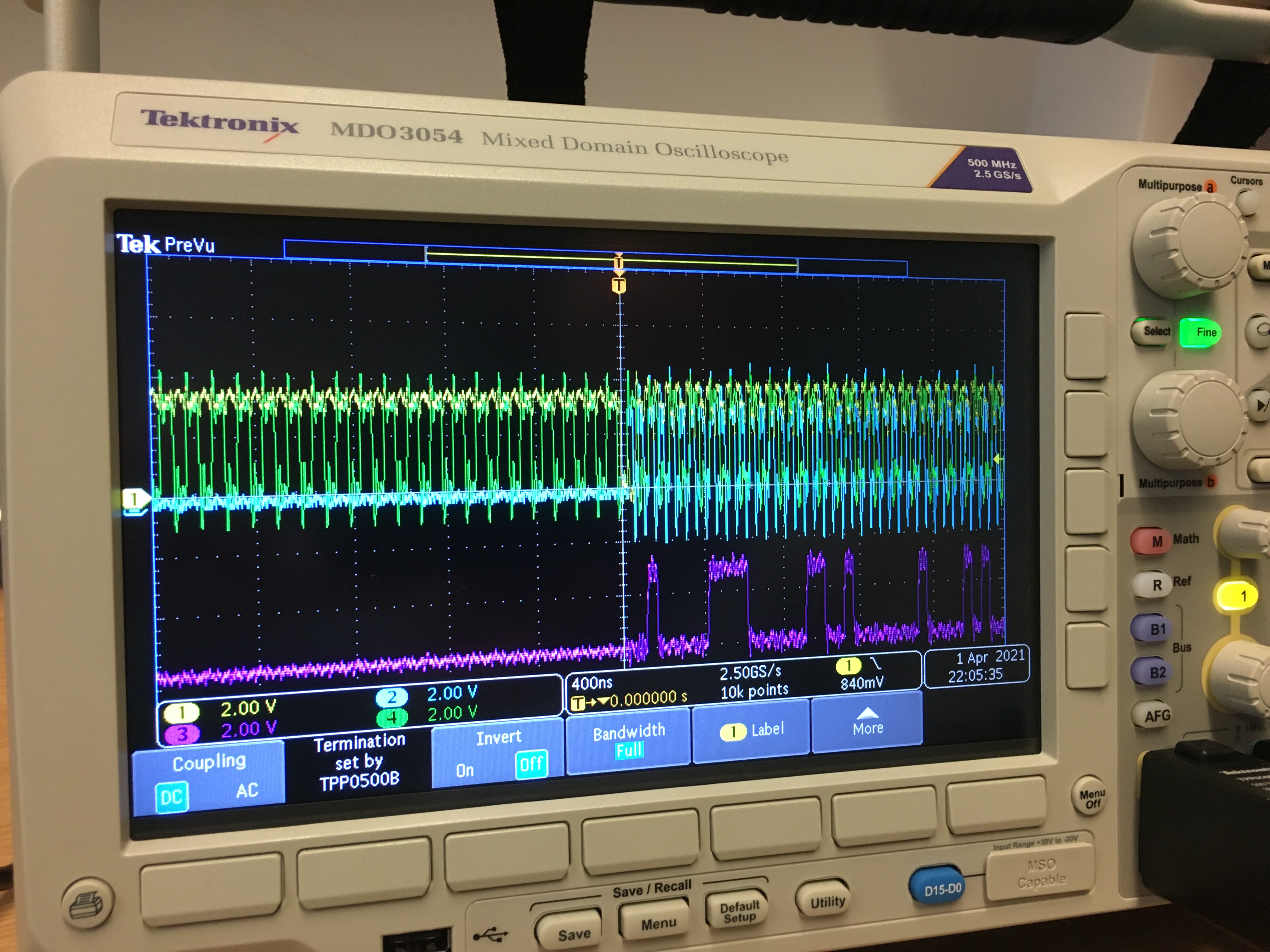 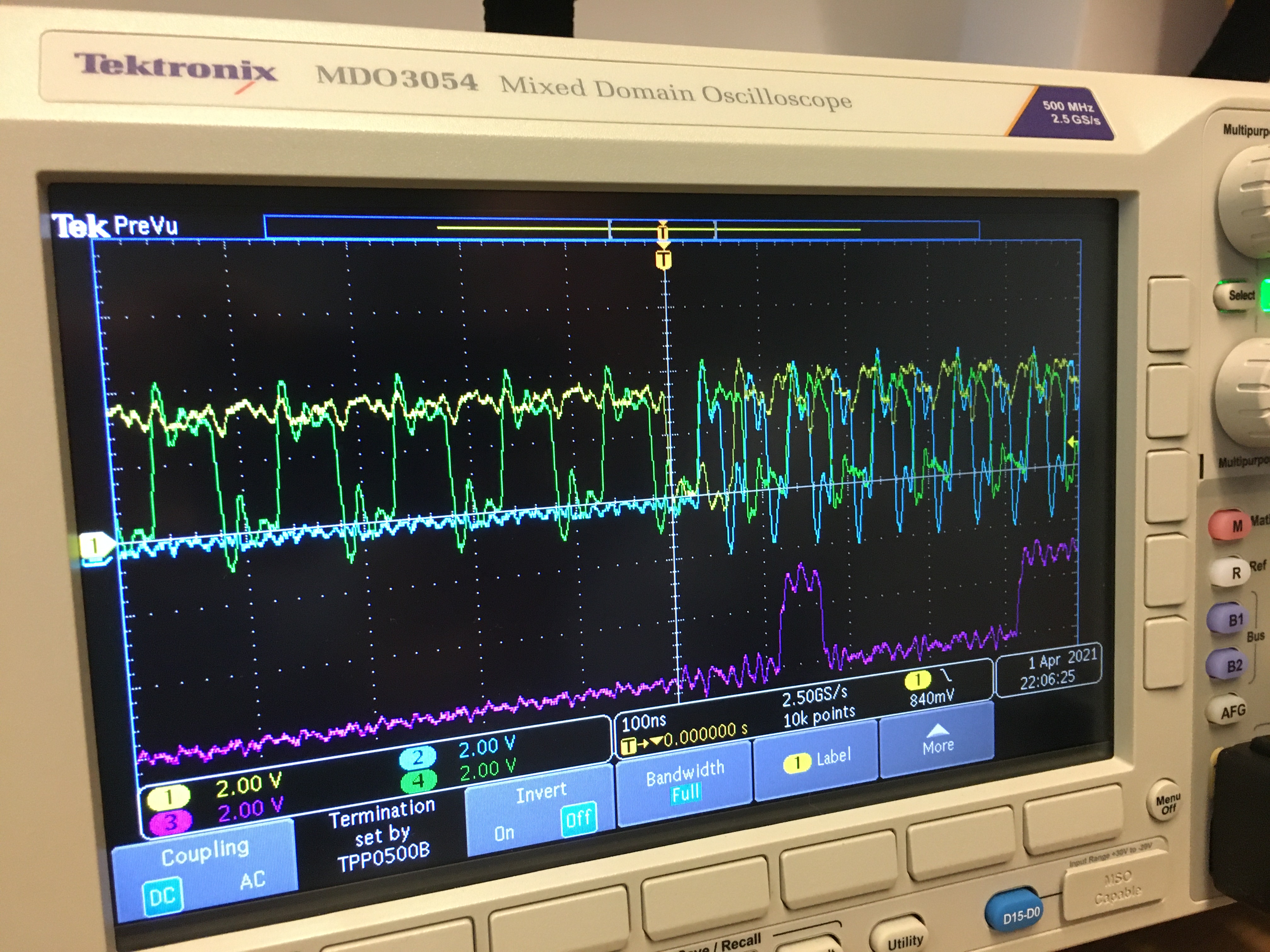 |
| 11 | P, R, P | Blue trace shows DOUT of first board at J2, purple shows DOUT of second board at J3, green shows DOUT of third at J3 | 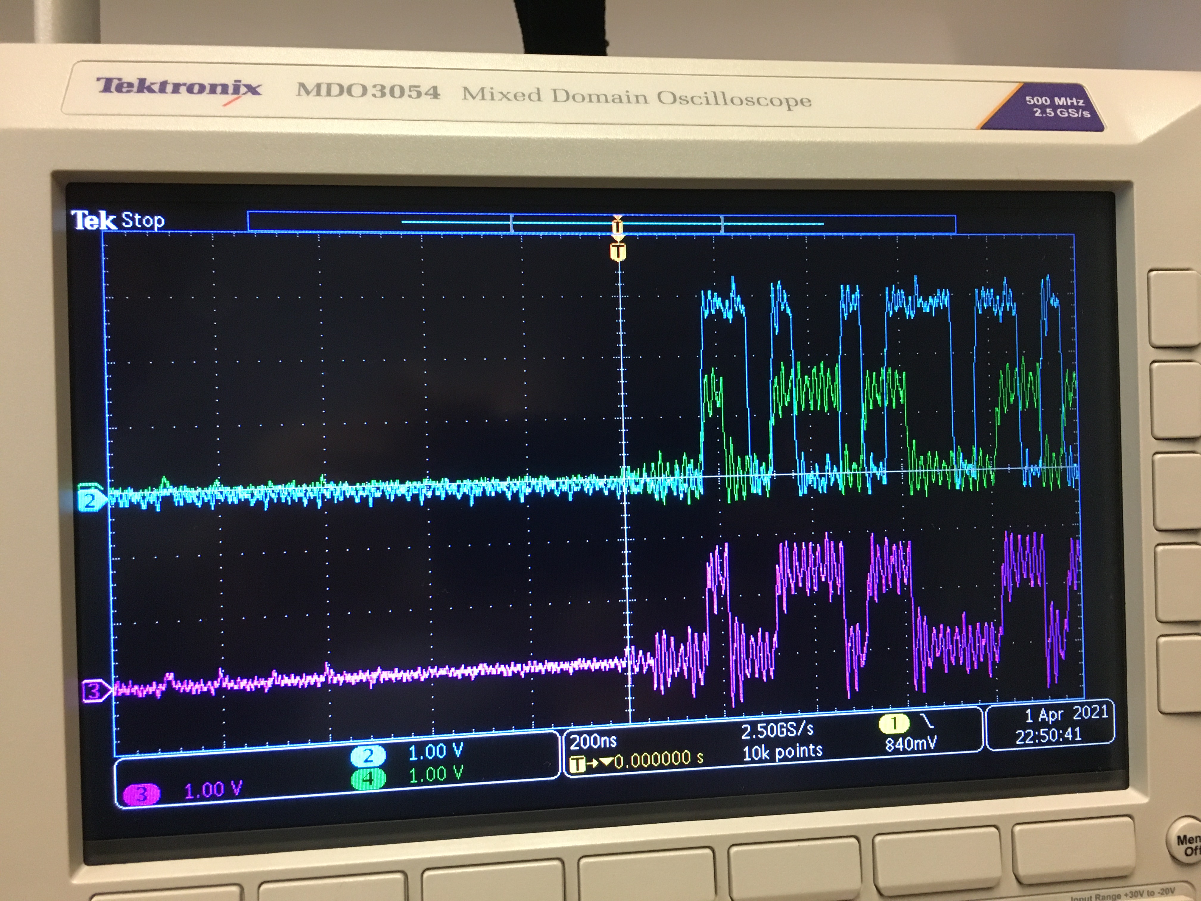 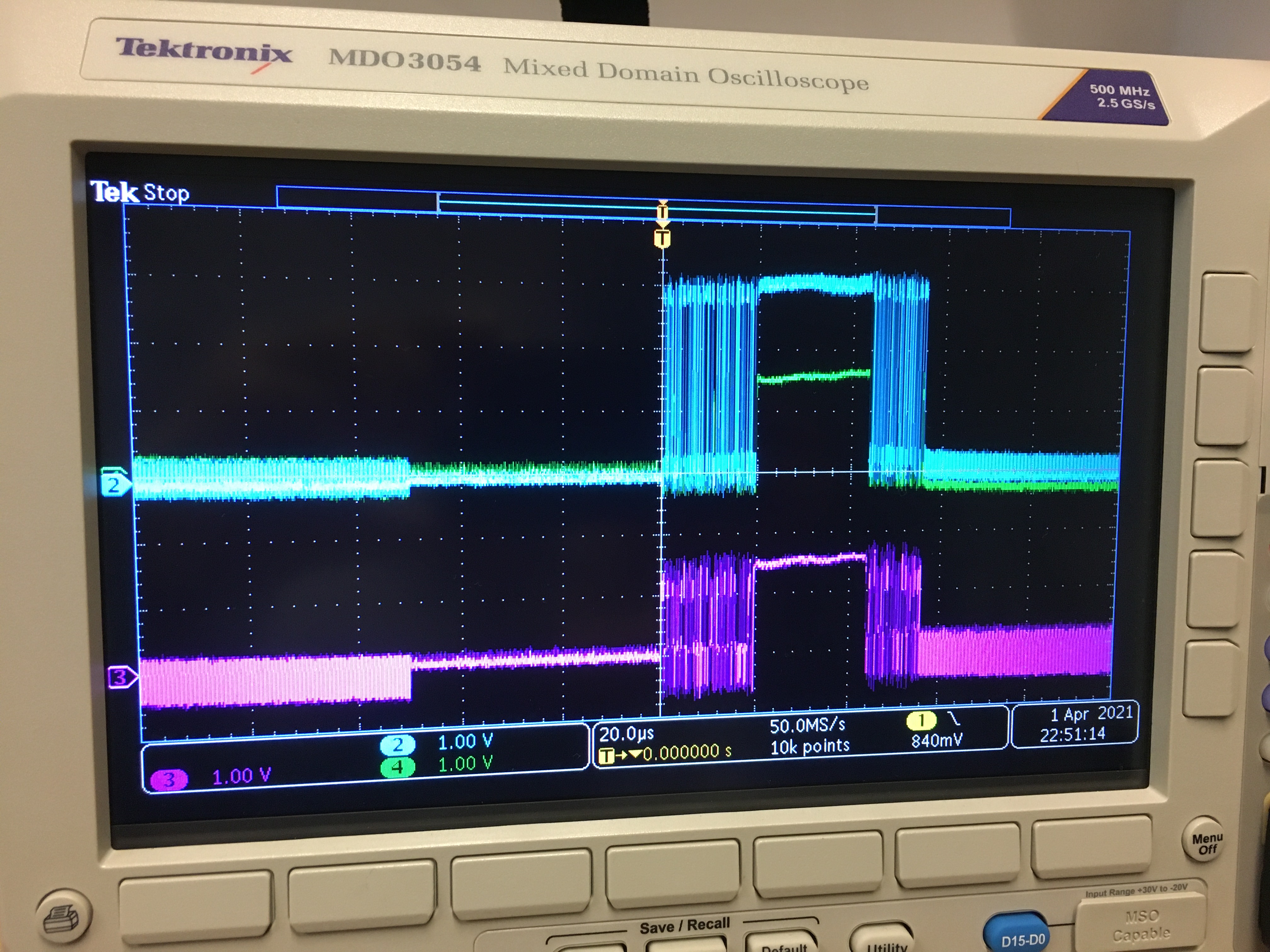 |
| 12 | P, P, P, R | Yellow trace shows DVALID of first board at J2, blue shows DOUT of first board at J2, purple shows CLK of third board at J3, green shows CLK of fourth board at J3. | 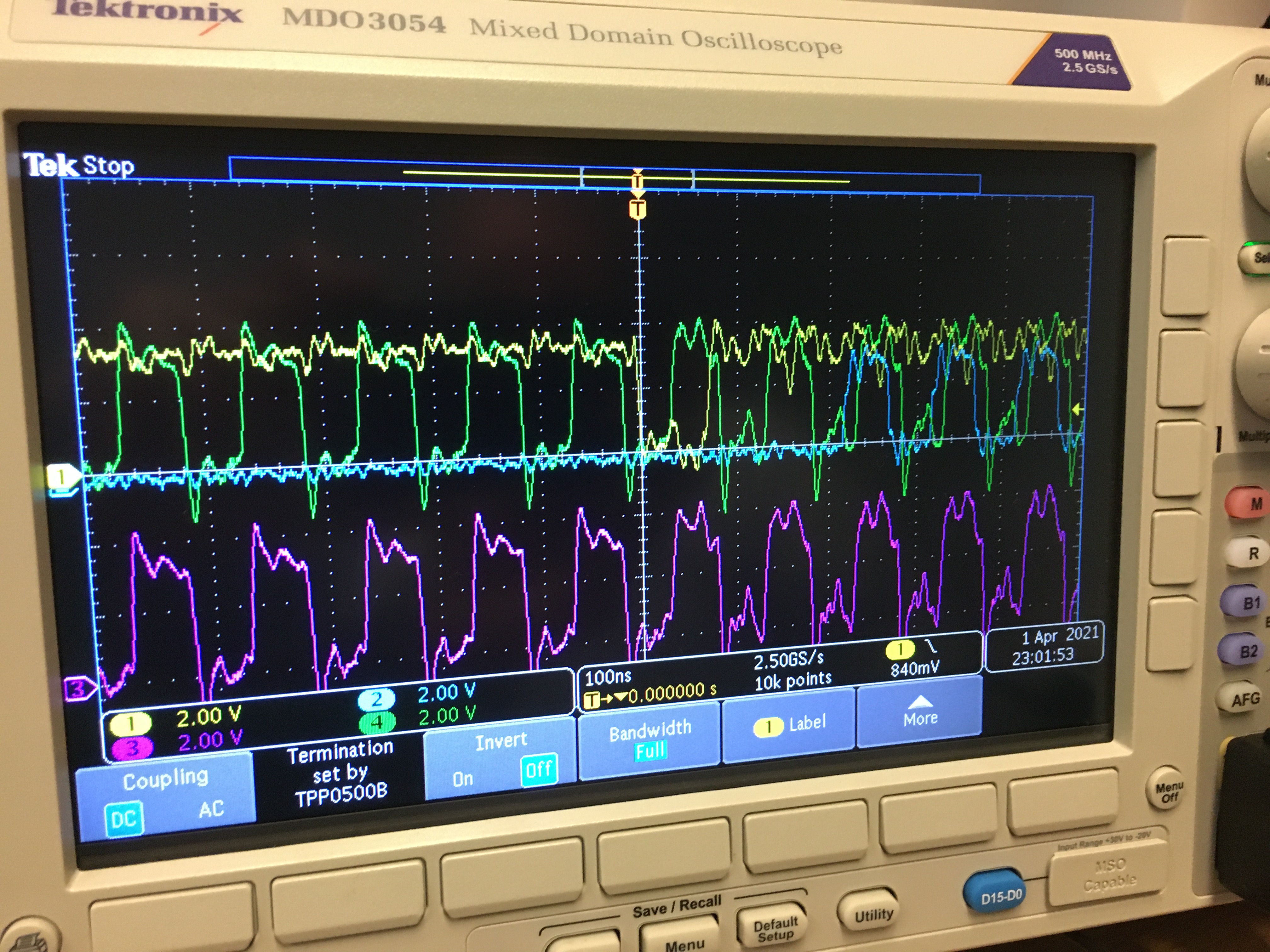 |
| 13 | P, P, P, R | Blue trace shows DOUT of first board at J2, purple shows DOUT of third board at J3, green shows DOUT of fourth board at J3. | 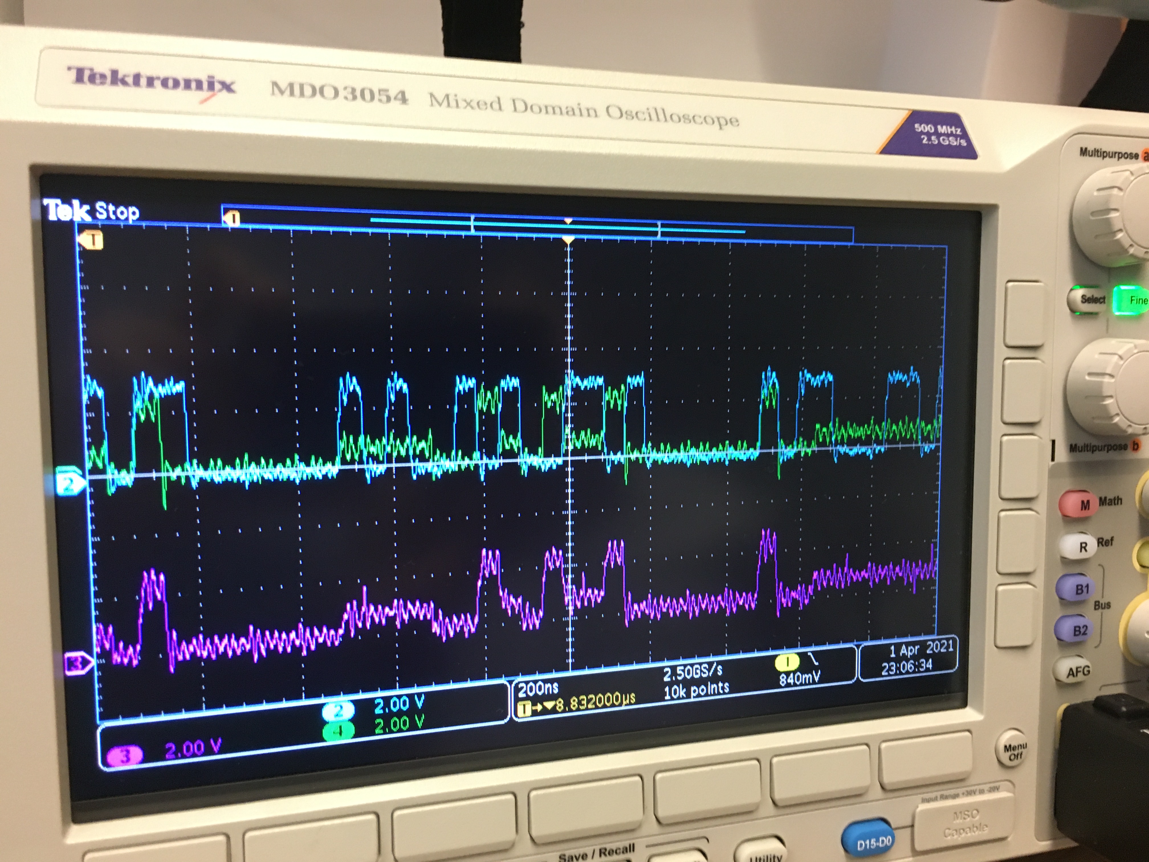 |
| 14 | P, P, P, R | Yellow trace shows DVALID of first board at J2, blue shows DCLK of first board at J2, purple shows DCLK of third board at J3, green shows DCLK of fourth board at J3. | 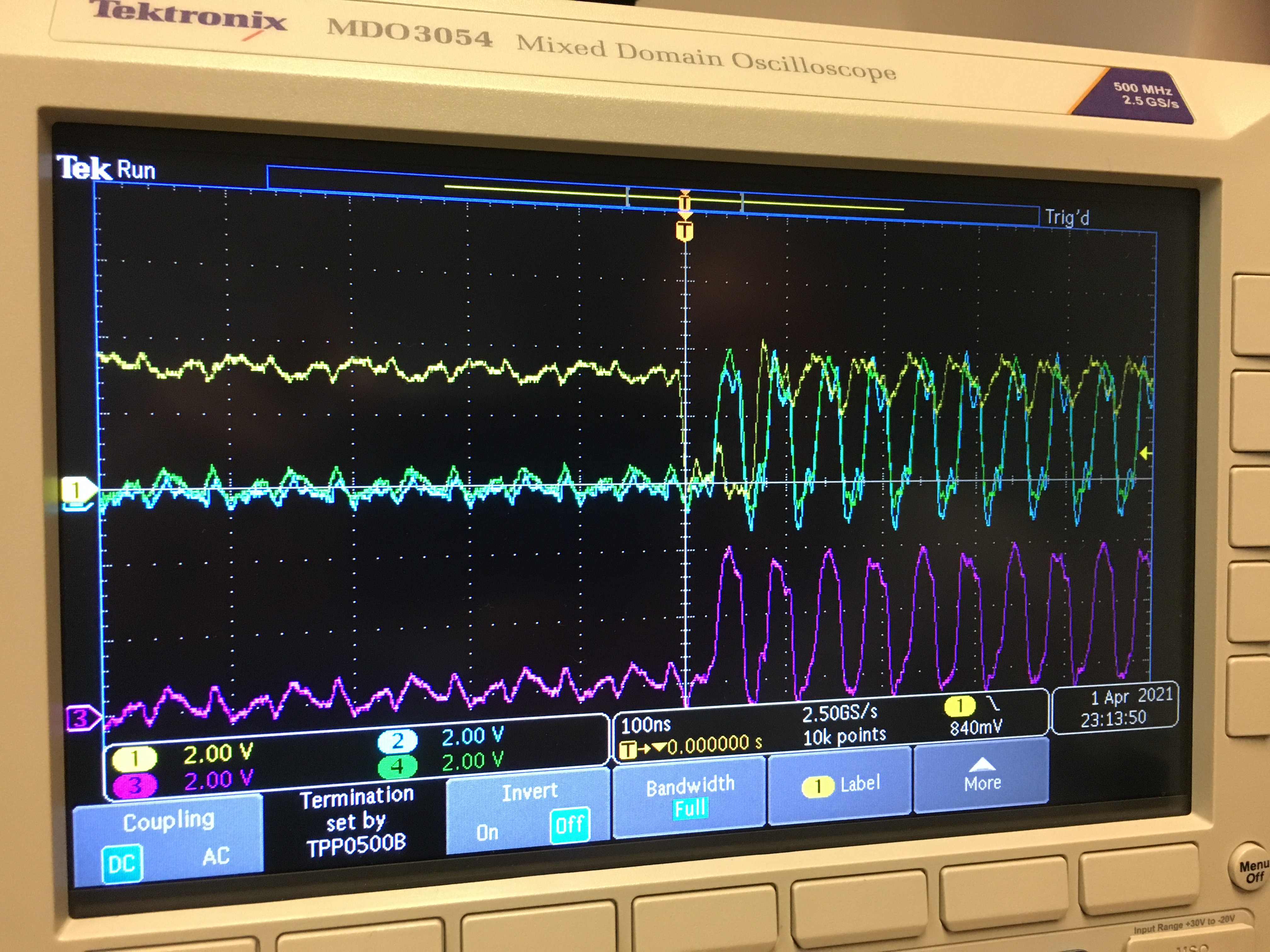 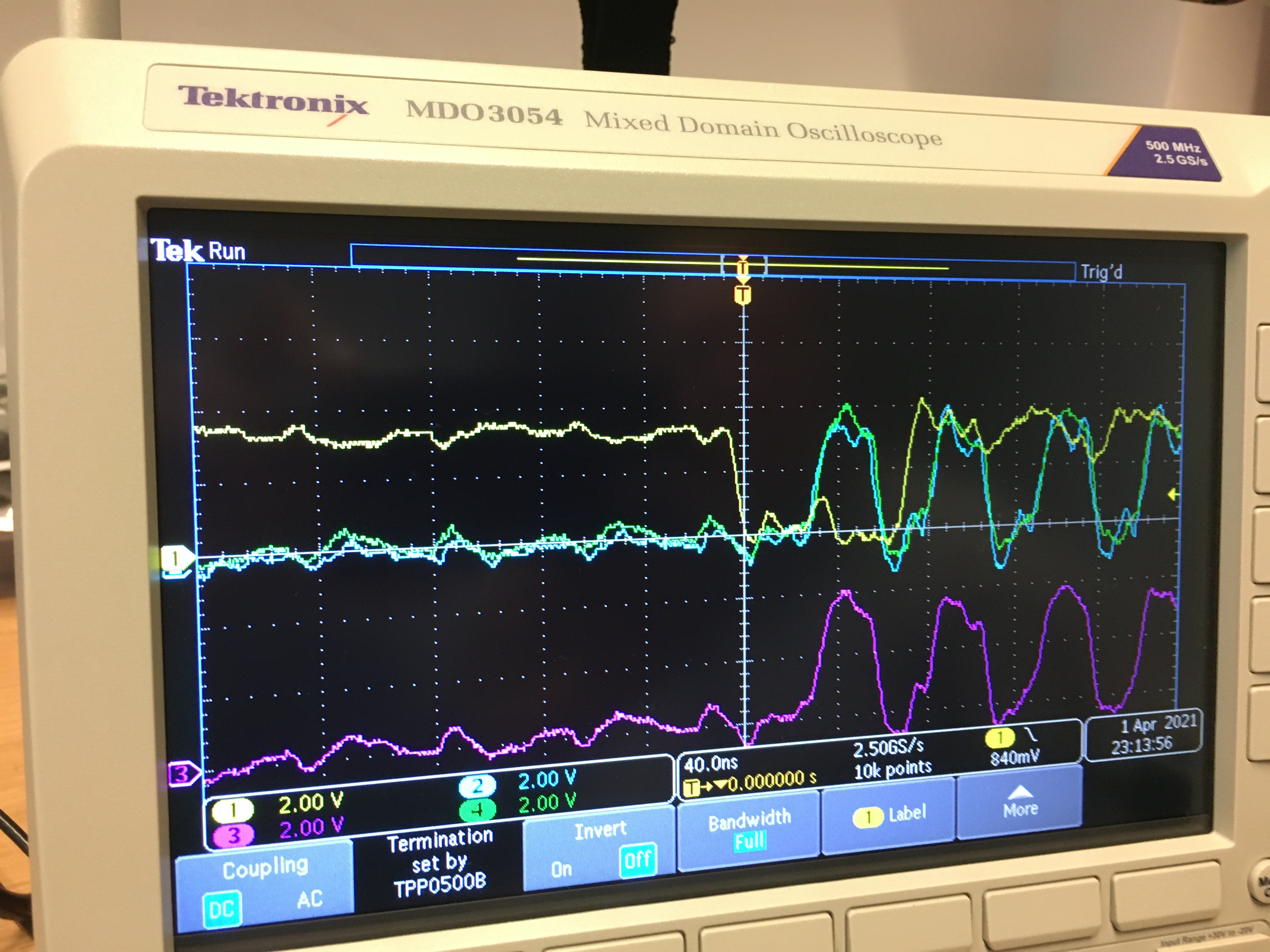 |
| 15 | P, P, P, R | Yellow trace shows DVALID of first board at J2, blue shows 12V of first board at J2, purple shows DCLK of third board J3, green shows 12V of fourth board at J3. Second image has yellow and purple showing DCLK of different boards (unsure which ones). | 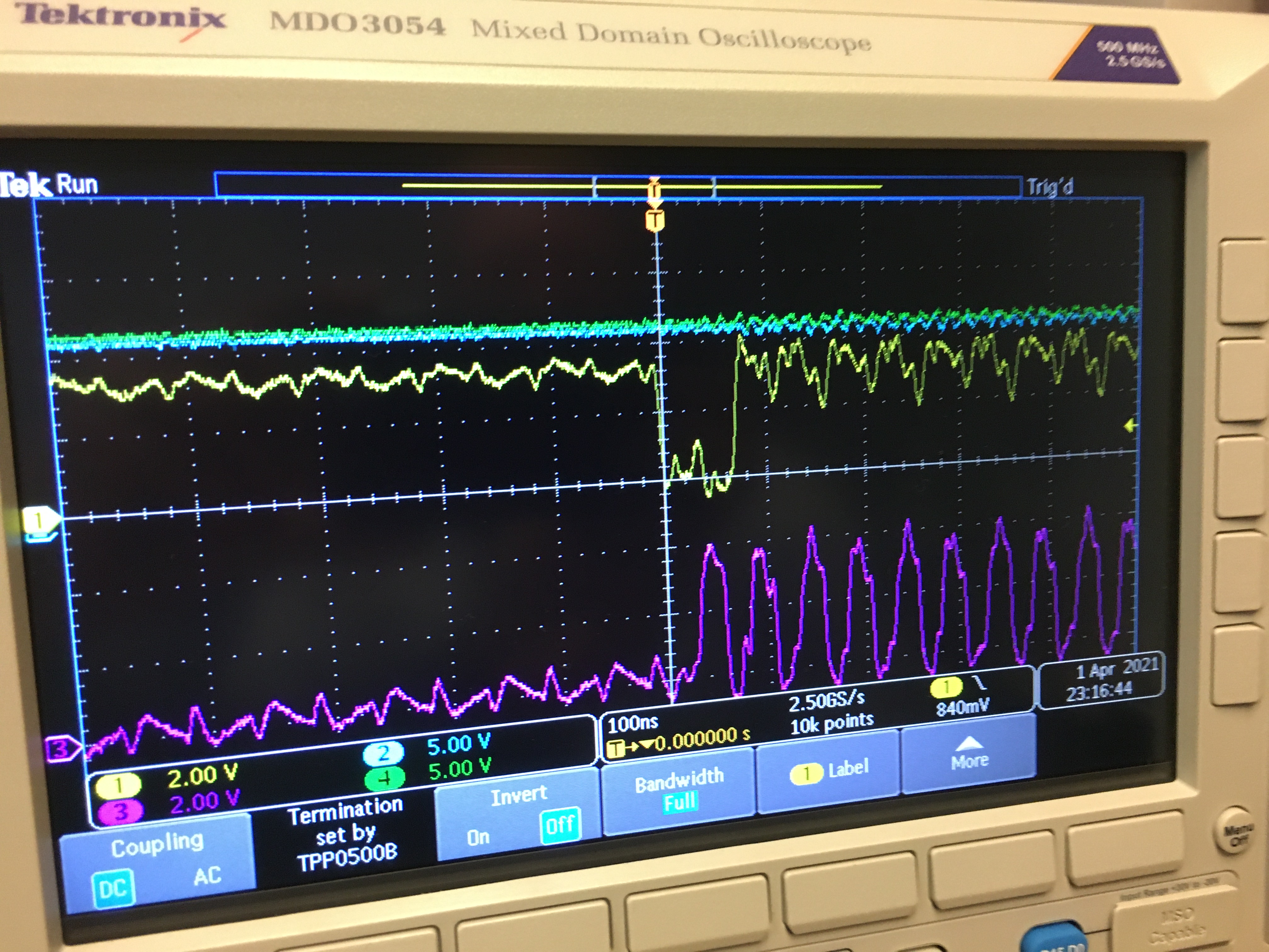 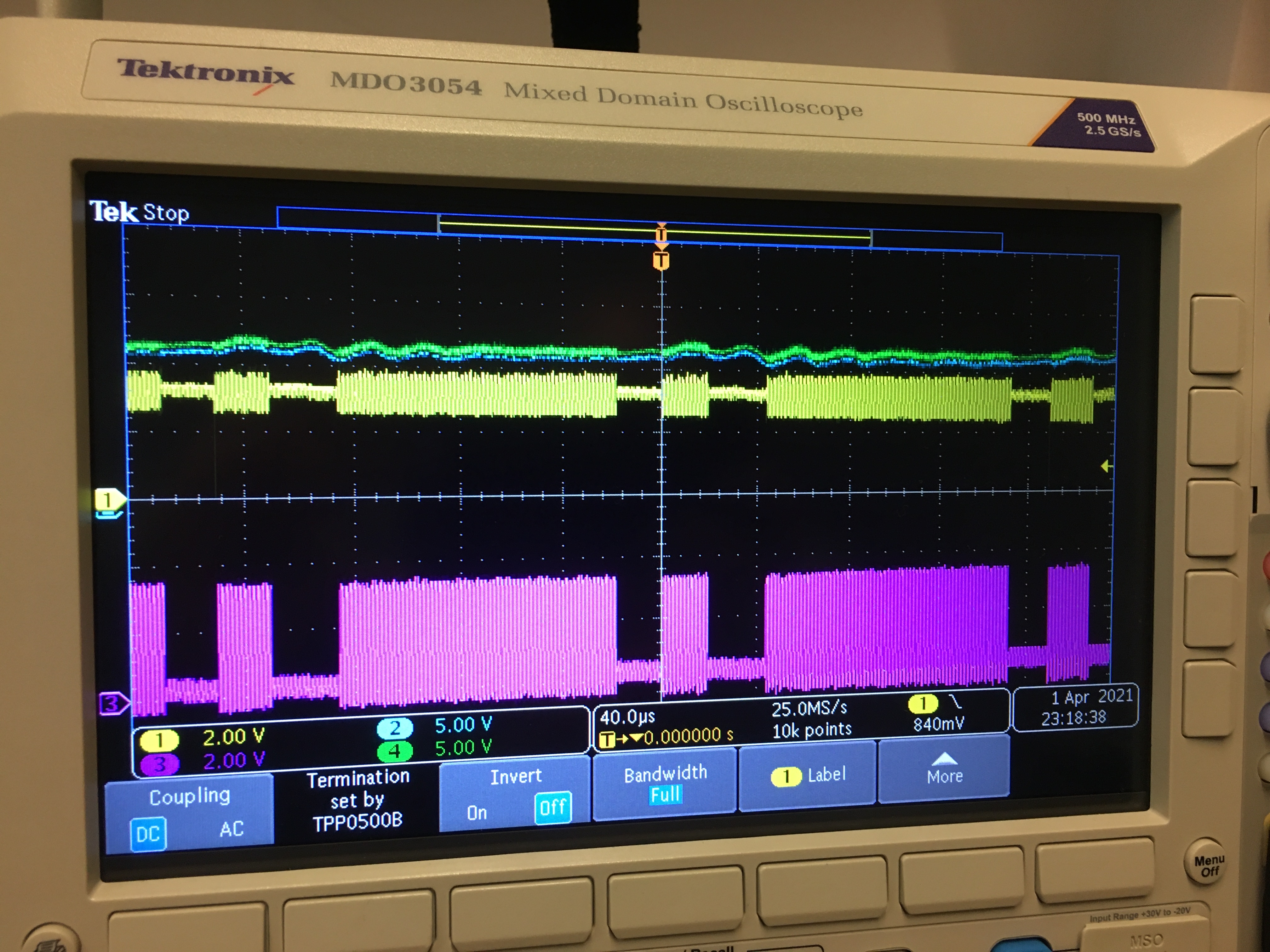 |
| 16 | N/A | Yellow shows CLK pin directly from FPGA without any board connected. | 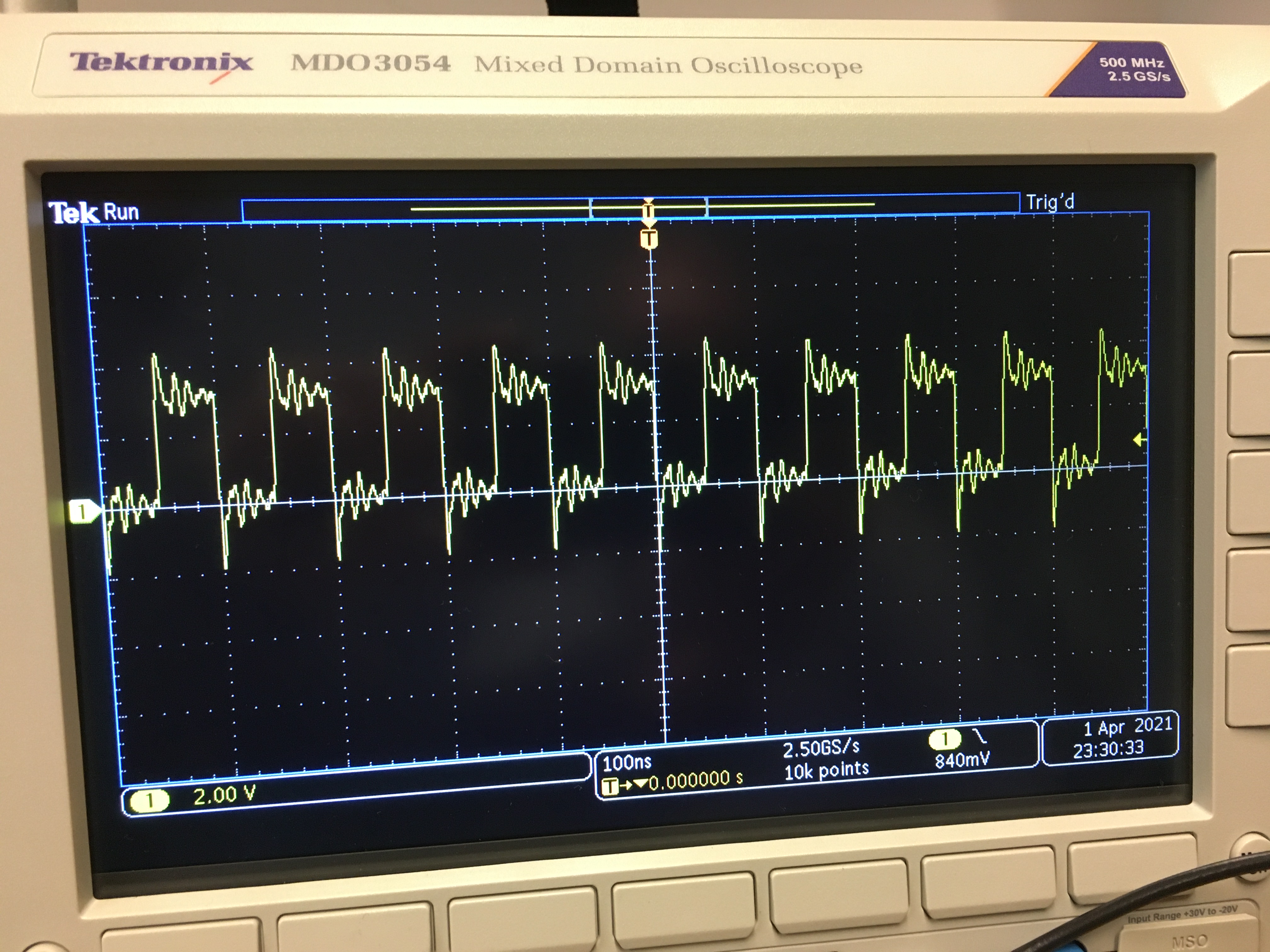 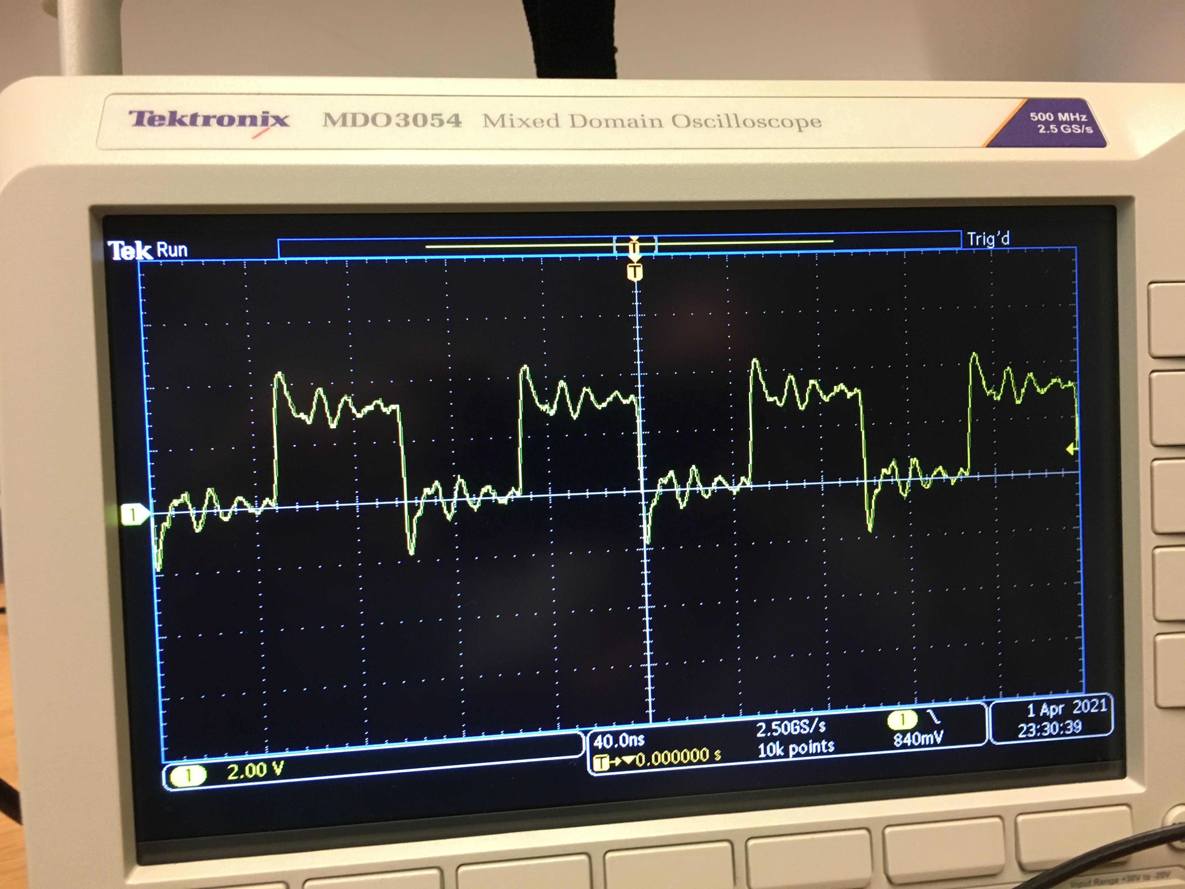 |