Maintaining the nanometre-level collisions at the IP is vital to the success of the NLC. While every attempt is made in the accelerator design to maximise the luminosity, through various design refinements mentioned in the previous chapter, a number of factors can lead to significant luminosity degradation, resulting primarily from the vibration of the linac across a large frequency range. Since the vertical beam size at the IP is only 2.7 nm, this places strict tolerances on the vertical motion of the various linac components. To compensate for this luminosity loss, the NLC employs a number of different slow and fast feedback systems. These feedback systems are each designed to address a different cause of luminosity loss and cover a range of frequencies and operating conditions. In addition to the position feedback systems described below, a number of other feedbacks are also utilised to control other features of the beam e.g. beam energy and gun current: for details of these other feedbacks, see [6] and [13]
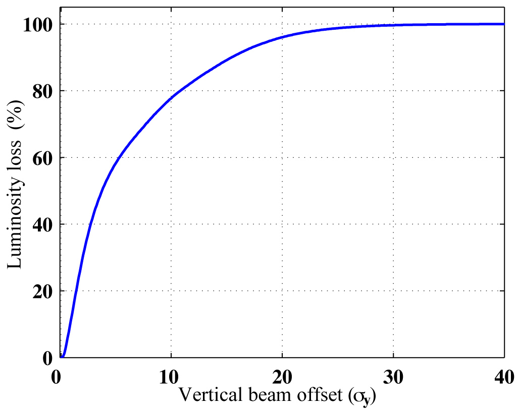
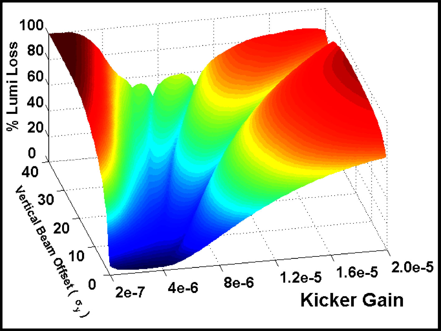
| Figure 3.1: The simulated luminosity loss as a function of the relative beam offset at the IP of the NLC [52]. |
There are two main causes of luminosity loss, both of which are related to the alignment of the accelerator [13]. The first of these is the relative motion of the two beams at the IP. The luminosity loss as the result of a relative beam offset at the IP is shown in Fig. 3.1: since σy = 2.7 nm for the NLC Stage I, this demonstrates that the accelerator is only 20% productive for a relative beam-beam offset of just 30 nm. The cause of these offsets lies in the transverse motion of the beam, as a result of the dynamic motion of the accelerator components: this random beam motion is referred to as beam jitter. Luminosity degradation also results from an increase in beam emittance caused by misalignments of the accelerating structures. The wakefields created by the passage of a bunch train through a structure (see Section 2.3.3) will apply a transverse kick to each bunch: this kick will cause an increase in the beam spot size which cannot be removed and is called emittance dilution. While both problems have essentially the same root cause, the prevention of emittance dilution will not be dealt with here — for more information see [13].
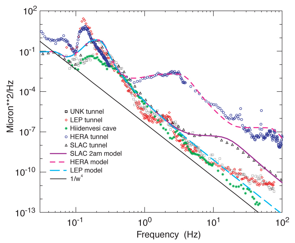
| Figure 3.2: The power spectrum of ground motion for a number of accelerator tunnels [13]. The 0.15 Hz peak in each trace is due to ocean waves; Hiidenvesi is a cave in Finland used as a reference. |
The primary source of beam jitter is the motion of quadrupoles in the main linac and the beam delivery system: this quadrupole motion accounts for more than half the beam jitter seen at the IP [13]. The main cause of such quadrupole vibration is the natural ground motion of the NLC site (water flow within the NLC structures and amplification of the resulting vibration by the quad supports are also contributory). The power spectrum of the ground motion measured in the SLC accelerator tunnel, as well as a number of other accelerator sites, is shown in Fig. 3.2.
The noise due to ground motion is generally split into two types. Below 1 Hz, the ‘low-frequency’ motion, while of greater magnitude than higher frequency noise, is largely correlated along the length of the linac; above this frequency, the magnitude of the ‘high-frequency’ motion drops rapidly (see Fig. 3.2), but is no longer correlated along the linac. As such, different techniques are required to remedy each type of noise. In addition to this natural ground motion, man-made cultural noise will also cause random accelerator motion: a number of the NLC designs have therefore attempted to site the accelerator away from cultural centres [13].
The primary method of correcting the low-frequency noise is through beam-based steering feedback: this is described in the next section. Reducing the high-frequency motion sensitivity of the accelerator is achieved by careful selection of the NLC site and through optimising the design of the accelerator support structure [6]. Careful design of the RF girders and the quadrupole supports is required to prevent excess vibration, particularly due to man-made sources within the accelerator (such as vibration from cooling systems) to reduce the contribution to the high-frequency jitter.
Beam-based steering feedback is the most commonly utilised position feedback system. It is used to maintain the optimum orbit by adjusting the beam trajectory at various points along the linac. The beam orbit is monitored with a series of beam positions monitors (BPM's — see Section 4.1) mounted inside each of the quads. Pairs of dipole correctors along the linac are then used to actively correct the orbit in response to the position measured by the BPM's. Beam-based steering feedback was originally employed at the SLC as a method of correcting the low-frequency beam motion [53]. The system was a database-oriented design that was used to control a variety of beam parameters, including the beam energy and the beam intensity at the injector. A number of different algorithms were used during the running of the SLC: the database driven design allowed the rapid implementation of new feedback algorithms based on recorded beam data.
A similar system is envisaged for the NLC. With the machine repetition rate of the NLC identical to that of the SLC at 120 Hz, the systems will have similar operating parameters. The Nyquist frequency of such a system is therefore 60 Hz and allows correction of a large quantity of the uncorrelated beam jitter below 60 Hz. Like the SLC, a number of feedback algorithms are under investigation to implement this feedback system at the longer NLC linac [13]. The SLC bunch train, however, was essentially just a single bunch, rather than the 192 bunches of the NLC: as such, this steering feedback system is unable to make the higher frequency 714 MHz bunch-to-bunch corrections. A system capable of such high-speed corrections is detailed in Section 3.2.
While the steering feedback mentioned above is capable of providing sufficient beam stabilisation for frequencies below 1 Hz, it is unlikely to provide a great deal of correction for the high-frequency noise above 1 Hz. While it is possible, through the precise engineering of the beamline supports, to limit the high-frequency motion of the linac quads to less than 10 nm (considered acceptable for the NLC), this is insufficient for the quadrupoles in the final doublet: as such, an additional reduction in the vertical motion of the final doublet by a factor of 2 is required [13].
To reduce the motion of the final doublet, the use of highly compact and rigid permanent magnets would minimise the cooling requirements which could cause excessive vibration. Since the final quads are mounted within the detector, a support structure that is not strongly coupled to the detector is envisaged, to reduce the vibration transmitted through the detector, from ground motion or the detector itself. An optical anchor would then be used to provide rapid feedback on the position variation of the final quad [6].
An inertial stabilisation system for the final doublet has also been proposed, to accommodate the extra stabilisation needed in conjunction with the above construction requirements [54]. The system is designed to actively adjust the position of the final quad to provide the additional vertical stabilisation that is required. The magnet is mounted on active piezoelectric actuators that allow the subtle adjustment of the quad position. A series of piezoelectric accelerometers is then used to measure the movement of the magnet in the frequency range
To supplement both the position feedback and the inertial stabilisation, a beam-based IP feedback system is also required. While the feedback systems described above may provide sufficient luminosity recovery, further reduction of the beam-beam offset can be provided by an intra-train feedback system operating at the IP. The purpose of such a feedback system is to measure the relative beam-beam offset by using the beam-beam deflection and apply a correction within a single bunch train: such a system is described in detail in the remainder of this chapter.
The TESLA design also makes use of an intra-pulse feedback system [55]: however, due to the large differences in bunch structure the NLC requirements for such a system are considerably more challenging. The 950 µs TESLA bunch train consists of 2820 bunches with a 337 ns bunch spacing [5]. Such a large bunch spacing (by NLC standards) allows the implementation of a complex feedback system, based on a digital proportional integral controller, that can correct both position and angle. The TESLA feedback system is essentially divided into 3 stages: the first corrects bunch position and angle at the end of the linac; the second is located in the TESLA chromatic correction section and removes IP angle offsets; and the third is the IP position feedback that makes use of the beam-beam deflection, as described above.
However, since the entire NLC bunch train length of 266 ns is shorter than the TESLA bunch spacing, such a system becomes unusable at the NLC, primarily due to the absolute premium that must be placed on speed of correction. Firstly, the digital electronics used at TESLA are not fast enough to cope with the NLC requirements [56]: it is therefore necessary to resort to analogue electronics to measure the beam position and apply a correction. Secondly, in the TESLA system the correction is applied to the beam by fast kickers with a rise time of 30 ns, which is much too slow for the NLC: this places extra constraints on the NLC power electronics. Thirdly, the system does not have time to make complex corrections based on a large number of measurements: it must be both simpler and more accurate than the TESLA system. As such, intra-pulse feedback for the NLC is a good deal more difficult than for TESLA. The system that has been proposed for the NLC is described in the next section.
A solution for the NLC to the luminosity loss at the IP as a result of inter-train beam jitter was proposed by Daniel Schulte [57]; an improved design with a simplified feedback algorithm was put forward by Steve Smith [58], based upon the Schulte model. The Smith design, incorporating a method for correcting the intra-pulse position jitter, is the one discussed here. The system makes use of the large beam-beam deflection caused by the mutual attraction of the two oppositely charged bunches, as discussed in Section 2.4.3. This beam-beam deflection enhances the relative offset of the beams to such an extent (see Fig. 2.20) that the resulting position offset, some metres downstream of the IP, can be measured with a standard stripline BPM (see Section 4.1 for details of the BPM construction and operation). It is predicted that, with a suitable choice of location for the BPM i.e. far enough from the IP for the offset produced by the beam-beam interaction to dominate, the effect of any absolute position offset at the IP will be negligible [56].
The aim is to make a very rapid measurement of the beam position of the outgoing beam at some point downstream of the IP and, through a certain amount of electronic processing of the measured beam position, redirect the other incoming beam such that the two beams are brought into near-perfect collision at the IP. The key difference between this feedback system and others that are proposed for use within the NLC (see Section 3.1) — and the main reason for referring to it as ‘fast’ feedback — is that:
It should be stated that the second and third points are true of the system design as it currently stands. Due to the non-linearity of the beam-beam kick (see Section 2.4.3) there have been a number of suggestions advocating the use of some active gain adjustment, such as a look-up table, to set the gain of the system based upon the measured signal [59]. It would also be possible to set the gain with some sort of feed-forward, using information on beam motion from the damping rings or the final doublet. The disadvantage of setting the gain electronically on a pulse-by-pulse basis is that it will add to the latency of the system; this is the main reason for the purely reactive analogue design [56]. However, due to the sensitivity of the luminosity recovery to the accurate setting of the overall gain of the system (see Fig. 3.22), it may be that such an undesirable addition to the system latency is a tolerable side effect of the enhanced system effectiveness.
The Smith design — the system intended for use in the final NLC design — for the IP Fast Feedback system is detailed briefly in the remainder of this section.
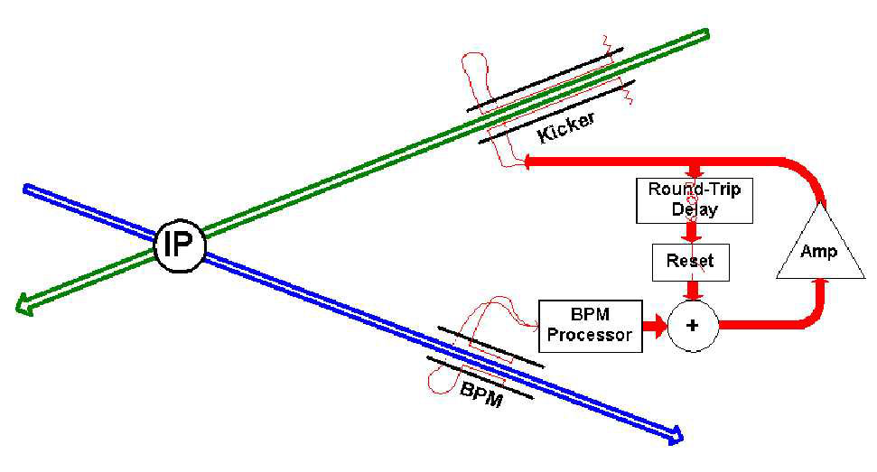
| Figure 3.3: Schematic diagram of the Steve Smith IP Fast Feedback System. The green arrow indicates the incoming beam and the blue arrow the outgoing beam, as seen by the IPFB system [60]. |
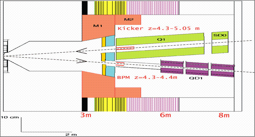
| Figure 3.4: Schematic diagram of a preferred location for the beam line components used in the Smith IPFB system within the suggested geometry of the NLC detector [52]. The scale is shown on the bottom left. |
A schematic diagram for the Smith design for the IP Fast Feedback system (herein abbreviated to IPFB) is shown in Fig. 3.3; the design consists of a number of discrete components:
The layout of the beam line components is shown in Fig. 3.4, within the suggested geometry of the linear collider detector (LC-D). A BPM is situated some 4 m away from the IP on the downstream side of one of the beams, with the intent of measuring the position of this beam as it flies away from the IP. Having done so, the measured position is converted into a voltage, by a series of filtering and normalising electronics, and passed to a power amplifier. This amplifier provides the signal for the kicker, situated in a similar position to the BPM but on the upstream side of the incoming beam. The kicker itself is intended to be an electrostatic parallel plate design (see [58] for full details), that steers the beam through a potential difference applied to the opposing plates (see Section 3.2.3).
The signal output of the BPM is not, on its own, in a suitable condition to be fed directly to the kicker in order to steer the beam by the required amount. A series of conditioning electronics converts the raw output of the BPM into a usable signal (see Section 3.3). The latency of the BPM processor is predicted to be less than 3 ns (see Section 3.3 and [58] for processor latency measurements). The last stage of these conditioning electronics is a variable attenuator, used to correctly normalise the BPM signal. Since the raw signal from the BPM (and the first stage of the BPM processor) is a function both of position and charge (see Section 4.1), one must divide out the charge information before passing the signal onto the kicker amplifier. A programmable attenuator is therefore used to divide by the charge in the bunch. The charge information can be measured at a number of different places throughout the whole accelerator, such as the damping rings; one would then have to ensure that this charge signal could be transmitted to the IP well in advance of the arriving bunch trains in order to program the attenuator in time. It would also be possible to average the charge from previous bunch trains, measured either by the IPFB BPM or one of the beam diagnostic systems situated within the damping rings or final focus.
In either case, the attenuator has the following operating conditions: it must be set (to 1/Q) before the beam arrives in order to correctly normalise each train, and it must take less time than the repetition rate of the machine (8.3 ms for the NLC, with
Having produced a normalised position signal in the above fashion, the signal is then passed, via a variable gain, to a kicker amplifier that drives the kicker itself. The use of a separate amplifier to drive the kicker, although at first glance adding to the latency of the system, avoids a number of impedance matching problems that would arise if one tried coupling the low power BPM processor electronics directly to the kicker (i.e. by amplifying the signal to the sufficient level to drive the kicker within the BPM electronics) [56]. The variable gain allows one to fine tune the corrective strength of the IPFB system as a whole: too weak a signal and the incoming beam is not steered close enough to the opposite beam; too strong a signal and the incoming beam is oversteered, causing the system to oscillate (see IPFB simulations in Section 3.4). The rise time of the kicker and amplifier is predicted to be the dominant factor in the system latency and is around 5 ns for the specifications given in [58].
Using a parallel plate approximation, the electric field E within the kicker, with gap width w, length L and a potential difference between the plates V, can be given as:
| (3.1) |
The force, F, on each particle with elementary charge q is:
| (3.2) |
Since
| (3.3) |
This implies that, for the NLC beam energy of 250 GeV, a kicker with a plate separation of 12 mm and length of 750 mm applies a beam deflection of ~0.25 nr/V. For a kicker located 4 m upstream of the IP and a relative vertical beam offset of 10 σy (where
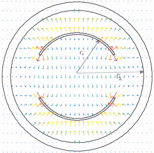
| Figure 3.5: Simulation of EM-field within a parallel plate kicker [60]. Note the uniformity and direction of the field at the centre of the kicker. |
However, simply steering the beam in response to a measured position does not in itself constitute a feedback system. With the system as currently described, the effect of the measurement and correction procedure would last only for as long as the latency of the whole system: the BPM would read a position offset on the outgoing beam, pass a (suitably scaled) signal to the kicker, which would then apply a corrective kick to the incoming beam. If the system were operating perfectly, the beams would collide directly head-on with one another, resulting in the outgoing beams experiencing no beam-beam deflection at the IP and setting the signal at the BPM to zero. As a result, after a single latency period the kicker would no longer be provided with an input, the beam would no longer be kicked and the system would be back to square one.
In order for an effective correction to be made to the train as a whole, a delay loop is introduced between the input of the kicker amplifier and the output of the BPM electronics, and is summed with the output of the normalised BPM signal. The purpose of the delay loop is to provide the feedback system with a (short-lived) memory: the length of the delay is set to equal the latency19 of the entire IPFB system. As such, once the BPM measures the result of the first correction to the bunch train i.e. sees the beam come back towards a head-on collision (by inference of the reduced beam-beam kick), therefore reducing the signal provided to the kicker, the delay loop acts to add in the previous BPM measurement, allowing the system to retain the correction that it had made previously. In this way, the corrective procedure becomes an iterative process, with smaller and smaller corrections being made to the incoming beam with each successive measurement (see Section 3.4 for simulations demonstrating this iterative procedure).
There are two possibilities for the signal to be used as the input to the delay loop: one can either use the input to the kicker amplifier or take the output of the amplifier and use an adjustable attenuator to drop the output voltage to the correct level. By choosing to take the output of the kicker amplifier, one compensates for any nonlinear behaviour on the part of the amplifier by recording (i.e. passing through the delay loop) the exact signal that was applied to the beam. However, using this signal can be disadvantageous, since a large droop on the amplifier output would go unnoticed by the system as a whole: the reduced kicker output and increased beam deflection (since the beam is no longer being steered directly into collision) would cancel one another out. Which choice of signal input holds the advantage is not yet clear [30].
Finally the IPFB system includes a reset for the delay loop. This reset is in the form of a gate or switch that controls the signal passing through the delay loop. The reason for such a gate is that, while there is no beam present, any noise inherent in the system will be amplified through repeated trips around the delay loop. The effect of this continuous signal addition is considerable, since the latency time
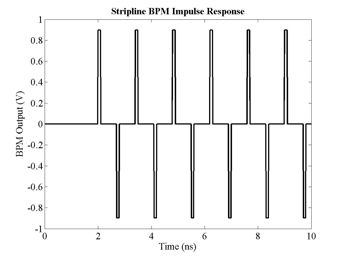
As stated earlier, the raw signal that the BPM produces is not in a state that is usable by the rest of the IPFB system. A full description of the response and signal output of a stripline BPM is given in Section 4.1.2; suffice it to say that the response of a stripline (such as the one proposed for use in the IPFB system) to a single bunch is approximately two delta functions, one the reflection of the other, as shown in Fig. 3.6. The initial signal is induced on the pickup as the beam passes the front of the stripline; the reflection comes from the free, unterminated end of the stripline. In order to get a sharp peak in frequency space corresponding to a bunched beam, one sets the stripline length at a quarter of the bunch spacing: for the NLC bunch spacing of 1.4 ns, this is 10.5 cm, assuming signals travelling at c (for more details see Section 4.1).
| Figure 3.6: The output of a single pickup in a stripline BPM in response to the first 6 bunches of a bunch train. The spacing of the initial spike and its reflection corresponds to twice the length of the strip, in this case 0.7 ns. |
The task of the BPM processor is to translate this signal of spikes into a recognisable approximation of beam position that can be passed to the kicker amplifier and used to drive the kicker. To transfer a waveform such as that seen in Fig. 3.6 directly to the kicker would not only be disastrous for any kicker amplifier that was attempting to charge and discharge a kicker with a such a pulse, but practically impossible from a timing point of view: the positive spike from the BPM signal — around 40 ps in length — must be aligned not only with its partner on the opposite strip for correct cancellation, but the resulting signal must also align with picosecond precision to the arrival of the incoming bunch. The usual tactic is to convert the signal into an approximately DC signal in a three stage process:
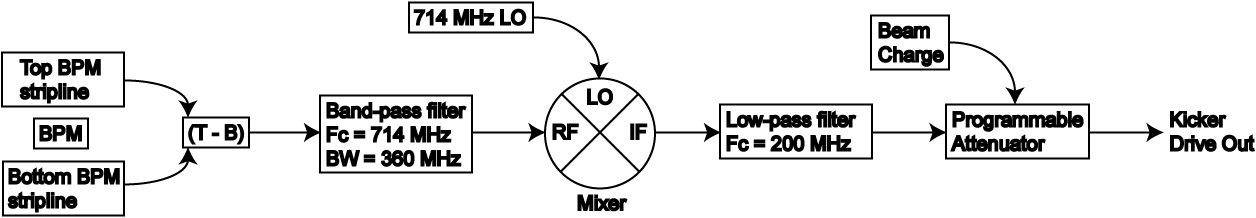
The commonly used phrase for this shift in frequency, in which the dominant high frequency components are replaced by a DC component through the use of a mixer (with a reference frequency equal to the input frequency) and a low-pass filter, is downmixing to baseband20. The block diagram for the BPM processor, using this filtering method, is shown in Fig. 3.7.
| Figure 3.7: Block diagram for the IPFB BPM processor; refer to the main text and [58] for full details. |
Even after this downmixing process, the signal would be of no use to the feedback system, since one cannot recover a position measurement from a single stripline. The usual method is to divide the difference of the signals on two opposing striplines by the sum of their signals: this processing scheme is called difference-over-sum, or Δ/Σ (see Section 4.1). In the case of a vertical beam position measurement y, using an upper stripline T and a lower stripline B, on opposite sides of the beam pipe to one another, the position is given by:
| (3.4) |
which gives an approximately linear response for a beam close to the centre of the BPM [61]. This method of difference over sum has the key property that any charge information is removed from the position measurement. Since the signal on a BPM stripline is a convolution of position and charge i.e. the output signal is a function both of the proximity of the bunch to the strip, and the number of charge carriers within the bunch, it is necessary to remove the charge information before making a position measurement. However, the disadvantage of doing such a calculation is that, while addition, subtraction and multiplication can be carried out at high speed with relatively simple electronic components, the same is not true of division [30]. As such, a programmable attenuator is used in the Smith IPFB system in place of the division in Eq. (3.4) to attenuate the signal by a factor of
If the difference over sum method is chosen for measuring beam position, it is possible to carry out the
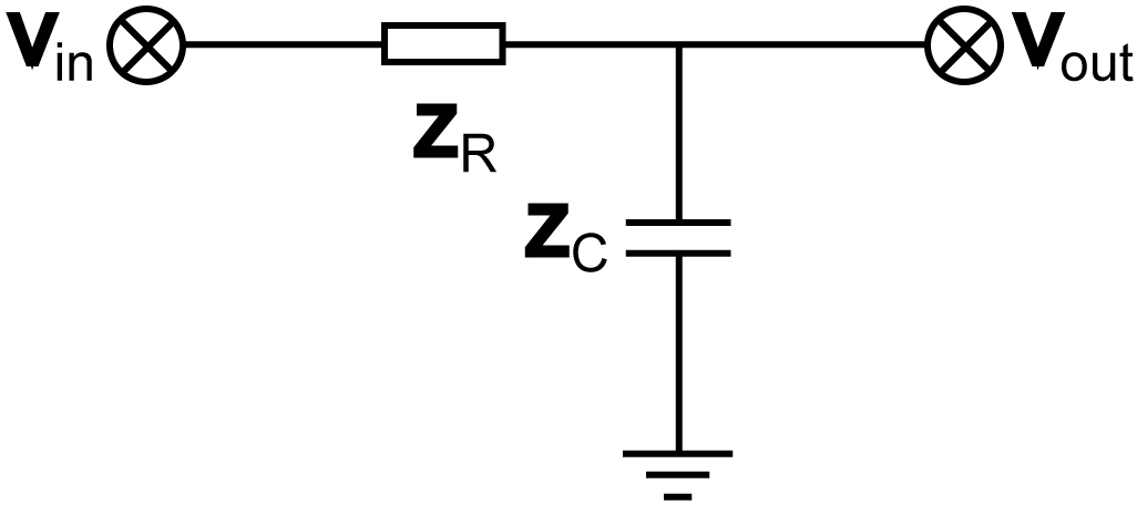
The first stage of the IPFB is a band-pass filter, used to convert the stripline signal (as shown in Fig. 3.6) into a more easily processable signal with a strong central frequency. All filtering of this nature (including the low-pass filter that constitutes the third processor component) essentially takes advantage of the frequency dependent impedance of a capacitor, whose impedance
| (3.5) |
where the angular frequency ω = 2πf and f is the frequency of the incoming signal. The output voltage Vout as a function of Vin is therefore the voltage drop across the resistor:
| (3.6) |
The amplitude (i.e. the real voltage, without consideration of the complex phase) of this equation is given by:
| (3.7) |
where Vout* is the complex conjugate of Vout. The ratio Vout/Vin is therefore:
| (3.8) |
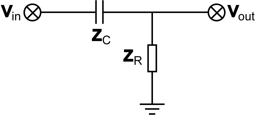
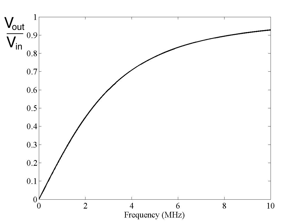
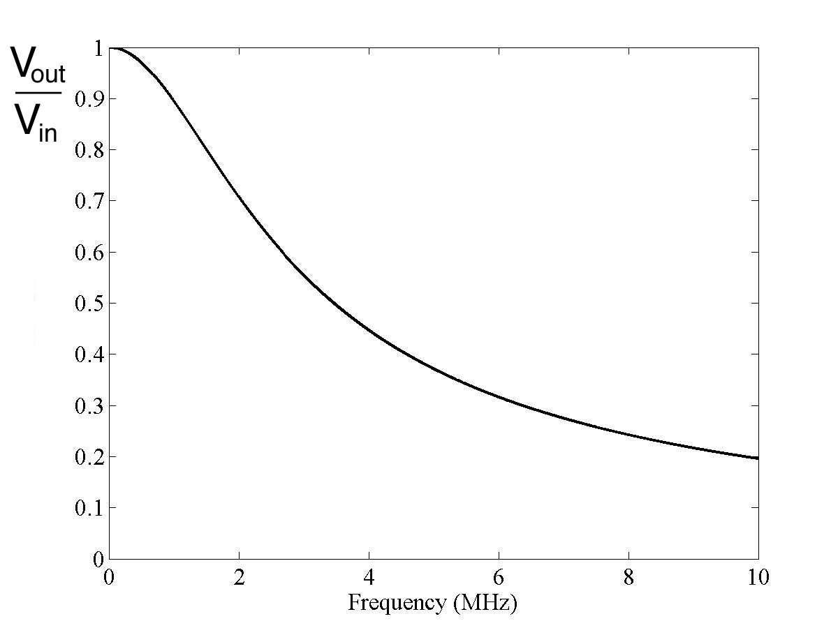
Eq. (3.8) gives the filtering characteristic of the simple circuit shown in Fig. 3.8(a); note that this filtering behaviour increases asymptotically towards Vout/Vin = 1. The frequency response of the circuit is shown in Fig. 3.8(b).
|
|
||||
| (a) Low-pass filter circuit | (b) Circuit frequency response | ||||
|
|||||
A similar argument follows for a low-pass filter: the circuit diagram is shown in Fig. 3.9(a). In this case, the current has the same form as Eq. (3.5), but on this occasion it is obtained by examining the voltage drop across the capacitor, giving:
| (3.9) |
Again taking the amplitude (by multiplying by Vout*), the ratio Vout/Vin is now:
| (3.10) |
In this case the frequency response now tends towards zero, as shown in Fig. 3.9(b). Note that at zero frequency (DC) all of the signal is passed without loss; at infinite frequency, all of the signal passes through the capacitor to ground. This is the opposite behaviour to the high-pass filter described above.
Having designed a filter to pass a certain frequency range, it is now possible to construct simple band-pass and band-reject filters with combinations of the above circuitry. A band-pass filter can be assembled with a low-pass and high-pass filter in series, ensuring that the frequency ranges overlap. A band-reject filter is the opposite: a low-pass and high-pass filter in parallel with very little frequency overlap. More complex filters exist that take advantage of the frequency characteristics of both capacitors and inductors [62]. For a band-pass filter this provides a sharper rolloff on either side of and flatter frequency response within the desired frequency range. One such band-pass filter is used in the first stage of the IPFB BPM processor: the Smith design uses a four-pole Bessel filter centred at 714 MHz, with a bandwidth of 360 MHz. A Bessel filter is chosen for its maximally flat time delay within the frequency range that it passes (the passband); the number of poles indicates the sharpness of the rolloff of the frequency response of the filter from passband to stopband (the frequency range rejected by the filter)21.
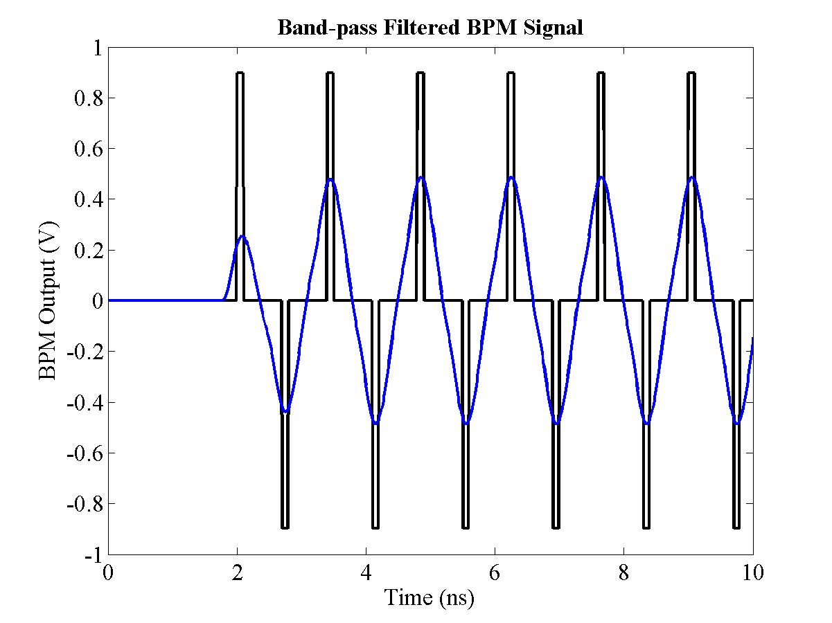
The purpose of this first stage filter is to convert the impulse response of the stripline to each bunch into a sine wave whose peaks maintain the magnitude information contained within the original pulses. Since the stripline BPM has a peak in frequency response at 714 MHz, and odd harmonics thereof, selecting a band-pass filter with a central frequency at 714 MHz ensures that all such information is maintained with the filtered signal. The reasons for choosing a relatively wide bandwidth of 360 MHz are twofold: firstly all higher harmonics are rejected, ensuring a clean signal, and secondly the larger bandwidth gives the filter a faster response, decreasing the rise time of this first stage [56]. The effect of the filter on the raw BPM signal is shown in Fig. 3.10.
| Figure 3.10: The output of a single BPM pickup after filtering with a band-pass filter centred at 714 MHz with a 360 MHz bandwidth. The raw signal is shown in black, with the filtered signal shown in blue. |
Having produced this modulated sine wave output, it is now necessary to convert this signal into an entirely positive (or negative, depending on the direction of deflection) signal in order to provide the kicker with a suitable signal for steering the beam. This is the job of the RF mixer, the second component of the IPFB BPM processor.
An RF mixer is essentially a device that, given two RF signal inputs, provides at its output a signal that is a linear combination of the sum and difference of the two input frequencies [62]. This is achieved by multiplying the two input signals, since the product of two frequencies, ω1 and ω2, gives the sum and difference frequencies:
| (3.11) |
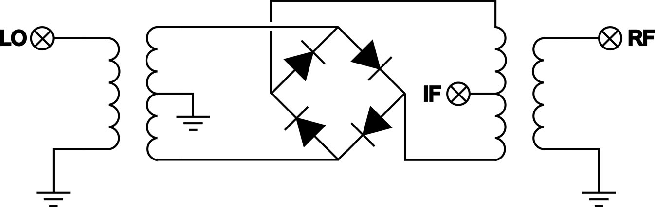
To make use of such multiplicative behaviour, a mixer must use devices that have nonlinear current-voltage relationships [63]: such a device is a Schottky-barrier diode, in which the current flowing through the device depends exponentially on the voltage, giving the required nonlinear behaviour (Schottky diodes are also chosen for their small forward voltage drop, increasing the efficiency of the circuit [64]). Most mixers are based on diode networks of some description [65]; the schematic diagram for a double-balanced diode-based mixer is shown in Fig. 3.11. A mixer has three ports: a RadioFrequency input (RF), a Local Oscillator input (LO) and an Intermediate Frequency output (IF)22. The source signal — in the case of the IPFB system, the band-pass filtered BPM signal — is input into the RF port. The LO port is used for the multiplying signal and is normally a single CW (continuous wave) frequency. The sum and difference frequencies resulting from the signal multiplication are output from the IF port.
| Figure 3.11: Circuit diagram for a double-balanced mixer featuring a standard 4 diode network (adapted from [66]). The LO and RF transformers provide improved isolation for each of the mixer ports. |
One can see how this is achieved using the mixer circuit diagram shown in Fig. 3.11. Using this diode arrangement, each diode is switched on in turn as it is driven by both the RF and LO signals23. The act of driving the RF and LO signals through the diode produces the desired multiplication (plus other intermodulation frequencies), resulting in the sum and difference signals appearing at the IF port.
Key to effective mixer operation is the removal of all unwanted intermodulation products. These are intermediate frequencies — such as
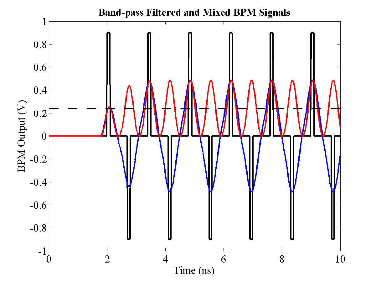
| Figure 3.12: The output of a single BPM pickup after filtering with a 714 MHz band-pass filter (blue) and mixing with a 714 MHz reference signal (red). Note that the mixed signal is twice the frequency but half the amplitude of the original band-pass filtered signal, with an additional DC offset (the dashed line indicates the DC offset). |
The effect of the mixer on the band-pass filtered signal can be seen in Fig. 3.12. The blue signal shows the band-pass filtered BPM signal as before; the red signal is the IF signal produced by the mixer. The mixer uses the filtered BPM signal (an amplitude-modulated 714 MHz signal as shown in Fig. 3.10) for its RF input; the LO signal is provided by the accelerator reference system and is a CW 714 MHz signal. The resulting IF signal is the superposition of the sum and difference signals following the multiplication rule in Eq. (3.11): a 1428 MHz sine wave, of half the amplitude of the original 714 MHz signal, added to a DC signal, again with half the amplitude.
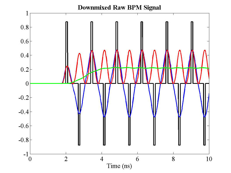
| Figure 3.13: The output of a single BPM pickup after downmixing to baseband. The raw signal (black) is band-pass filtered at 714 MHz (blue), mixed with a 714 MHz reference signal (red) and low-pass filtered at 200 MHz (green). These figures were generated using the simulation detailed in Section 3.4. |
The final stage in the IPFB BPM processor is to low-pass filter the signal. The filter specified in the Smith design is a four-pole low-pass Bessel filter, with a cutoff frequency at 200 MHz (see comments on active filters in Section 3.3.1). This removes the high frequency component — the sum signal, at 1428 MHz — leaving only the DC difference signal. Downmixing a signal to baseband is therefore just this process: mixing a signal with the correct LO frequency (i.e. a frequency very close to the RF signal) to produce a difference signal that is close to baseband (DC), then using a low-pass filter to remove the high frequency component. The resulting signal is shown in Fig. 3.13: the black, blue and red signals are as before, with the resulting downmixed signal shown in green. Close inspection of this signal shows a very slight 1428 MHz modulation present superimposed upon the downmixed BPM signal. The BPM signal that results from this three stage processor is now a DC signal that is proportional to both position and charge. It is now in suitable condition to be passed to the programmable attenuator for the final stage of processing (removal of charge information) before being used to drive the kicker amplifier.
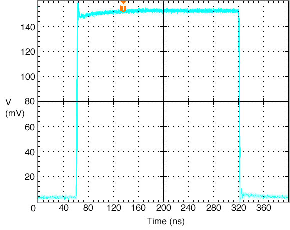
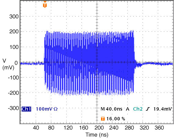
Using the components specified in the Smith IPFB design and the previous section, bench tests were carried out, with Steve Smith, on the BPM processor [67]. It was not possible within these tests to truly simulate the response of a stripline BPM (Fig. 3.6). A sine wave generator was therefore used to simulate the band-pass filtered BPM signal at 714 MHz, in an attempt to replicate the signal shown in Fig. 3.10. The filtered BPM signal is approximately a 266 ns long RF burst (replicating the true NLC bunch length of 266 ns) at 714 MHz, with an appropriate rise and fall time of approximately 3 ns (simulating the response time of the band-pass filter).
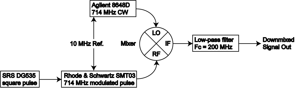
| Figure 3.14: Block diagram for the IPFB BPM processor tests, showing the various signal paths used to simulate the BPM bunch train signal. |
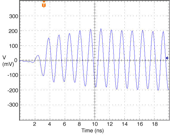
The block diagram for the BPM processor tests is shown in Fig. 3.14. Three signal generators were used to simulate this bunch train signal. An Agilent 8648D synthesized signal generator was used to produce the 714 MHz CW output for the mixer LO input. A Rhode & Schwartz SMT03 signal generator was used to simulate the actual band pass filtered BPM signal i.e. the mock bunch train signal, using a modulated 266 ns 714 MHz pulse (Fig. 3.15(b)). This square pulse modulation for the SMT03 was provided by an SRS DG535 square pulse generator (Fig. 3.15(a)). The DG535 square pulse also had a measured rise time of ~3 ns, providing the necessary rise and fall time for the RF signal from the SMT03 (Fig. 3.15(c)). The SMT03 was phase locked to the 8648D with a 10 MHz reference pulse. The phase locking of these 2 units was not exact, leading to a certain amount of jitter on the resultant mixer IF output. The bunch train produced by the SMT03 was used as the mixer RF input.
|
|
||||
| (a) Low-pass filter circuit | (b) Circuit frequency response | ||||
 |
|||||
|
|||||
|
|||||
 |
|||||
|
|||||
|
|
||||
|
|
||||
|
|||||
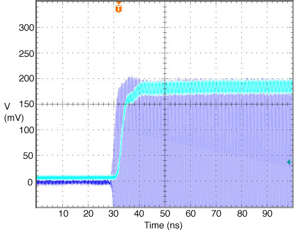
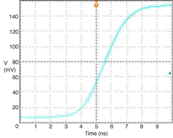
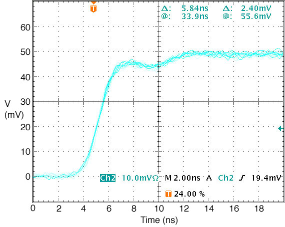
Two Mini-Circuits mixers were used for the test: a low power ZFM-2000 (requiring a +7 dBm LO input with a max. RF input of +1 dBm) and a high power ZP-5MH (+13 dBm LO, +9 dBm max. RF). The higher power mixer was predicted to have a faster rise time. For both mixer tests, a Mini-Circuits SBLP-200 low-pass filter, with a cutoff frequency of 200 MHz, made up the third processor stage. The response of the two mixers is shown in Fig. 3.16. The first obvious feature to note is that both processors replicate the bunch train signal, performing exactly as predicted by the simulation shown in Fig. 3.13. The rise times of the two mixers are also different: the 10-90% time for the high power mixer (Fig. 3.16(c)) is around a nanosecond faster, at 2 ns, than the low power mixer (Fig. 3.16(b)), with each using the same low-pass filter on the IF output. The delay time between input and output was the same for both mixers at ~2 ns.
However, the output of the high power mixer is not as smooth as that of the low power version: there is an extra artifact that appears on the leading edge of the pulse (Fig. 3.16(c)) that is not present on either the original pulse (the blue trace in Fig. 3.16(a)) or the low power mixer output. The signal oscillation that appears on the two traces in Fig. 3.16(a) is not a feature of the processor circuit but a result of crosstalk between the SMT03 pulse generator and the oscilloscope inputs used to record the signals (cf. Fig. 3.16(b)). The timing jitter that appears on the pulses is due to the lack of phase reference between the DG535 square wave generator and the SMT03.
In summary, the lower power mixer (ZFM-2000) is recommended for use in the IPFB BPM processor. It is on the order of 1 ns slower to rise than the ZP-5MH, but has a cleaner frequency response, showing no leading edge ripple (which appears with the ZP-5MH) while still replicating the envelope of the BPM signal. It has the added advantage of being cheaper.
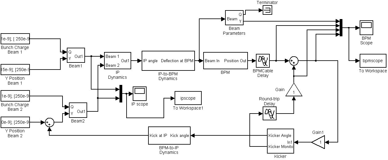
As proof of the corrective capability of the IPFB system, extensive simulations have been carried out independently by Steve Smith [58] and Glen White [68]. The IPFB system was modelled in the Matlab subsidiary package Simulink, allowing accurate simulation of each of the electronic components utilised. The Simulink block diagram for the simulation is shown in Fig. 3.17. Included in the simulation were the various system transport delays (beam flight times and electronic component signal delays), basic modelling of the beam-beam interaction, the stripline BPM response to a bunched beam and the fill time and signal response of the kicker. Fig. 3.13 shows the simulated response of the BPM and the BPM processor in Simulink to a bunched beam at 714 MHz.
| Figure 3.17: Block diagram for Simulink simulation of IPFB system. A number of simulated components, such as the BPM processor, are contained within sub-blocks and are therefore not shown. |
|
||||||||||||||||||||
|
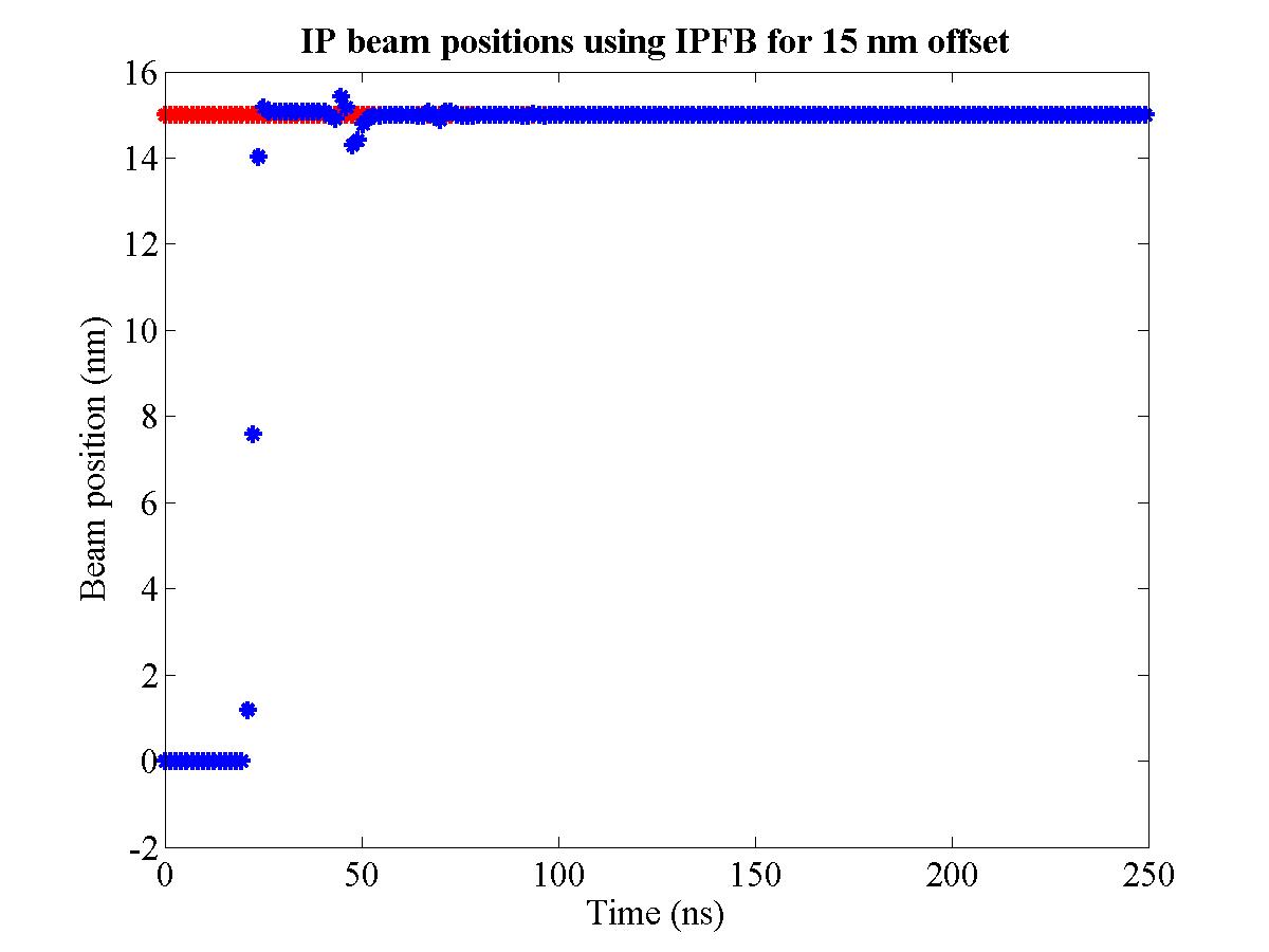
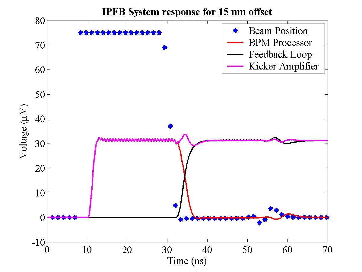
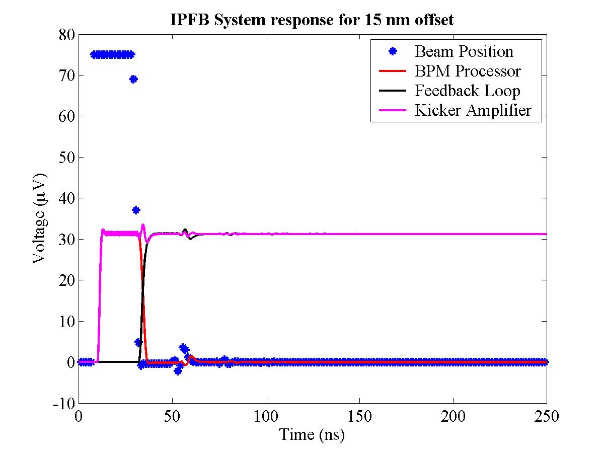
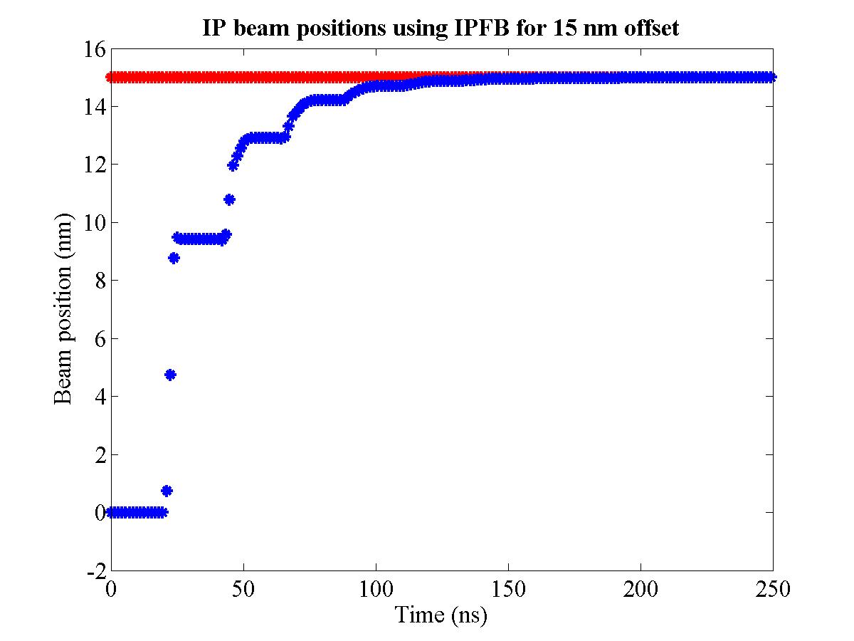
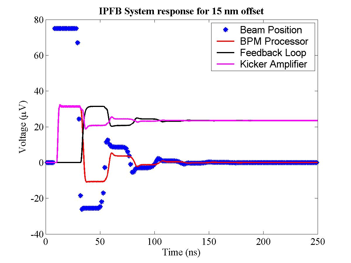
| Figure 3.18: Simulated beam position at the IP using corrective intra-pulse fast feedback for an initial offset of 15 nm (~5σy) and kicker gain 2.4×10⁻⁴. |
The simulation was initially set up with a relative beam offset of 15 nm: this is ~5σy. The initial parameters are summarised in Table 3.124. Three different kicker gains were used to measure the gain dependence of the IPFB system. The simulated effect of the IPFB system with a 15 nm beam offset is shown in Fig. 3.18. After a single round trip the IPFB system has corrected the lower beam (blue) and steered it towards the higher beam (red), bringing the two back into collision. After another latency period the IPFB system makes a further correction: this occurs at ~55 ns. The ripple that occurs in the beam position at this point is a result of the delay loop signal rising as the BPM output falls: this can be seen more clearly in Fig. 3.19.
|
|
||||
| (a) IPFB system response — first 70~ns | (b) IPFB system response — full train | ||||
|
|||||
The signal levels within the IPFB system for the first 70 ns of the train are shown in Fig. 3.19(a); the full train is shown in Fig. 3.19(b). As the beam reaches the IPFB BPM, a corresponding offset is measured in the BPM after 8 ns (blue signal). This beam signal is downmixed to baseband by the BPM processor which shows a corresponding rise at 10 ns (red signal). This signal is fed into the kicker amplifier, which initially tracks the BPM processor signal (magenta signal). After a single latency period of ~22 ns, the incoming beam has been corrected almost perfectly, leaving only a small beam-beam offset and resulting deflection, meaning that only a small signal is now registered at the IPFB BPM after 35 ns. At this point, the signal from the delay loop arrives (black), compensating for the falling BPM signal and keeping the kicker amplifier output at the correct level. The small residual signal from the BPM makes a small correction to the signal from the delay loop, adjusting the beam position with a small correction. The whole process then repeats, with a smaller correction applied from the BPM signal on each successive pass around the delay loop: the small wrinkle in the delay loop signal can be seen at 57 ns, with a corresponding deviation in the kicker signal. Once the incoming beam has been steered to such an extent that the beams are colliding head-on, the BPM processor will no longer produce a position signal, leaving the correct signal now running round the delay loop and being output into the kicker: this can be seen at ~70 ns.
|
|
||||
| (a) IP beam position | (b) IPFB system response | ||||
|
|||||
|
|
||||
| (a) IP beam position | (b) IPFB system response | ||||
|
|||||
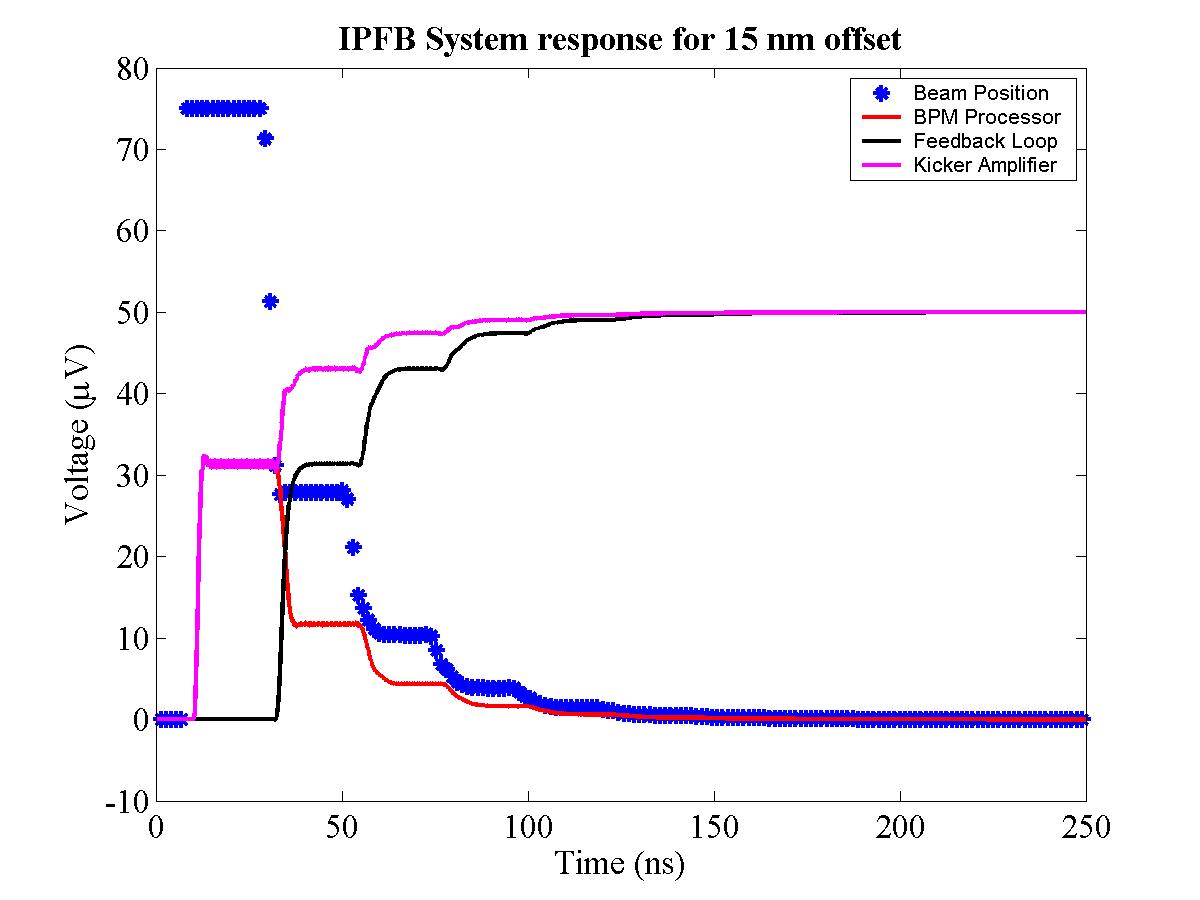
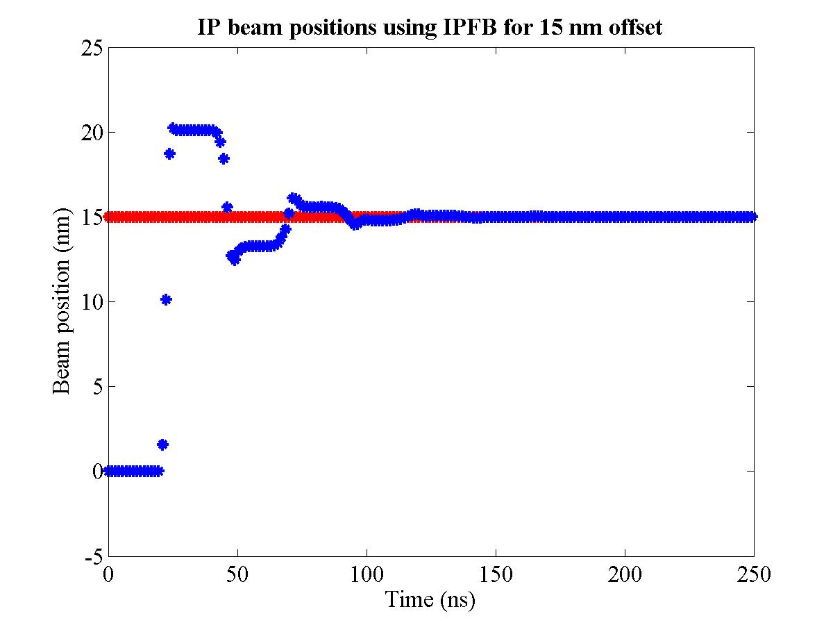
Two other simulations, with different kicker gains are shown in Figs. 3.20 and 3.21. Within the simulation there are a number of different gains that control the relative signal levels of each of the different parts of the electronics. One of these gains controls the signal strength that is output by the kicker amplifier to drive the kicker. Setting this gain too low causes the IPFB system to undercorrect the incoming beam, meaning that a further significant correction has to be applied. In this scenario (Fig. 3.20) the system takes longer to close the delay loop, resulting in a less rapid luminosity recovery. Fig. 3.20(b) shows this clearly: instead of coming close to zero with a first pass around the loop at 35 ns, the correction is not large enough, meaning that the system needs several passes before the beam is properly corrected.
On the other hand, setting the kicker gain too high also results in a longer time to recover a head-on collision, but for the opposite reason (Fig. 3.21). The overly strong correction causes the incoming beam to overshoot, missing its intended target. The IPFB system has to make a negative correction and steer the beam in the opposite direction (or, more accurately, less far in the same direction), resulting in the system going into oscillation. Fig. 3.21(b) shows this signal oscillation: at 35 ns the BPM processor signal overshoots beyond zero, since the beam has been overcorrected, and the successive passes around the loop repeat this behaviour. Since the gain is set only slightly too high, this oscillation damps out with successive passes around the delay loop; however, for very high gain settings, the system can oscillate continuously and even make the situation worse, as the beam is steered further and further from a head-on collision with each successive correction.
|
|
||||
|
|||||
The simulations detailed above are incomplete, however, since only a linear model is used for the beam-beam interaction (linear relationship between beam-beam offset and kick strength). Detailed examinations of the effect of the IPFB feedback gain have been carried out by Glen White, using GUINEA-PIG to accurately model the effects of the beam-beam interaction [68]. The effect of the IPFB system on the luminosity of the NLC for different feedback gains is shown in Fig. 3.22. These simulations demonstrate the effectiveness of the IPFB system in correcting a relative beam-beam offset and the ability of the system to correct such an offset well within a single bunch train.
More detailed simulations, also undertaken by Glen White, indicate that for random (Gaussian) noise on the bunch position within a train, the IPFB system does not improve the luminosity [68]. In fact, for random bunch-to-bunch jitter, the feedback system actually makes the situation worse. However, given the sources of such beam jitter, the evidence presented by these simulations indicates that the IPFB system makes a valuable correction to the relative offset between the two bunch trains and recovers a significant amount of luminosity that other feedback systems are unable to correct for (see Section 3.1).
| Figure 3.23: Overhead view of the SLAC Linear Collider, showing the location of the linac, damping rings, electron and positron storage rings and the various experiments [69]. Sector 2 is the section of the linac between the entry and exit points of the damping rings on the left of the picture. |
Having demonstrated the intended IPFB system operation and its effect in luminosity recovery, a full system beamline test was proposed. Such a test was deemed necessary in order to measure the behaviour of the IPFB system in areas that the simulation was unable to accurately model, such as the interaction of the beamline components with the beam itself. Two possible locations for such a test were suggested: Sector 2 of the SLAC SLC accelerator and an unused region of the test accelerator for the Next Linear Collider, the NLCTA (also based at SLAC).
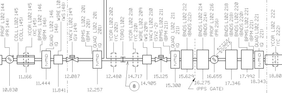
An overhead view of the SLC is shown in Fig. 3.23. The section of the accelerator that was originally considered for use by an IPFB beam test is Sector 2, towards the front end of the linac. The start of Sector 2 encompasses the region of the linac either side of the Damping Rings, referred to as the Damping Ring Injection Point (DRIP). A blow-up of 12 m of the first section of the linac at Sector 2 is shown in Fig. 3.24. The DRIP covers approximately the first 8 m of Sector 2, up to the start of the schematic. The region downstream of the DRIP — the ASSET (Accelerator Structure SETup) region — is currently occupied by the Collimator Wakefield experiment (for details, see [70] and related material, such as [71]).
|
|||||||||||||||||||||||||||||||||
| |||||||||||||||||||||||||||||||||
| Figure 3.24: Blow-up of 12 metres of the first section of Sector 2 of the SLAC linac. The DRIP finishes approximately at the start of the schematic. The wakefield region is between the two collimators at 8.06 m and 11.17 m; the ASSET chicane is downstream of the wakefield box, between the two vacuum valves at 12.09 m and 15.13 m and is marked ‘8’. Measurements are in metres (adapted from [73]). |
The beam parameters for the SLC in the region of Sector 2 are summarised in Table 3.2. The fixed target experiments (based historically within both SLAC End Stations, but now housed only within End Station A) make use of very different beams to that of the colliding beam experiments (such as BaBar and SLD): the current fixed-target experiment is E158. In an experiment designed to measure the electro-weak mixing angle through Møller scattering, E158 will direct a beam of longitudinally polarised electrons onto a hydrogen target housed within End Station A (see [74] for full details). To maximise the event rate, the electron beam is initially intended to be a 100 ns CW beam of 6×10⁸ particles per bunch, rising to a 300 ns long beam for a second series of data runs. An IPFB beam test would make use of the short bunch spacing (0.35 ns) and NLC-like train length (100-300 ns) to simulate the conditions that exist for the real IPFB system. It was also suggested that a subharmonic buncher could be used within the SLC injector with a bunching frequency 1/16th of the standard bunching frequency (2856 MHz), giving a 5.6 ns bunch spacing [72].
The intention was to install a series of fast kickers into the ASSET region of Sector 2 around the wakefield box used for the collimator wakefield experiments. A first magnet would steer the beam off-centre, simulating a beam-beam kick. This position offset would then be registered by one of the existing BPM's within Sector 2, which would be commandeered for the use of this beam test. Upon measuring the beam position, an appropriately-modified25 version of the real IPFB system would process the beam signal and feed it back upstream to a second corrective magnet, such as the parallel plate kicker described in Section 3.2.3. The iterative process of correction would then continue as with the true IPFB system, by setting the normalised signal coming from the BPM to zero.
However, a number of problems became apparent with trying to install an IPFB test setup within Sector 2. Firstly, the schedule for installation within the linac would allow access only once every few months. Given this severe limitation on the number of allowed accesses, it was also unclear where the electronics and data acquisition systems would reside. Any failure, fabrication error or design oversight of the feedback electronics would require a delay of up to 6 months before it could be removed or modified, if it were to sit in the accelerator tunnel. However, placing the electronics outside the tunnel in the klystron gallery26 was unacceptable from a system latency point of view. The best alternative that was presented was to keep as much of the system in the tunnel, while running cables up to a DAQ system in the klystron gallery.
In addition to this, it quickly became apparent that the BPM's and associated electronics installed in Sector 2 were not up to the task required of them by an IPFB beam test. While having a position resolution of a few microns, the minimum time resolution was only on the order of 50 ns [56], not suitable even for the subharmonic buncher spacing of 5.6 ns, and certainly undesirable for a fast feedback system intended to work on nanosecond timescales. Finally, there were the numerous associated problems of running parasitically with and to the schedule of another experiment (E158), with no control over beam conditions or running time. As such, an alternative location was used: the NLCTA.
The Next Linear Collider Test Accelerator (NLCTA) was originally designed to test a complete unit of the NLC RF system i.e. the accelerating structures and RF production, distribution and delivery systems that will be used in the NLC [75]. Although the control and timing systems are intrinsically linked with those of the main accelerator, the NLCTA is otherwise entirely independent of the SLC, with its own injector, accelerating structures and beam dump. An overhead view of the NLCTA is shown in Fig. 3.25. There are six sections of the accelerator that are set aside for accelerating structures: only the first four of these are currently in use for structure tests. This gave the possibility of using the last two unused drift spaces for an IPFB beam test.
Since such a beam test would be designed to test the nanosecond-scale response of the feedback electronics for the IPFB system, the experiment was christened FONT: Feedback On Nanosecond Timescales27.
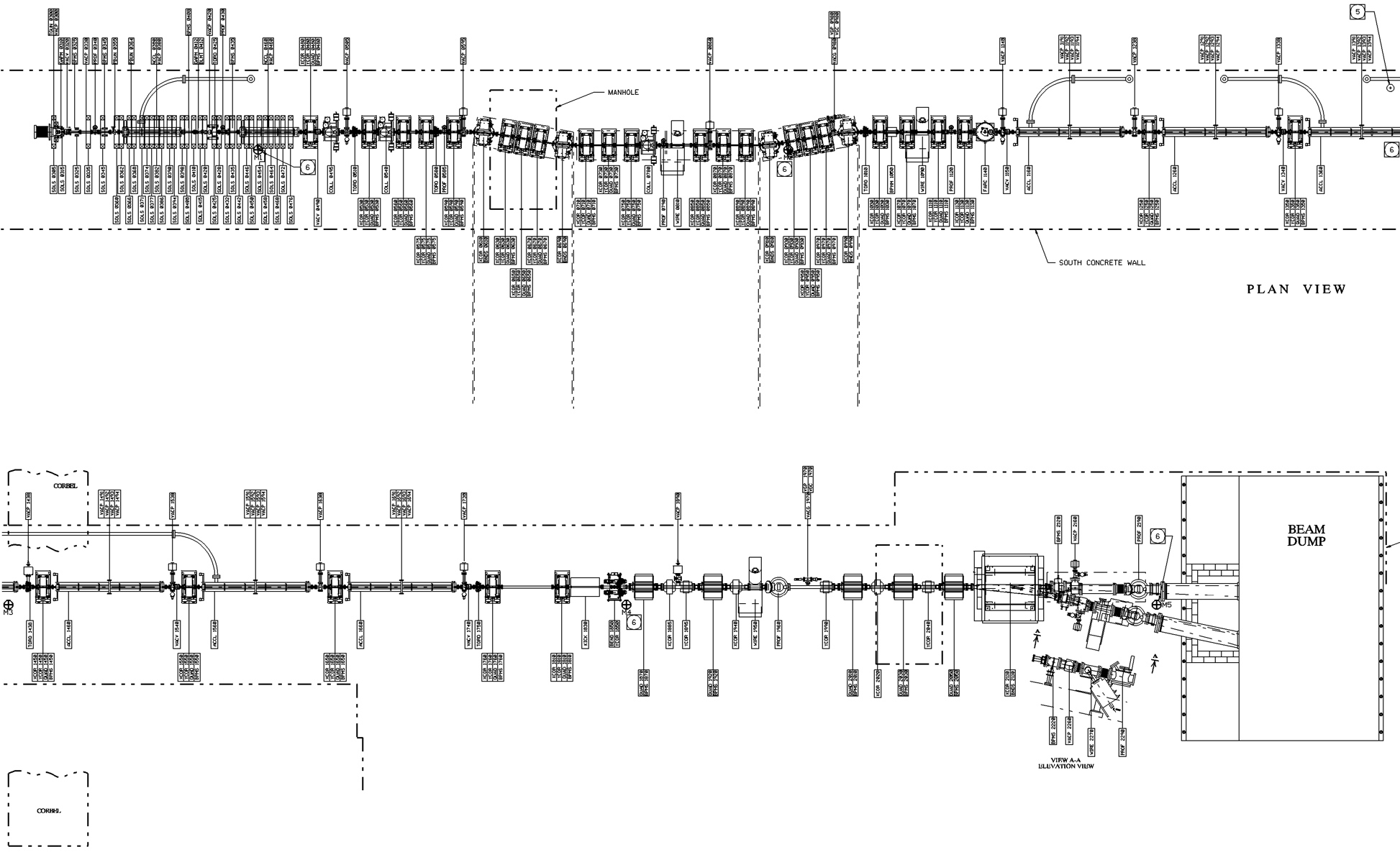
| Figure 3.25: Ground Plan of the NLCTA. The gun, injector and chicane are located at the front end of the accelerator (left), with the spectrometer, beam dump and the majority of the structures on the rear half (right). See also Figs. 5.1 and 5.2; figure adapted from [76]. |
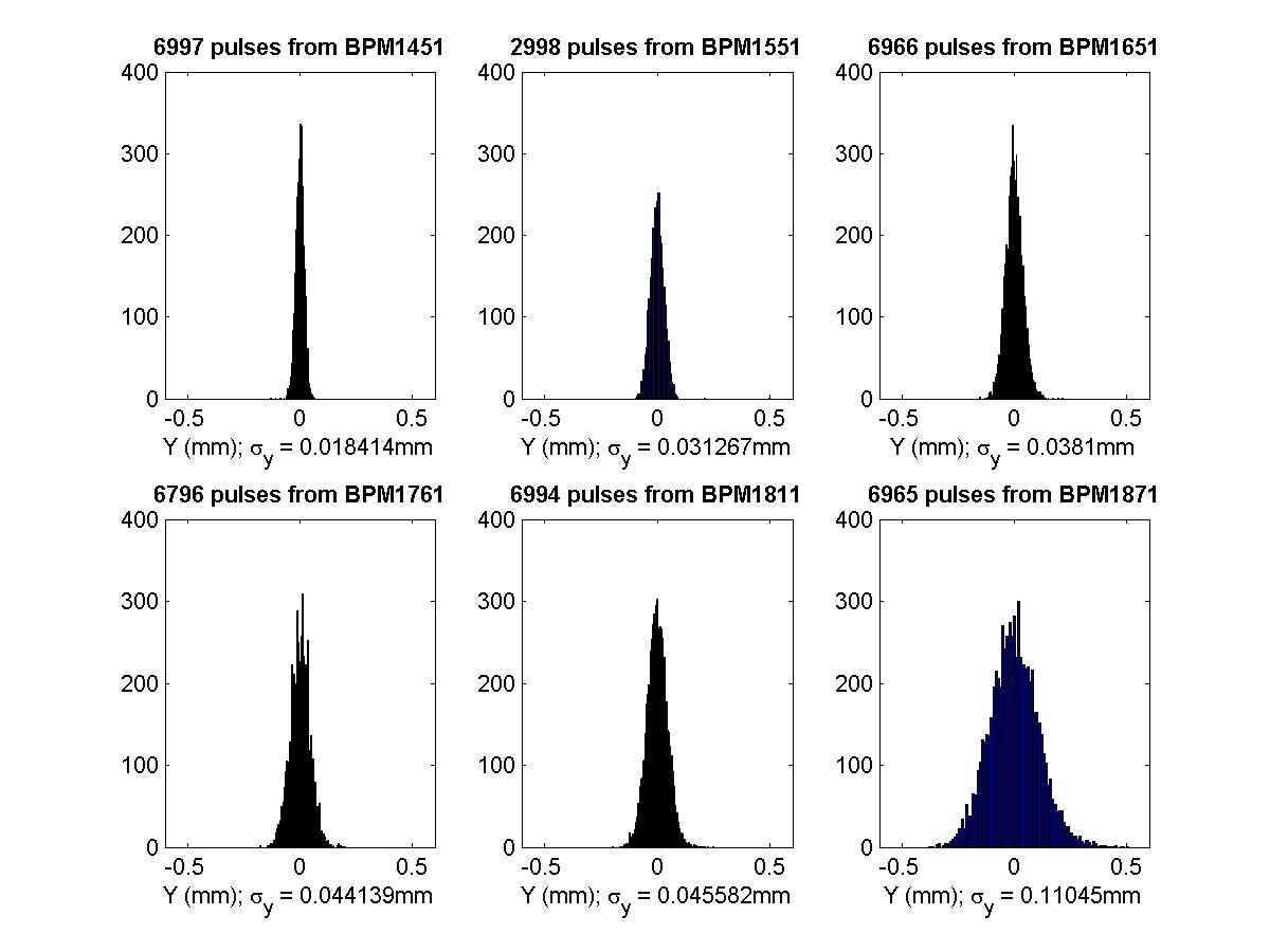
| Figure 3.26: NLCTA pulse-to-pulse beam jitter measurements, taken with the six consecutive striplines situated downstream of the test structures (see Fig. 3.25): the FONT BPM is installed upstream of BPM1761 (see Fig. 4.8). |
|
|||||||||||||||||||||||||||||||||
| |||||||||||||||||||||||||||||||||
The beam parameters, as summarised in Table 3.3, provided a separate challenge for the purposes of a FONT beam test. Although the beam energy is lower28 by more than an order of magnitude than that in Sector 2, the much larger spot size and beam jitter would mean that a comparatively larger kicker voltage would be required in order to kick the beam a measurable amount. The minimum kick required for a measurable beam offset must steer the beam at least as far as the r.m.s. position jitter on the beam [30], meaning that an NLCTA-based FONT system would still have to kick the beam half the distance of one on Sector 229, giving half the kicker voltage and a quarter of the power. As part of the preliminary measurements for FONT, the beam jitter on the NLCTA was measured using the NLCTA striplines: these measurements are shown in Fig. 3.26.
More importantly, the beam used at the NLCTA does not make use of any subharmonic bunching system, meaning that the electrons are injected continuously, resulting in a CW beam bunched at the structure frequency of 11.424 GHz. Thus the same problem of finding a BPM suitable for use at Sector 2 exist to an even greater extent on the NLCTA. A full description of the BPM that was constructed to measure beam position at the NLCTA is given in Chapter 4. In spite of these problems, it was felt that the obvious advantages of using the NLCTA over the main linac were enough to sway the argument in favour of constructing the FONT experiment on the NLCTA. These advantages were:
This is all, of course, within the operating constraints of the NLCTA. Although running beam was not necessary for the structure tests, since the main activity of the NLCTA was RF processing of the structures, it would not be possible to select arbitrarily the operating conditions of FONT. FONT would still be playing second fiddle to the main purpose of the NLCTA — to develop high gradient RF structures for the NLC — but the interference between the two experiments was intended to be minimal. The design, construction and results of the FONT experiment are given in Chapter 5.
19 The latency of the system is defined as the combined flight time of the incoming beam to the kicker and the outgoing beam to the BPM, plus the signal propagation delay through the IPFB electronics. In other words, the time it takes for the BPM to measure an offset, pass a signal to the kicker, have the kicker correct the beam and finally see the results of this correction. This is predicted to be on the order of 30 ns for the real system: 2×12 ns time-of-flight from IP to the IPFB system (situated ~4 m from the IP), plus 6 ns processing time [58].
20 Baseband is the frequency space enthusiast's term for a signal that tends towards DC, or a signal with a dominant component at zero Hertz.
21 Other such active filters include the Chebyshev (fast rolloff from passband to stopband) and Butterworth (maximum flatness of frequency within the passband) [62].
22 When driven as a modulator i.e. when upconverting a signal to a high frequency and making use of the
23 Other mixer types include single-balanced — consisting of a pair of diodes — and single-ended, with just a single diode. As the mixer layout increases in complexity, there is a corresponding improvement in port isolation and reduction in intermodulation products [63].
24 An IP-BPM flight time of 6.6 ns corresponds to the IPFB system being ~2 m downstream of the IP. This is unlikely to be the true location, since it places the IPFB system well within the detector; however, it does not affect the principle of operation of the system.
25 Appropriately-modified in this context means that the filter frequencies would have to be correctly tuned for the E158 bunch spacing i.e. 2856 MHz. The LO input for the mixer would therefore also be set to 2856 MHz.
26 The klystron gallery is the building that sits directly above the accelerator tunnel, above ground, and houses the klystrons that power the linac accelerating structures.
27 © Glen White, 2001.
28 The given beam energy is for an unaccelerated beam, in which only the pre-accelerator that resides upstream of the chicane is used to power the beam, rather than any of the test structures downstream of the chicane.
29
© Simon Jolly 2003