As described in Section 3.5, an experimental test of the IP fast feedback system was considered crucial in proving the principle of a feedback system with a nanosecond scale time response. Although both the IPFB simulations (Section 3.4) and the bench tests of the BPM processor components (Section 3.3.3) give some degree of confidence that the true IPFB system should behave as predicted (see Section 3.2 and [58]), it was felt that a true experimental test of the electronics, incorporating some normalisation scheme (nominally the Δ/Σ scheme as used for the X-band BPM, as described in Section 4.6), and a method of high speed position correction of a real bunched beam was essential in demonstrating the effectiveness of the IPFB system. Such a test, given the name FONT (Feedback On Nanosecond Timescales), was realised on the NLCTA, as mentioned briefly in Section 3.5.2. The aim of the FONT experiment was to replicate the conditions of the NLC IP to allow a comprehensive test of the IPFB electronics.
A series of electronics was designed and constructed at SLAC and Oxford with this intention in mind. The key principle behind FONT was to be able to apply an iterative correction to an off-centre beam within a single bunch train. A number of options were considered for the main objective of the FONT experiment. However, that which was felt to most closely replicate the goals of the IPFB system was to centre the beam at a single BPM. In other words, a beam would be seen to be off-centre by a BPM and, through re-steering that beam based upon the measurement made by the BPM, set the BPM signal to zero. This is clearly not the same as steering a beam to a desired trajectory, as is the requirement for the real IPFB system. With just a single BPM, the FONT system has no knowledge of the angle, and hence the trajectory, since only a single position measurement can be made. However, this is essentially the same as the current design of the IPFB system: its only knowledge of its success is whether, as a result of the beam-beam interaction, the position at the BPM is set to zero. As such, it was felt that designing the electronics to this end would provide the best proof of principle of the IPFB system electronics.
The obvious disadvantage of using the NLCTA for a beam test of the IPFB system is that the accelerator has no IP. The feature that sets the IPFB system apart from other feedback systems is its use of the enormous beam-beam kick between the two colliding bunches to translate a nanometre-level offset at the IP into a micron-level position measurement at the IPFB BPM. Unfortunately, it is the beam-beam interaction that is the least well-known element of the entire IPFB system. However, since no nanometre colliding beam facilities exist on which one could build a test setup of the IPFB system, one is limited to using a single beam and modifying the experimental setup accordingly. The layout of the FONT experiment at the NLCTA and the replication of the beam-beam interaction are dealt with in Sections 5.1.1 and 5.1.2.
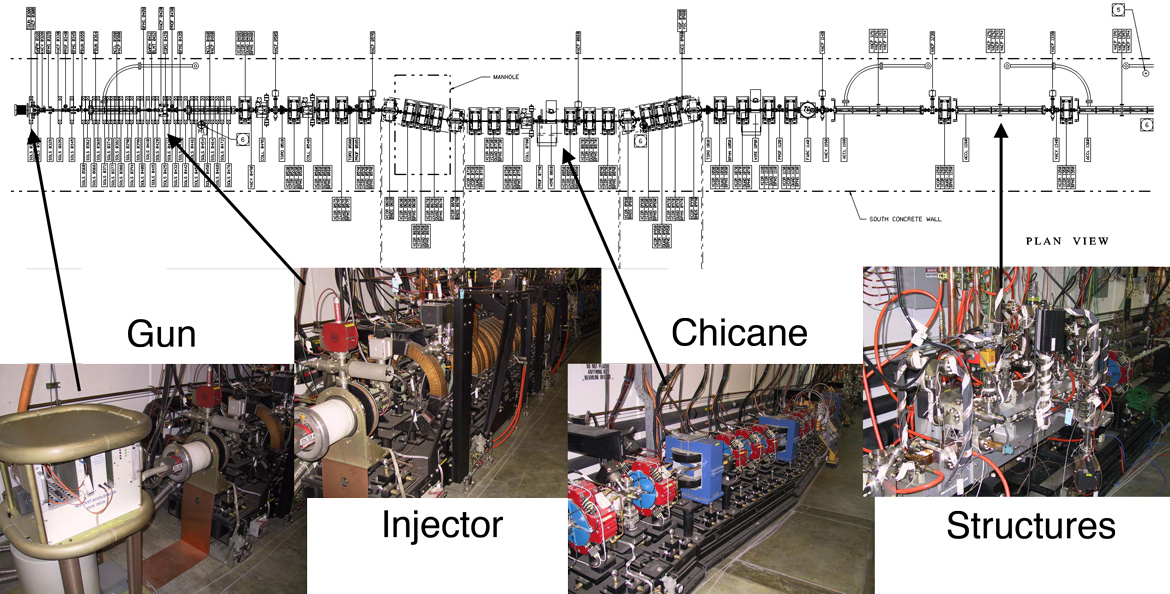
| Figure 5.1: The front section of the NLCTA, showing the gun, injector, chicane and one of the test structures. Figure adapted from [76]. |
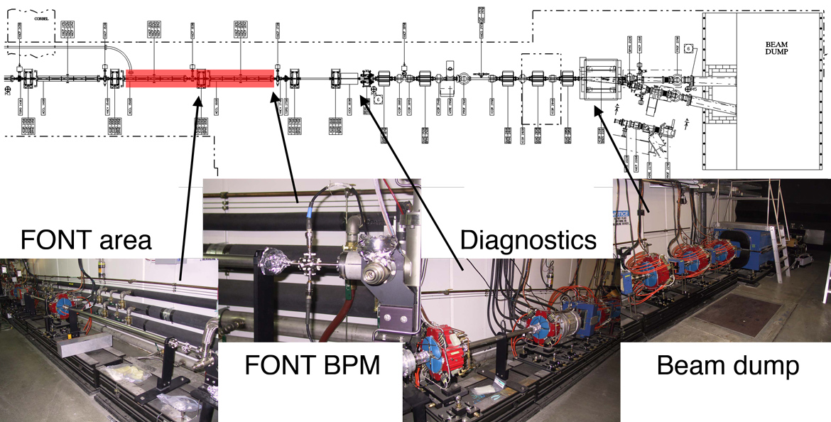
| Figure 5.2: The rear section of the NLCTA, showing the diagnostic tools, the beam dump and the area used for the FONT experiment. The diagnostics include a toroid, a profile monitor and a large kicker used to measure the longitudinal beam profile and beam energy. The FONT area is marked in red, between quads QD1550 and QD1760. The FONT BPM is located at the downstream end, upstream of QD1760 and Toroid 1750. Figure adapted from [76]. |
The principle behind the FONT experiment was to try and make a rapid correction to a beam offset as measured by the FONT BPM. The offset would be introduced upstream of the BPM with a dipole and be measured by the FONT BPM. The signal from the BPM would then proceed through the IPFB electronics in the same way as the actual system (see Section 3.2.1). The raw BPM signal is processed using the Δ/Σ method; a high speed power amplifier is then used to drive a kicker to correct the measured beam offset. In this way, the FONT experiment would replicate the whole IPFB system. An important consideration when choosing the location of FONT on the NLCTA was the anticipated latency of the system. It was crucial to be able to match the round trip delay of FONT with that of the real IPFB system: this is the reason for FONT taking up some 4 m of the NLCTA beamline. The total beam flight distance, for the IPFB system in its current location (see Fig. 3.3), is some 8 m, with only a few centimetres of cable length used to connect the BPM processor to the kicker amplifier. For FONT, using 4 m of beamline gives the same round trip distance, since the processed BPM signal must be transmitted back upstream to the start of the FONT region where the beam offset and correction would be applied.
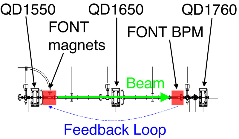
| Figure 5.3: Schematic diagram of the FONT region of the NLCTA, showing the various beamline components. A description of the FONT BPM is given in Chapter 4; the FONT magnet assembly is detailed in Section 5.2. Figure adapted from [76]. |
Changing the length of the beamline used for FONT would also change the requirements of the FONT electronics. Moving the BPM closer to the source of the beam offset would shorten the latency period, allowing greater scrutiny of the feedback electronics by increasing the number of latency periods for which FONT would operate. However, for the same angular deflection applied to the beam the BPM would register a smaller signal, requiring a larger gain in, and increasing the power requirements of, the kicker amplifier. Increasing the length of beamline used for FONT would have the opposite effect, decreasing the required kick while increasing the latency period. As such, a beam flight distance of 4 m was also considered optimum for the FONT electronics. There were also beam optics considerations in the location of FONT, which are detailed in the next section.
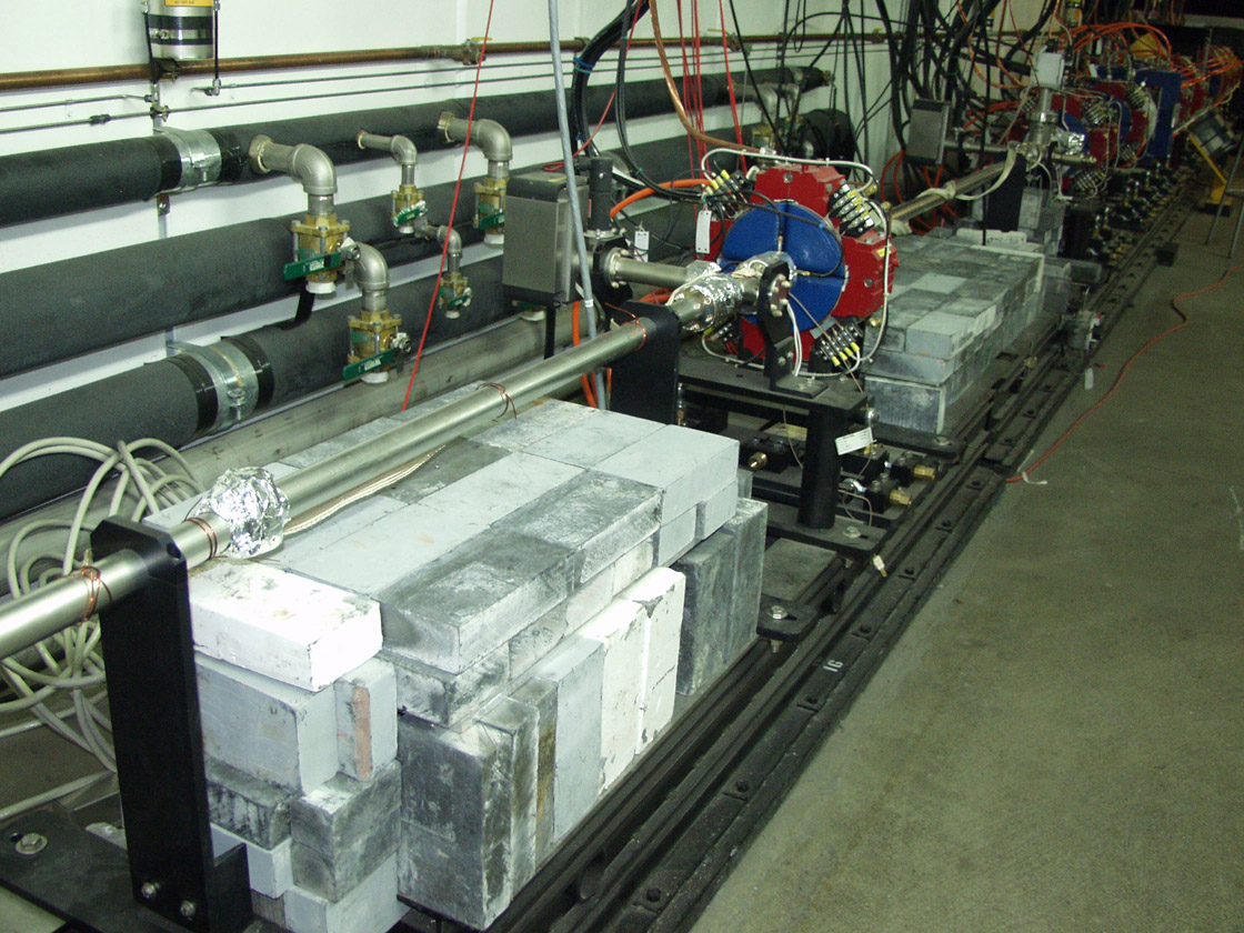
As stated in Section 3.5, the NLCTA is an entirely self contained accelerator, with its own gun, injector, chicane, accelerating structures and beam dump. A schematic diagram of the entire NLCTA can be seen in Figs. 5.1 and 5.2. Six sections of the accelerator were originally set aside for experimental X-band accelerator structures. Since only the first four of these sections of beampipe were used, FONT made use of the two remaining sections of beampipe, between quads QD1550 and QD1760: the FONT area is marked in red on Fig. 5.2. The FONT BPM, detailed extensively in Chapter 4, was installed upstream of QD1760 and Toroid 1750, as shown on Fig. 5.2; a close-up of the FONT area is shown in Fig. 5.3 (greater detail of the NLCTA stripline BPM's up and downstream of the FONT BPM location is shown on Fig. 4.32). The NLCTA beam parameters at this location are summarised in Table 3.3. As described in Section 4.3, the FONT BPM location was chosen to allow corroborative position and charge measurements to be made with stripline BPM 1760 and Toroid 1750. 4 m upstream of the FONT BPM resides QD1550 that marks the start of the FONT region.
In order to apply a deflection and correction to the beam, a method was required for creating a vertical position offset at the FONT BPM and correcting that offset. The simplest way of doing so was to steer the beam 4 m upstream of the BPM with a dipole magnet: the angular offset introduced by the dipole results in a position offset at the BPM. Having measured a position at the BPM, the FONT electronics would then transmit the corrective signal upstream to another magnet and remove the offset. These two magnets have very different requirements: the ‘offsetting’ magnet has no requirements for its response time, since one can dial in an offset well in advance of the beam. However, since it is essential to measure the repeatability of the FONT system, the long term stability of the magnet is crucial: any drift in the angular deflection applied to the beam reduces the quality of the data collected for FONT. The simplest solution was to use a standard SLC dipole magnet: details are given in Section 5.2.1. The ‘correcting’ magnet, on the other hand, must have a nanosecond level response time in order to provide a rapid correction to the beam. As such, a dipole magnet was not a realistic option. The magnet finally selected to provide the rapid position correction was a parallel plate electromagnetic kicker, similar in design to that of the real IPFB system (see Section 3.2.3); details of the magnet can be found in Section 5.2.3.
Having selected the two kinds of magnet required, the magnet arrangement had to be decided upon. From the point of view of the beam optics, the simplest option is to have both components at the same location. Normally this would not be possible, since both magnets take up a finite length of beamline: a close approximation is to have both components next to one another with nothing in between, since the position and angle difference between the two magnets is assumed to be zero over short distances. However, the magnet assembly for FONT was able to combine the two magnets into a single unit: this ensures that a particular angular deviation applied to the beam by each magnet results in exactly the same position change at the BPM. As such, there exists a direct comparison between the effect of both the ‘offsetting’ and ‘corrective’ magnets. The FONT magnet assembly is described in detail in Section 5.2.
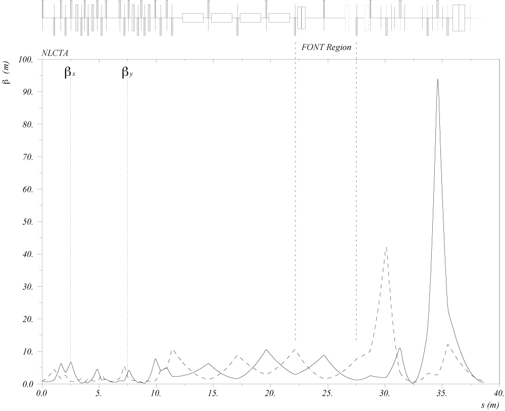
| Figure 5.4: Horizontal and vertical beta functions for the NLCTA, generated with MAD using the design lattice [106]: βx is the solid line and βy the dashed line. The FONT area begins after QD1550, at 23 m, with the FONT BPM situated upstream of QD1760 at around 27.5 m, and is marked on the figure. Note that quadrupole QD1650, situated in the centre of the FONT region at 25 m, defocuses in y. |
The NLCTA beta functions were also a motivating factor for the location of FONT. A large vertical beta function corresponds to both a large vertical beam size and position jitter [30]. To maximise the deflection seen at the FONT BPM, it is desirable to locate it at a point in the lattice with a large vertical beta function. The horizontal and vertical beta functions for the design lattice of the NLCTA are shown in Fig. 5.4. The FONT magnets, located at ~23 m, and the FONT BPM, located at ~27.5 m, are both at locations with a large vertical beta function, maximising the effectiveness of the kick.
In addition, FONT makes use of the placement of quad QD1650, situated directly between the magnet assembly and the FONT BPM. From a beam transport perspective, the beamline location of FONT is extraordinarily simple: two drift spaces are separated by a quad, for which 3 transport matrices are required to calculate the effect of the quad on the kick applied to the beam by the FONT magnets. The two drift spaces are also of identical length, since the location of the FONT magnets and the BPM is symmetrical about QD1650: the total distance between the centre of the magnet assembly and the centre of the FONT BPM was 4.18 m. From Equations 2.14 and 2.16, the effect of this beamline arrangement on the vertical beam position and angle, y and y′, is described by the following matrix equation:
| (5.1) |
where L is the distance between the magnet assembly and the BPM, Kl is the integrated field strength of the quad and Bρ is the magnetic rigidity (see Section 2.2.1). The corresponding matrix equation without the quad is simply:
| (5.2) |
By examining the beta functions in Fig. 5.4, QD1650 actually defocuses in y and the factor Kl becomes positive in Eq. (5.1). As such, assuming that the beam arrives with no vertical offset at the FONT magnet assembly (i.e. ymagnets = 0) the vertical offset seen by the FONT BPM (yBPM) as a result of a deflection applied by the FONT magnets (y′magnets) is:
| (5.3) |
The kick applied to the beam by the FONT magnets is therefore enhanced by a factor
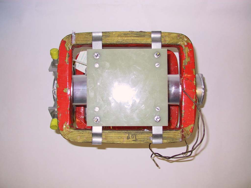
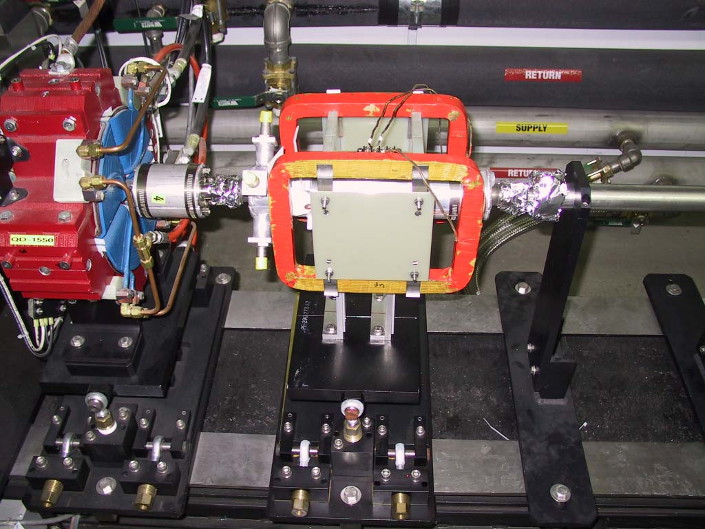
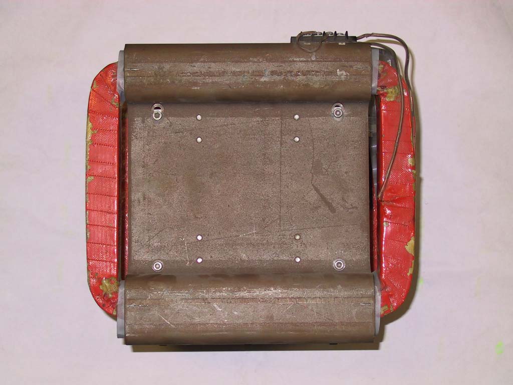
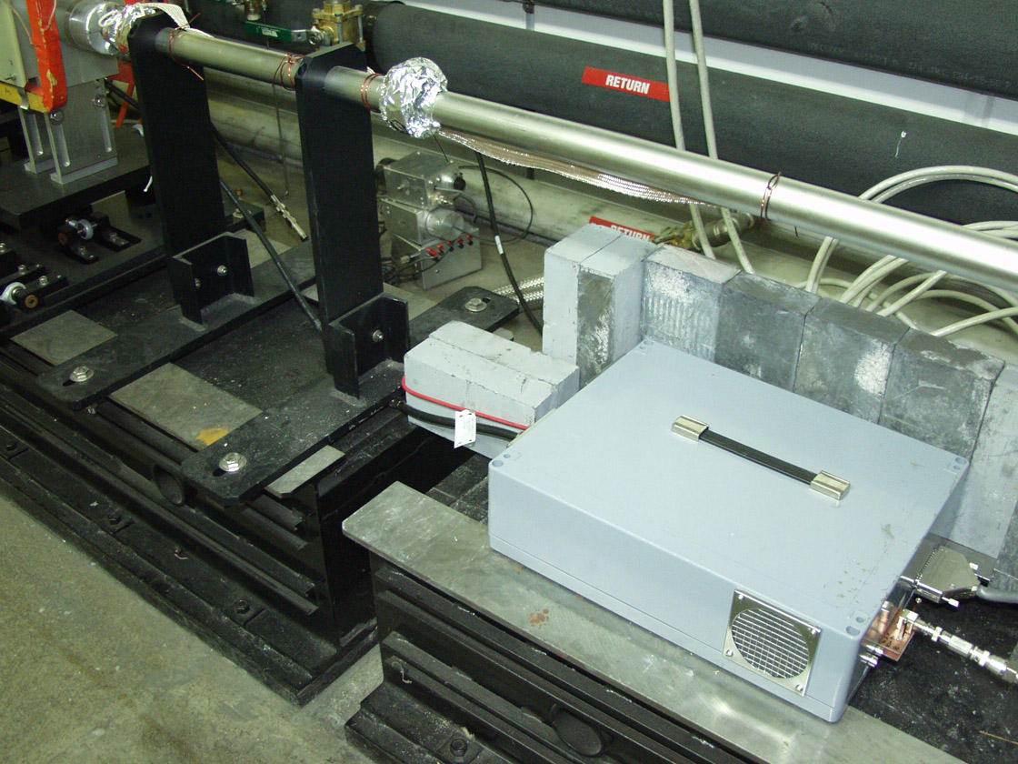
The magnet assembly is an integrated construction, consisting of the two magnet types mentioned briefly in the previous section. The full assembly can be seen in Fig. 5.5: the purpose of this integrated assembly is to combine the two FONT magnets into a single unit that steers the beam at exactly the same point. The dipole is a modified SLC Type 4 Corrector and is described in Section 5.2.1; the kicker is a standard SLC Scavenger Post Kicker Magnet, details of which are given in Section 5.2.3. The combined unit was installed in the NLCTA downstream of quad QD1550, as indicated in Fig. 5.3: a photograph of the installed magnet assembly is shown in Fig. 5.6. The construction and performance of each of the magnets is detailed in the rest of this section. Initially it was uncertain whether a separate dipole would be needed, or if it was simpler to take advantage of the dipole mode of the existing quadrupoles (namely QD1550) within the NLCTA. However, it was felt that the possibility of using a dipole that was independent of the NLCTA would give greater options for location and customisation: it would also allow the construction of the integrated magnet assembly already described.
| Figure 5.5: The FONT integrated magnet assembly. The dipole coils are red and mounted around the silver barrel of the kicker magnet. |
| Figure 5.6: The FONT integrated magnet assembly installed on the NLCTA. The assembly is mounted around a length of ceramic beampipe and is supported by two beamline support struts. The quad on the left of the picture is QD1550. |
| Figure 5.7: The SLC Type 4 Corrector magnet used in the construction of the FONT integrated magnet assembly. |
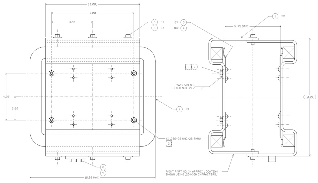
| Figure 5.8: A Schematic diagram of the SLC Type 4 Corrector. Measurements are in inches; figure adapted from [107]. |
The original construction of the SLC Type 4 Corrector is shown in Figs. 5.7 and 5.8 52. From Eq. (2.4) (see Section 2.2.1), the magnetic rigidity can be restated as:
| (5.4) |
for a momentum p in MeV. Using a small angle approximation (i.e. l = ρθ for a magnet of length l), the integrated field strength Bl, in kiloGauss-metres (kG-m), of a dipole required to steer a beam through an angle θ radians is given by:
| (5.5) |
The maximum range of beam positions measured at stripline BPM 1761 is ±4 mm: beyond this range, the beam scraping on the upstream aperture of the FONT BPM causes a large reduction in beam charge; the stripline response also becomes distinctly nonlinear (possibly as a result of this scraping). This corresponds to a maximum angular deflection at the FONT magnet assembly of 1 mrad. For the NLCTA beam energy of 62 MeV, this sets the maximum integrated field strength of the FONT dipole at 2 G-m. This places two constraints on the performance of the dipole:
The vertical beam jitter at the FONT BPM, as measured by stripline BPM 1761, is of the order of 40 microns (see Section 4.8.2 and Fig. 3.26). Since the stability of the field within a dipole is primarily dependent upon the current stability of the power supply, it is therefore necessary that the dipole power supply have a current stability of 1% within the current range required to produce the maximum dipole field. The simplest way of driving the FONT dipole was to make use of one of the existing corrector power supplies used to drive the vertical dipole of quad QD1550. In this way, the FONT dipole would be transparent to NLCTA operations, since the dipole of QD1550 is replaced with the FONT dipole just downstream (see Fig. 5.6). The power supply used to drive the correctors within the NLCTA is a 6 A Mk II 16 Channel Corrector Driver. With a maximum output of ±6 Amps, the power supply has a current stability better than 0.1% of maximum, or 6 mA, over a 24 hour period; it is also stable to much better than 0.1% over 10 minutes or so [108]. It is likely that the power supply is stable to 1% down to ~100 mA. As such, given the magnet range used for the measurements in Section 4.8.2, the full range of ±2 G-m should correspond to a power supply output of ±1 A.
|
||||||||||||||||||||||||||||||||||||||||||||||||||||
|
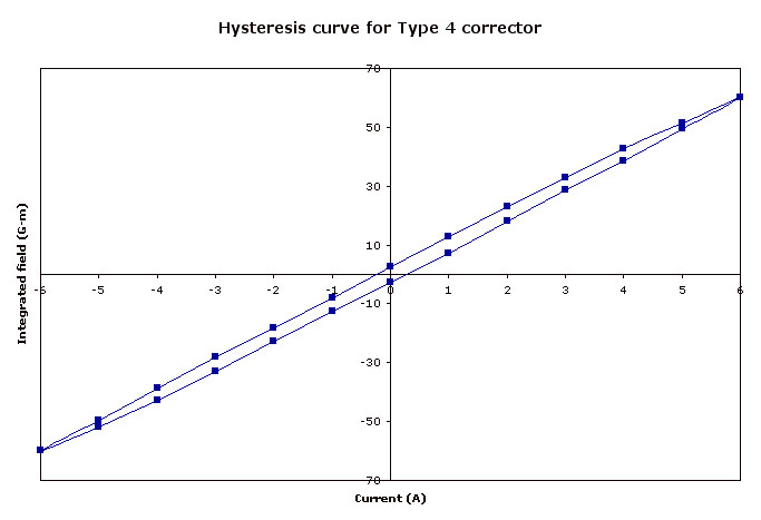
| Figure 5.9: The hysteresis curve for the Type 4 Corrector magnet, using the data shown in Table 5.1. |
Measurements were carried out on the Type 4 dipole to determine whether the magnet had the required current-field strength characteristics: these measurements are summarised in Table 5.1 [109]. The first feature to note is that the relationship between applied current and integrated field is nonlinear. This is a result of the hysteresis behaviour of the iron yoke around the dipole coils. Hysteresis arises as a result of the inherent magnetisation of all ferromagnetic solids. As such, for any ferromagnet the inherent magnetisation is not only a function of any applied magnetic field but also the previous state of magnetisation of the material, resulting in a nonlinear relationship between the applied field and inherent magnetisation [110]. The hysteresis curve resulting from the data in Table 5.1 is shown in Fig. 5.9. The purpose of the iron yoke is not only to provide a solid superstructure for the magnet coils, but also to increase the integrated field for a given current: the iron provides an easier return path for the magnetic field, meaning that less energy is required to sustain the field and leading to a higher field strength.
| Figure 5.10: Schematic diagram of the SLC Type 6 Corrector; note the yokeless design. Measurements are in inches; figure adapted from [111]. |
However, for the purposes of FONT the problems associated with the hysteresis behaviour of the magnet outweigh the advantages of the increased field strength, since a precisely, rather than approximately linear response is required. In fact, the addition of the iron yoke increases the integrated field strength above the threshold stated above: at its minimum value, a current of 1 A results in an integrated field of 7.3 G-m, significantly larger than the required field strength of 2 G-m per Amp. As a result of these measurements, the dipole's iron yoke was removed and a new support structure was designed. The construction of this dipole was based around another, smaller yokeless magnet used in the SLC, referred to as a Type 6 Corrector: a schematic diagram of this magnet is shown in Fig. 5.10. The design was modified to match the size of the coils and to expand the inner distance between the coils to 5 inches. The support structure was machined from G-10 plastic and assembled in the same way as the Type 6 Corrector: the new dipole can be seen mounted around the kicker magnet in Fig. 5.5. The new integrated field of the FONT dipole assembly was measured to be 15.50 G-m for a supply current of +6 A and 14.65 G-m at −6 A, giving an average integrated field strength of 2.51 G-m per Amp [109]. Therefore a current of 0.796 A is required to produce a field of 2 G-m, much closer to the field strength of 2 G-m/A as specified previously.
The FONT dipole was mounted tightly around the kicker magnet (details of the kicker are given in Section 5.2.3) to form an integrated unit and installed onto the NLCTA beamline, downstream of QD1550, at the same time as the FONT BPM. The installed magnet assembly with support structure is shown in Fig. 5.6. Two struts were used to support the magnet assembly, with the whole unit kept rigidly in position once it was mounted to the beampipe. The magnet was initially aligned by eye, at the time of installation, and later as part of a more rigorous NLCTA alignment procedure.
In order to measure the performance of the FONT dipole, the same procedure utilised for the FONT BPM response measurements, in Section 4.8.2, was used. Since the dipole was connected to the corrector power supply in place of the QD1550 y corrector (YCOR 1550), it could be programmed and controlled in the same fashion as any other dipole on the NLCTA. A correlation plot was set up with the SCP to record 10 beam pulses at 17 different magnet settings, using the long pulse beam. The SCP was programmed to step YCOR 1550 through 17 steps of 0.5 G-m; this range corresponds to the original 1550 y corrector, not the FONT dipole. The conversion factor required to give the field strength for the FONT dipole depends upon the gradient of each magnet: YCOR 1550 has a gradient of 6 G-m per Amp, 2.39 times larger than the gradient of 2.51 G-m per Amp for the FONT dipole53.
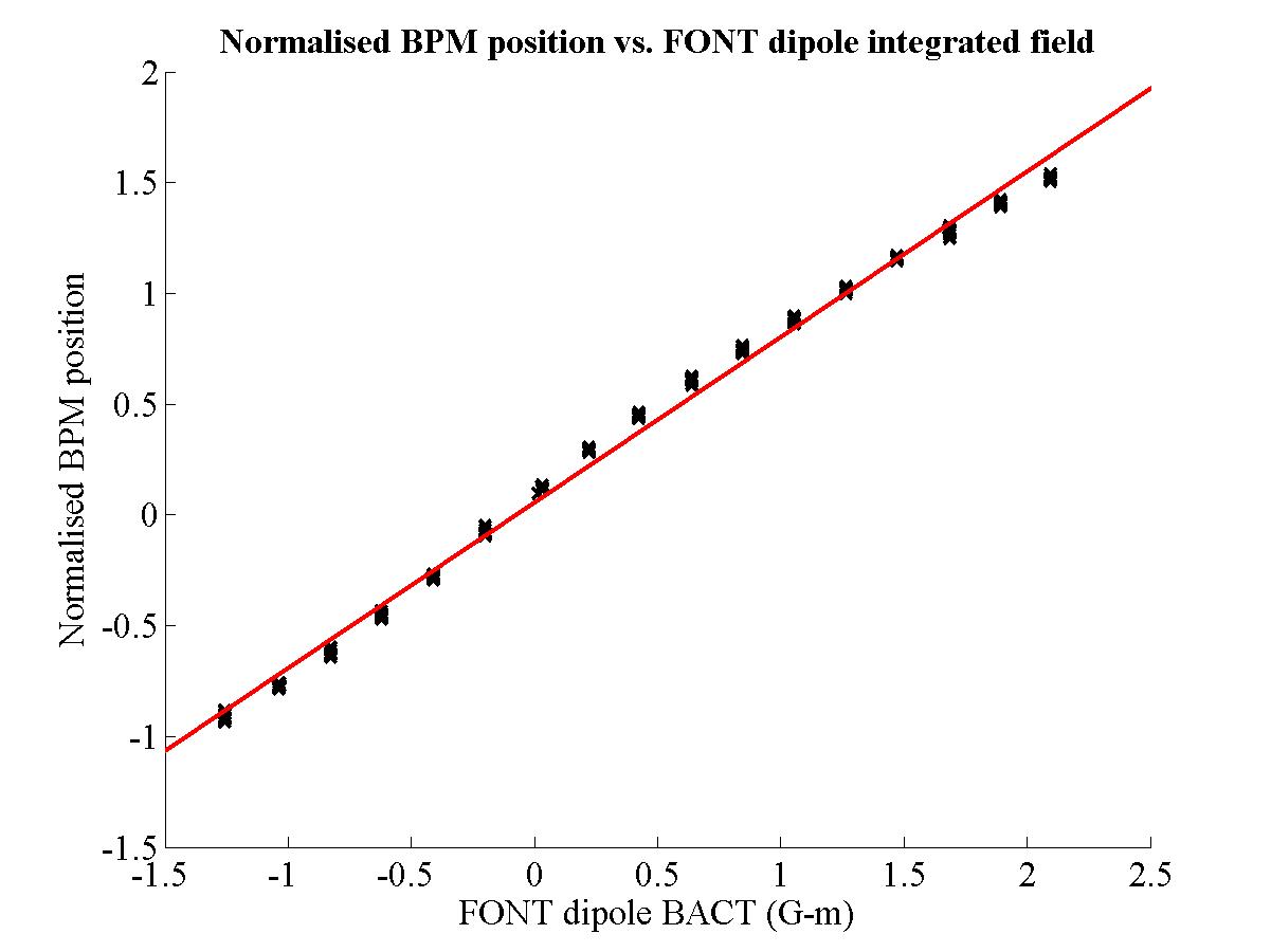
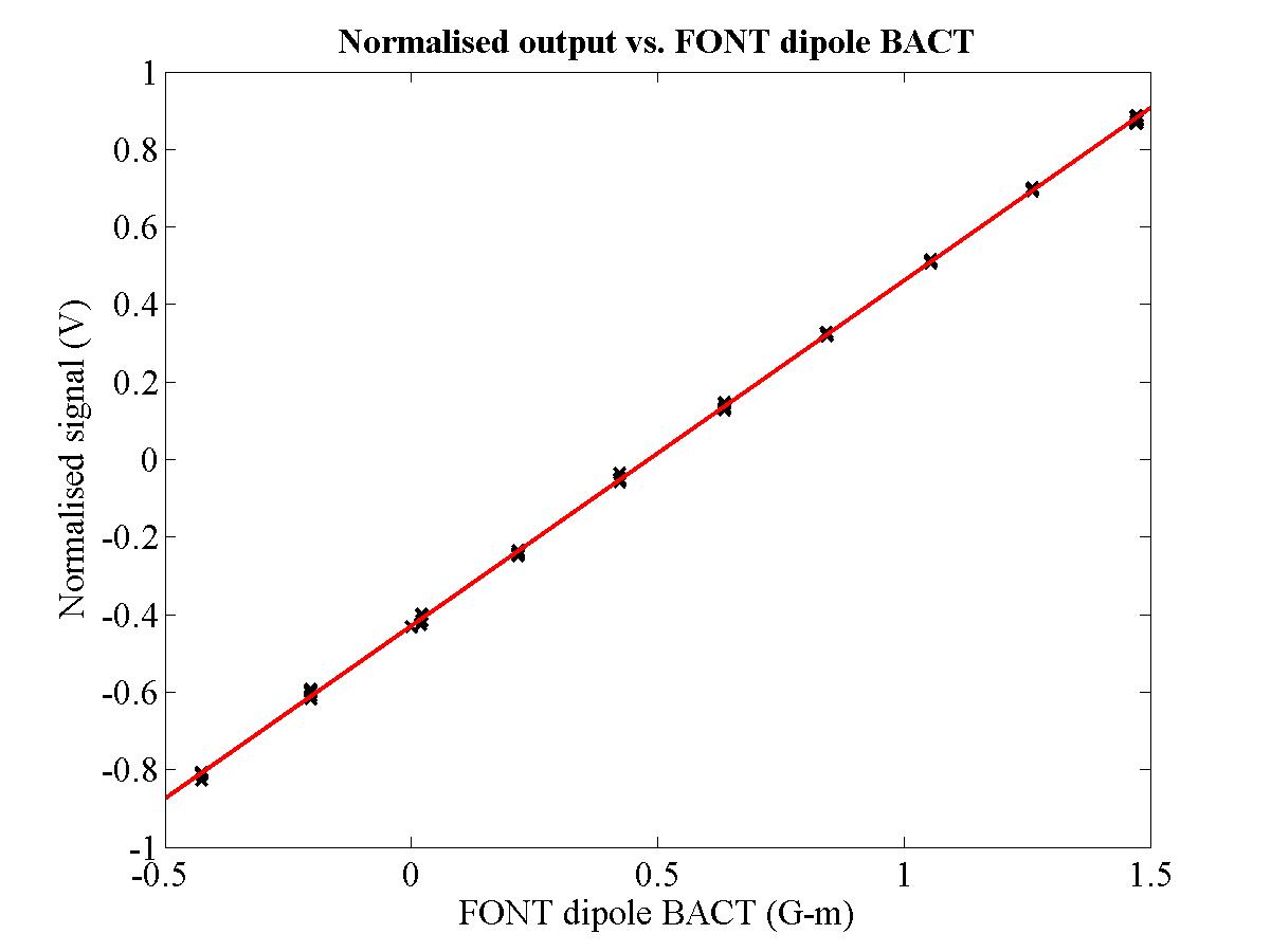
| Figure 5.11: The normalised BPM output for the long pulse beam as a function of the integrated field of the FONT dipole. The beam position of 10 beam pulses was recorded for 17 dipole settings. The red line is a line of best fit produced through a χ2 minimisation. |
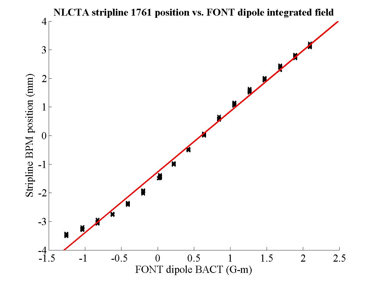
| Figure 5.12: The beam position measured by NLCTA stripline BPM 1761 as a function of the integrated field of the FONT dipole. The beam position of 10 beam pulses was recorded for 17 dipole settings. The red line is a line of best fit produced through a χ2 minimisation. |
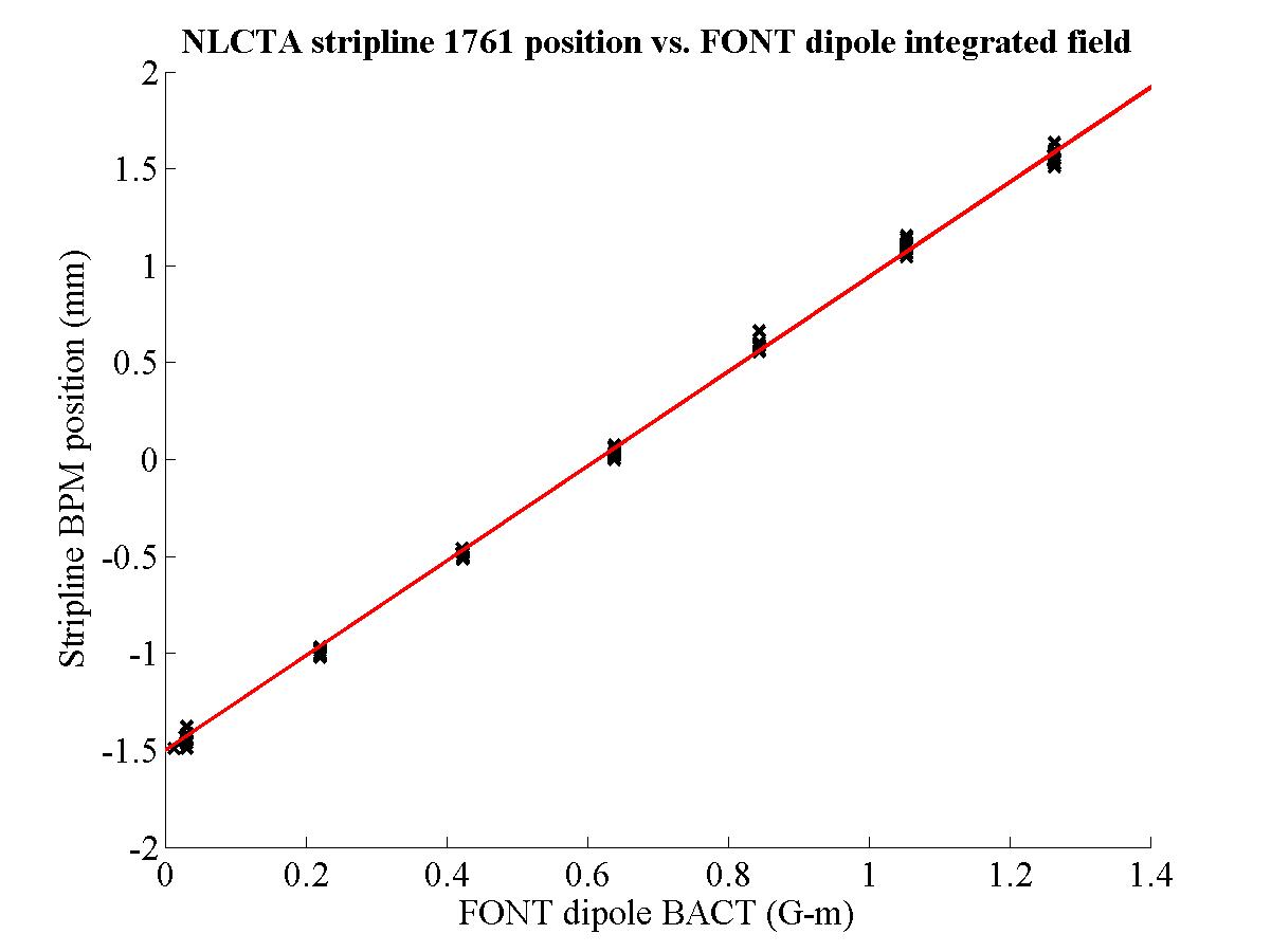
| Figure 5.13: The beam position measured by NLCTA stripline BPM 1761 as a function of the integrated field of the FONT dipole, using the central 8 dipole settings shown in Fig. 5.12. The red line is a line of best fit produced through a χ2 minimisation. |
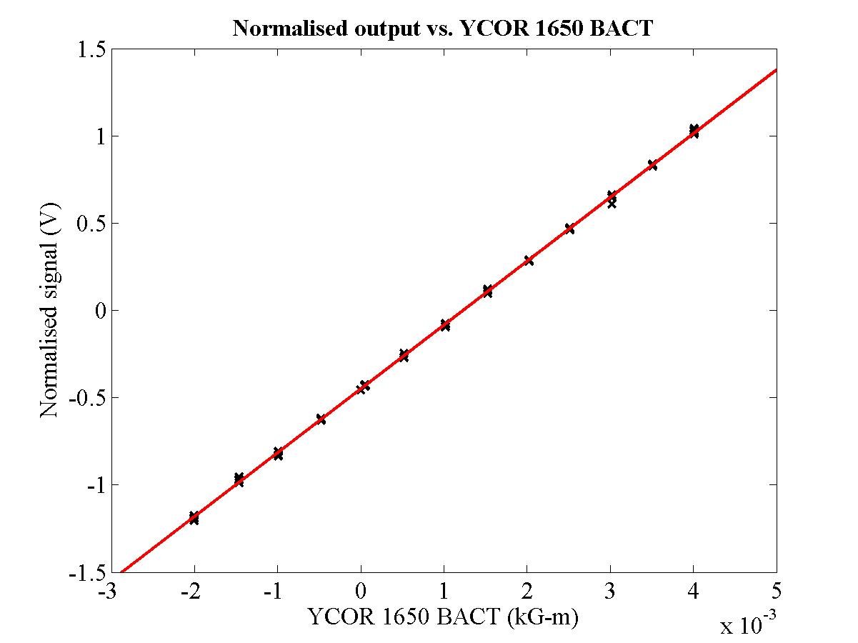
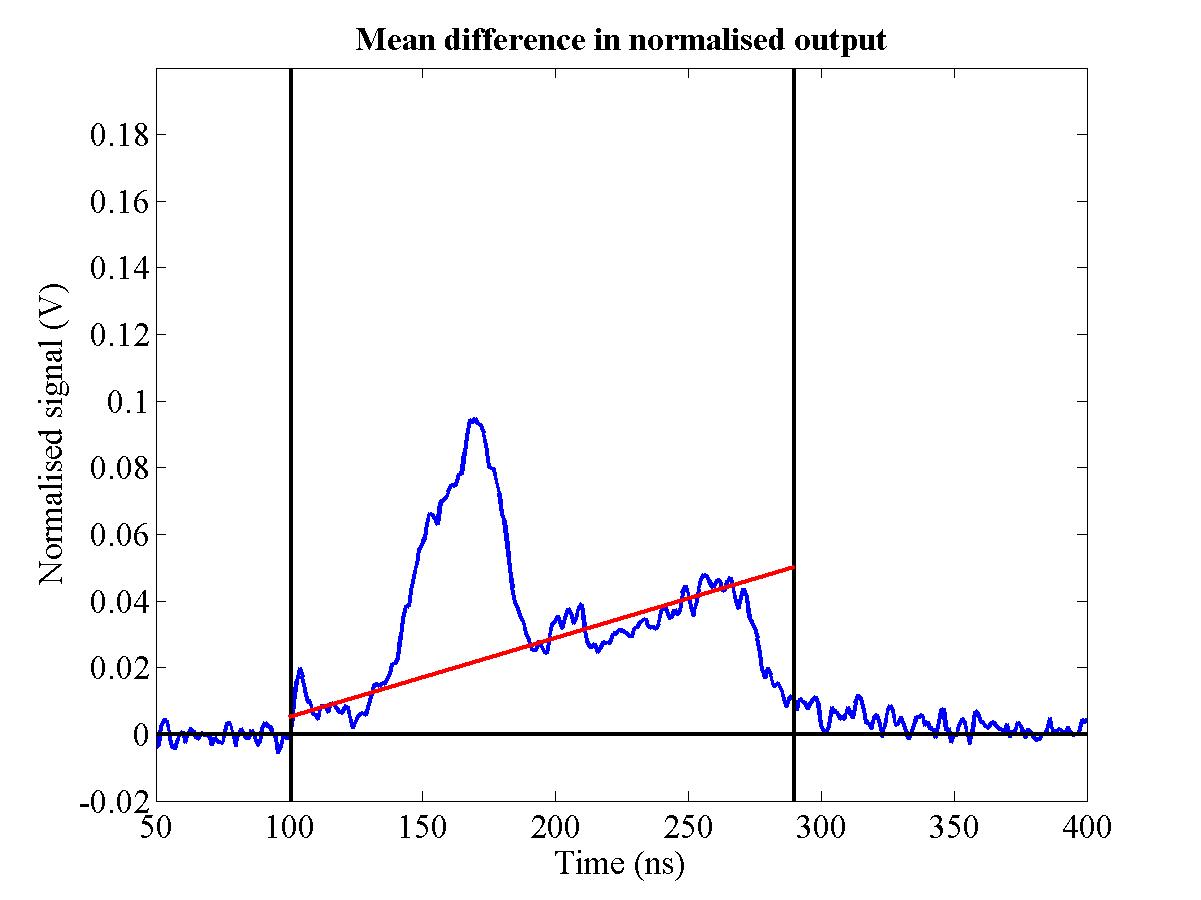
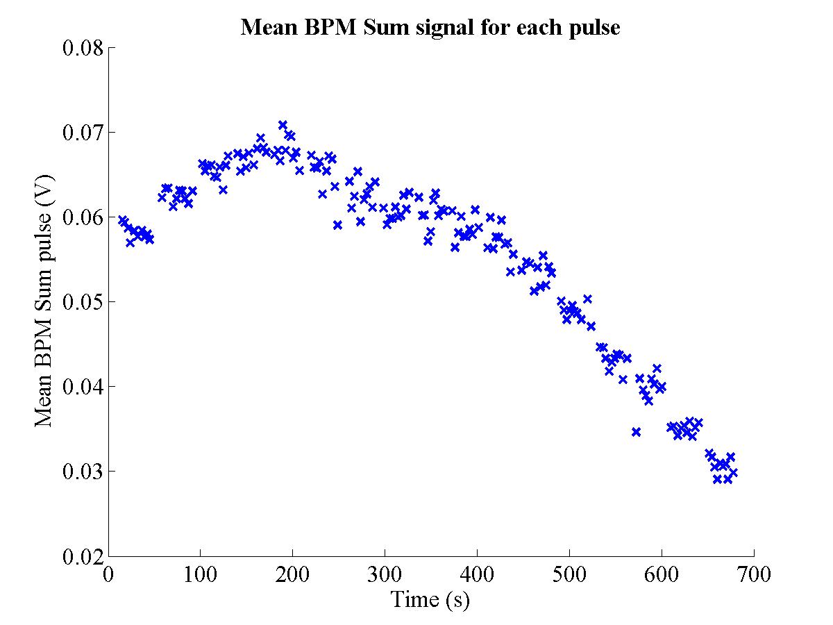
As before, the FONT BPM position was normalised by dividing the difference signal by the sum signal: the normalised pulse was then averaged between 320 ns and 440 ns (cf. Fig. 4.54) to give a single normalised position output for each pulse. A plot of the normalised FONT BPM position as a function of the calculated field strength of the FONT dipole is shown in Fig. 5.11. This plot is equivalent to Fig. 4.56 which shows the normalised position as a function of the integrated field strength of YCOR 1650. Note that, once again, the variation in dipole field produces an approximately linear response in the BPM. A more rigorous test of the performance of the dipole is shown in Fig. 5.12: here the beam position measured by stripline 1761 is plotted as a function of the calculated field strength of the FONT dipole (cf. Fig. 4.60). As before, the stripline response has a slight nonlinear ‘S’ shape to its response curve. With the knowledge that a stripline BPM has a response that is most linear with a beam close to centre, the middle 8 beam positions are plotted in Fig. 5.13. For this range of values, it is clear that there is a linear relationship between the measured beam position and the integrated field strength of the FONT dipole. As such, it is possible to conclude that the FONT dipole is operating as one would expect. It is important to note that the only effect of the intervening quad, QD1650, is to amplify the angular deflection imparted to the beam by the FONT dipole, since the data in Fig. 5.13 shows no deviation from the expected linear response.
|
|
||||
| (a) Mean sum signal | (b) Mean Toroid output | ||||
|
|||||
It is now possible to compare the field strengths and performance of the FONT dipole to YCOR 1650. The integrated field strength of YCOR 1650 required to produce a 1 mm vertical deflection, as measured by BPM 1761, is 0.93 G-m (see Fig. 4.60). The corresponding figure for the FONT dipole, using Fig. 5.13, is 0.41 G-m. This is to be expected, since there is a larger distance between the FONT dipole and BPM 1761. However, if there was no quad between the dipole and BPM, one would expect the figure for YCOR 1650 to be twice that of the FONT dipole, since it is half the distance from BPM 1761. Therefore, the beam deflection of the FONT dipole is enhanced by a factor of 1.14: this compares favourably to the predicted enhancement of 1.09 from Eq. (5.3). Clearly this enhancement will increase for a greater quad field strength: it is a matter for further investigation to determine the optimum quad strength to maximise the enhancement while still keeping the beam jitter at the FONT BPM at a reasonable level.
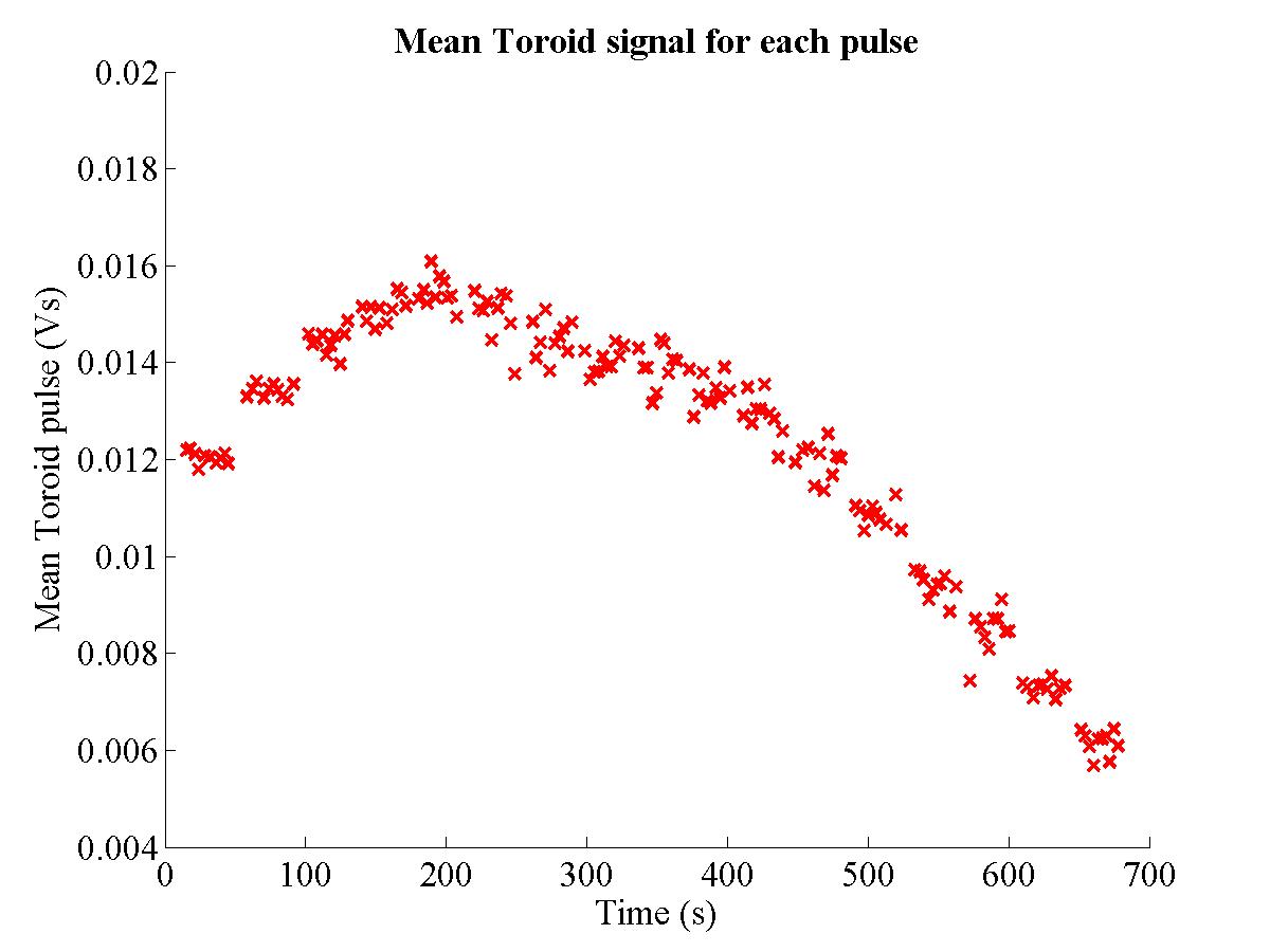
Finally it is also possible to compare the FONT BPM/stripline position response curve for YCOR 1650, shown in Fig. 4.59, to that of the FONT dipole. As before, the central 8 positions are used to determine the linearity of the normalised position measurement. Not only is this the region in which the stripline BPM is most likely to be linear, it is also the range in which the beam charge (and hence the sum signal) is large enough to accurately calculate the normalised position. The charge measurement for the FONT dipole dataset is shown in Fig. 5.14 (cf. Fig. 4.57): note that, after ~400 s, the charge deteriorates significantly54. The normalised and measured stripline positions for each pulse are shown on Fig. 5.15 for the FONT dipole measurements. For YCOR 1650 the relationship 0.299 ± 0.012 BPM units = 1 mm was measured. The relationship for the FONT dipole dataset is 0.314 ± 0.011 BPM units = 1 mm (see footnote 51). The close match between these two measurements is another indication that the FONT BPM correctly measures beam position.
| Figure 5.16: The SLC Scavenger Post Kicker magnet used in the construction of the FONT integrated magnet assembly. The input connectors are covered by yellow protective caps, on the right hand end of the kicker barrel. |
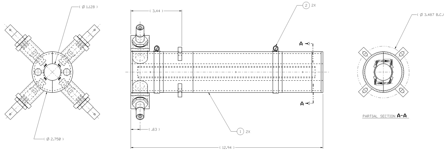
| Figure 5.17: A Schematic diagram of the SLC Scavenger Post Kicker. The kicker plates are approximately 30 cm in length; measurements are in inches. Figure adapted from [112]. |
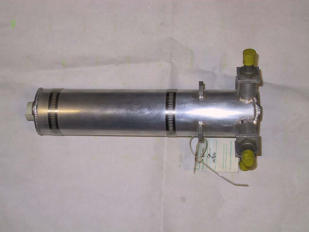
The kicker magnet used as the ‘corrective’ magnet for FONT was an SLC Scavenger Post stripline kicker. This type of magnet is used within the SLC Damping Rings to allow fast extraction of the beam from the ring. It is a parallel plate design, similar to that detailed for the real IPFB system in Section 3.2.3, and was acquired along with the Type 4 dipole 55. The kicker is shown in Fig. 5.16, with the corresponding schematic diagram shown in Fig. 5.17. The barrel of the kicker is split into two halves along its length, each of which contains a single stripline: the two halves are connected electrically by a pair of pins — one on each half — that protrude from the body of the barrel and connect to the other half. When installed on the beamline, the kicker barrel is mounted around a length of ceramic beampipe that allows the field from the plates to penetrate into the beampipe (see Fig. 5.6). The kicker plates are ~30 cm long, with an inner radius of 14.3 mm.
Unlike the electrostatic IPFB kicker design, the scavenger post kicker is electromagnetic. An external voltage is connected to the input connectors of the magnet: these are the yellow-capped prongs that protrude from the main kicker barrel (see Fig. 5.16). The voltage is applied through one pair of connectors attached to one half of the kicker barrel and coupled out through the connectors attached to the other half of the barrel. The current flows into the kicker through the input connectors, along one strip, through the connecting pins, into the other strip and out of the kicker through the output connectors56. As such, the kick applied to the beam is a result of the magnetic field generated by the current flowing in the striplines. As a result, the kicker was predicted to have a fill time of around 2 ns, similar to that specified for the IPFB kicker (see Section 3.2.3) [113]. The fill time arises from the time taken for the voltage pulse to travel the full 60 cm from input to output connector. The kick applied to the beam by the magnetic field generated by the kicker can be calculated in the following way. The magnetic field dB at a distance r due to a current I in an element ds of an infinitely long straight wire is given by:
| (5.6) |
where μ0 = 4π×10−7 is the permeability of free space [41]. Therefore, if the current flows in a stripline directly above the beam trajectory, the B-field in Tesla experienced by the beam is entirely transverse, in the horizontal direction, and reduces to:
| (5.7) |
since the beam travels parallel to the kicker plate and hence the current flow. For a kicker with two equal plates of length L, with an impedance R and gap width d = 2r and assuming that the beam is exactly centred between the two plates, the integrated field is given by:
| (5.8) |
for an integrated field in kG-m57. For the FONT kicker, with impedance R = 50 Ω, gap width d = 28.7 mm and plate length L = 30 cm there is the following relation between integrated field and applied voltage:
| (5.9) |
As such, there should be a direct comparison possible between the FONT dipole and kicker. In addition, it is possible to calculate the beam deflection as a function of applied voltage by making using of Eq. (5.5):
| (5.10) |
For the NLCTA beam, with a beam energy of 62 MeV, the angular deflection imparted to the beam should have the following voltage dependence:
| (5.11) |
Since the original integration was carried out for an infinite current carrying wire, these approximations represent an upper limit on the kick imparted by the kicker. The true figure is likely to be reduced by a factor of 0.8-0.9 [43]; however, Eqs. 5.10 and 5.11 should be comparable with the measured beam deflection given in the next section.
Although the kicker was eventually intended for use with the FONT fast feedback system (see Section 5.1), a standalone power supply was used to test the kicker. The voltage supply used was a Q-switch/Cavity Dumper58: this sort of power supply is normally used as the high speed voltage source for a Pockels cell59. The power supply was designed to provide a kV voltage pulse up to 300 ns in length and a fall time of < 10 ns, with a very smooth falling edge. The power supply had a maximum output of ~1.4 kV but was primarily run between 0 and 1000 V for the purposes of the FONT tests. A DC input of 0-10 V is required to select the output voltage, input via a connector on the rear of the unit. A NIM pulse is used to trigger the output voltage pulse, the length of which sets the duration of the Q-switch output. The power supply was located outside the tunnel, with the output connected to a length of 3/8-in. heliax cable that was run into the tunnel and connected to one of the input connectors of the kicker magnet. The return cable (also 3/8-in. heliax), connected to one of the output connectors of the kicker, was terminated in a 2.5 kV Barth Electronics 50 Ω terminator via a 100:1 pickoff: this pickoff allowed the voltage output of the power supply to be measured and recorded.
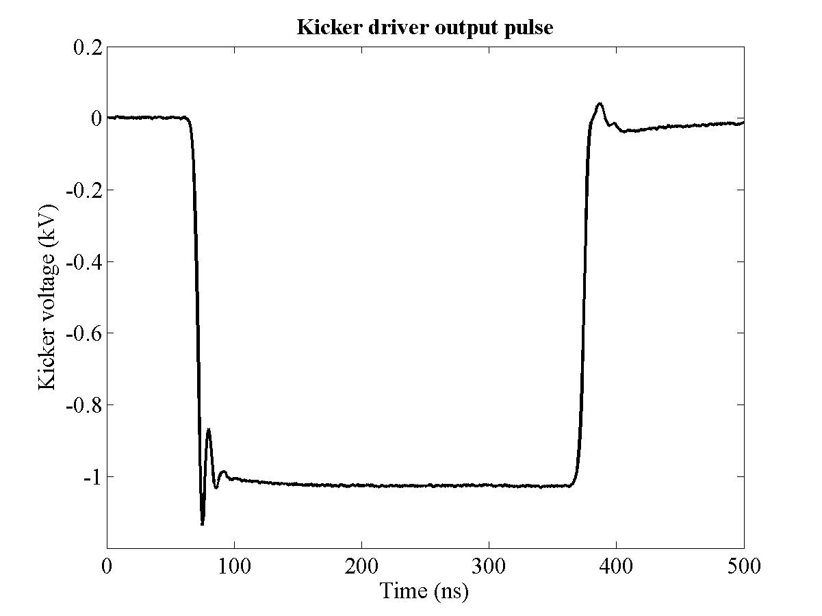
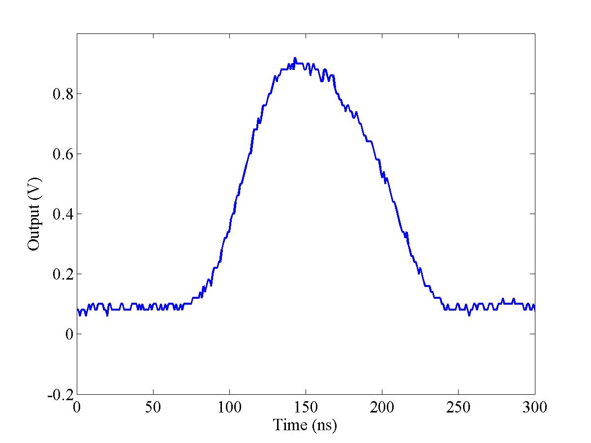
| Figure 5.18: The voltage output of the Q-switch power supply used to drive the kicker magnet. Note that the pulse has an approximately flat plateau of ~200 ns. |
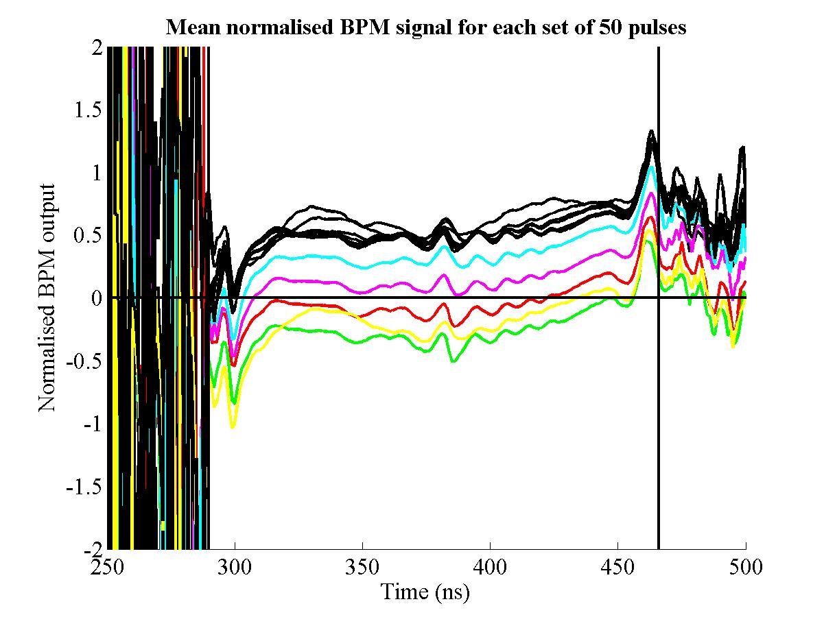
The output of the Q-switch power supply is shown in Fig. 5.18. The leading edge of the Q-switch pulse shows a large amount of ringing. The trailing edge, however, shows a smoother and more rapid voltage drop, with less ringing than is seen on the leading edge. As such, the trailing edge of the kicker pulse was used for all the kicker magnet tests: a kicker pulse with very few features was desirable in order that any ripple on the kicker pulse would not cause significant additional beam motion. A number of different beam pulses were recorded with different kicker voltages and timings. Initially the timing was set up so that the kicker pulse was applied to the whole 170 ns beam pulse. 4 different voltages, from −250 V to −1000 V in steps of 250 V, were used with 50 beam pulses recorded for each voltage; two sets of data were recorded for the −1000 V kick. For each of these kicker voltages, a corresponding set of 50 pulses was recorded with the kicker off to give a baseline measurement for each kicker voltage. The kicker timing was then changed so that the kicker pulse would switch off in the middle of the beam pulse to observe the smoothness of the kicker pulse transition.
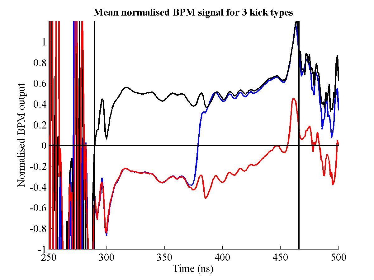
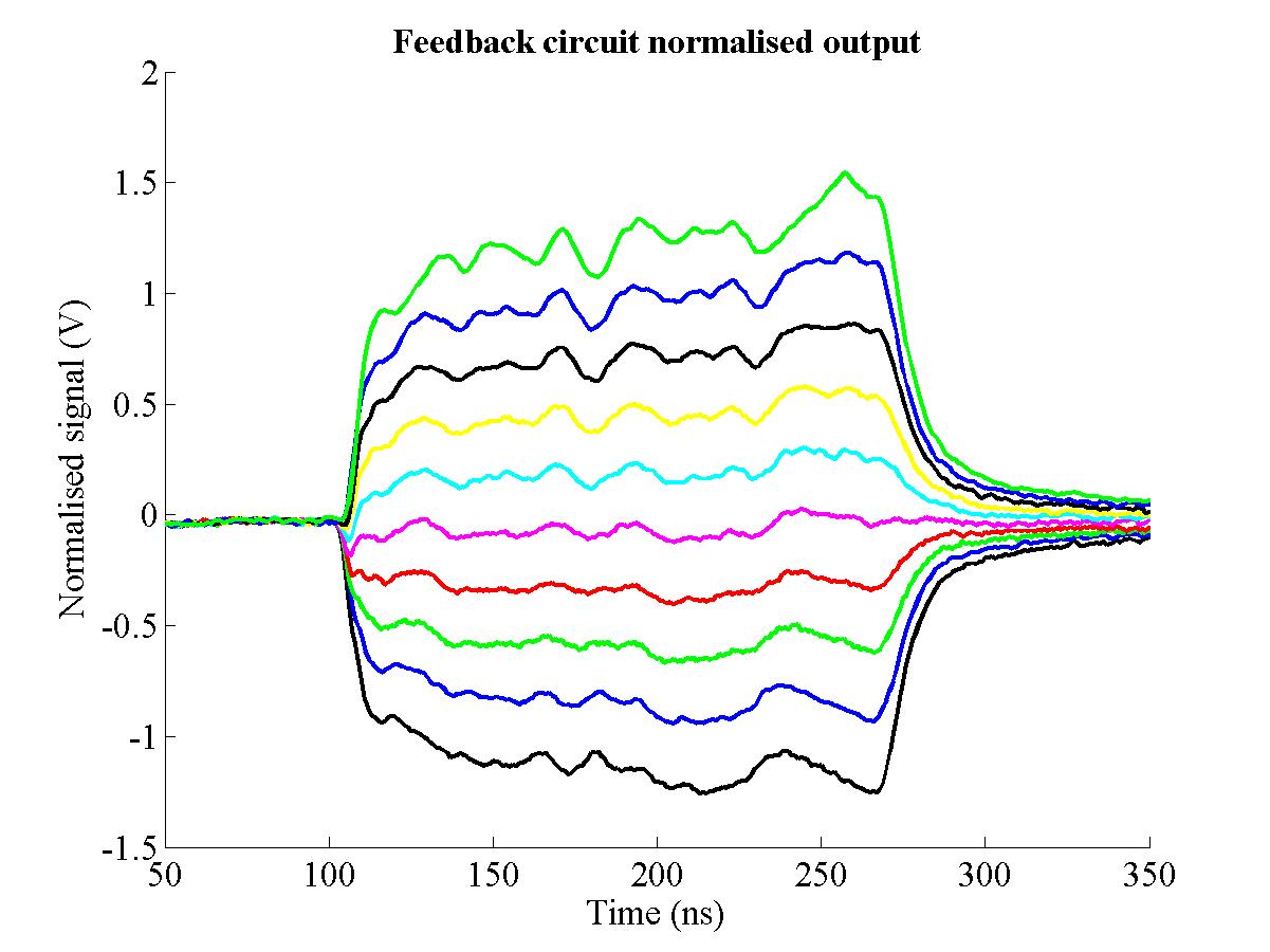
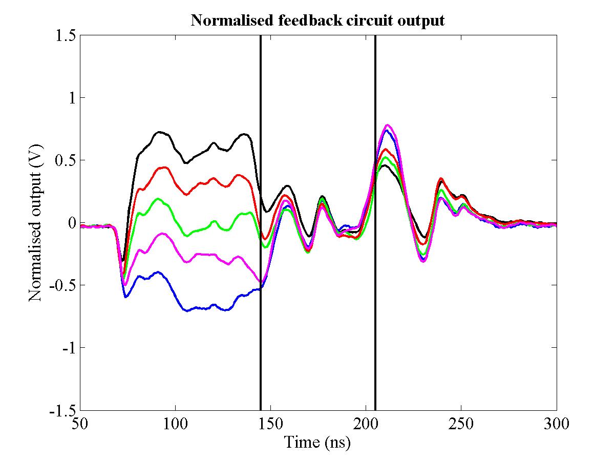
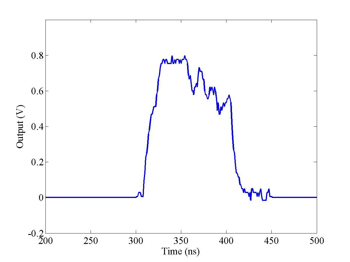
| Figure 5.19: The normalised FONT BPM position for three different kicker voltages. A full −1000 V kick is shown in red; the corresponding baseline is shown in black. The blue trace shows the effect of a −1000 V kick switching off in the middle of the pulse at ~375 ns. Each trace is the average of 50 pulses. |
| Figure 5.20: The normalised FONT BPM position for a number of different kicker voltages. The coloured traces show the effect of the kicker on the beam; the black traces are the baseline measurements. Each trace is the average of 50 pulses; the normalised position is calculated in the same way as before (see Section 5.2.2). |
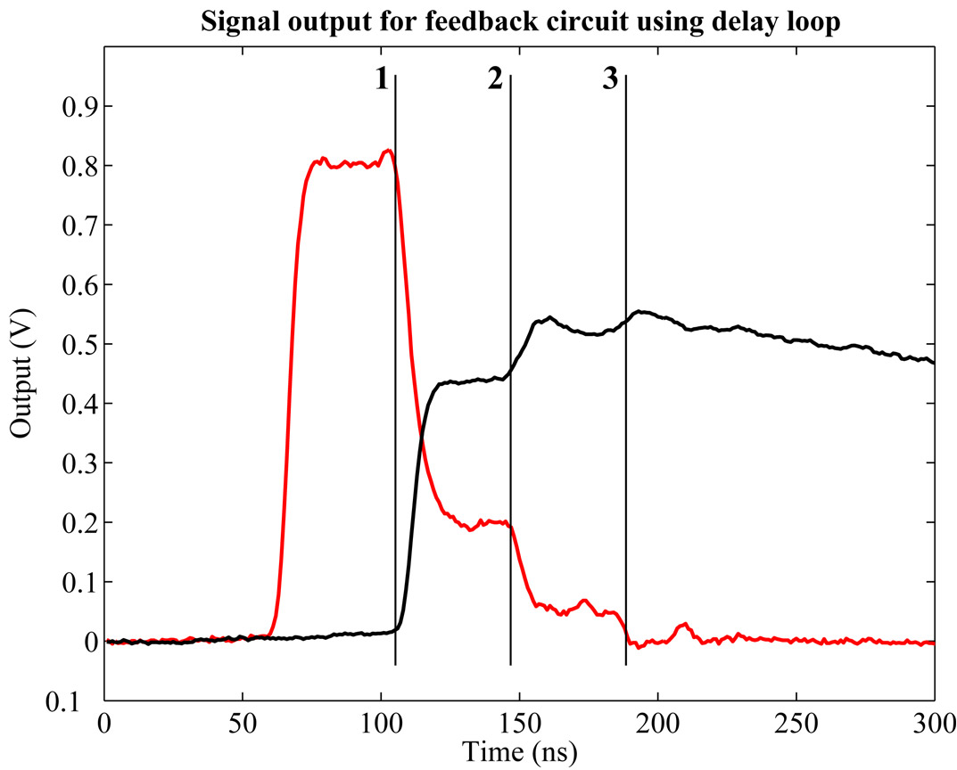
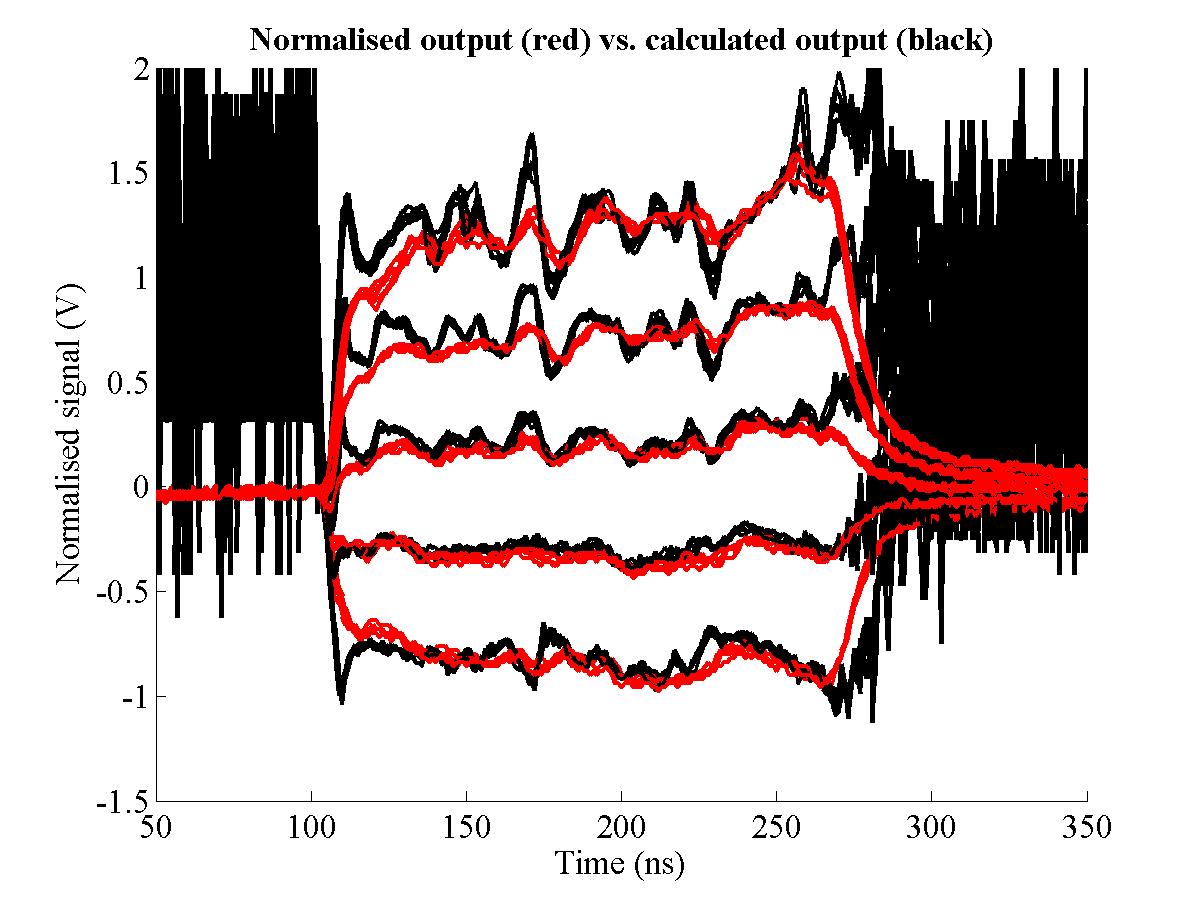
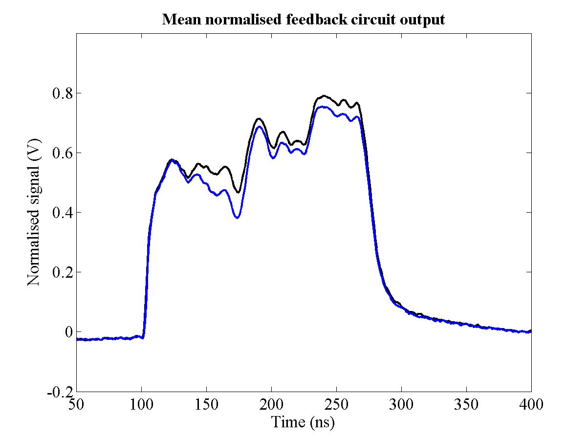
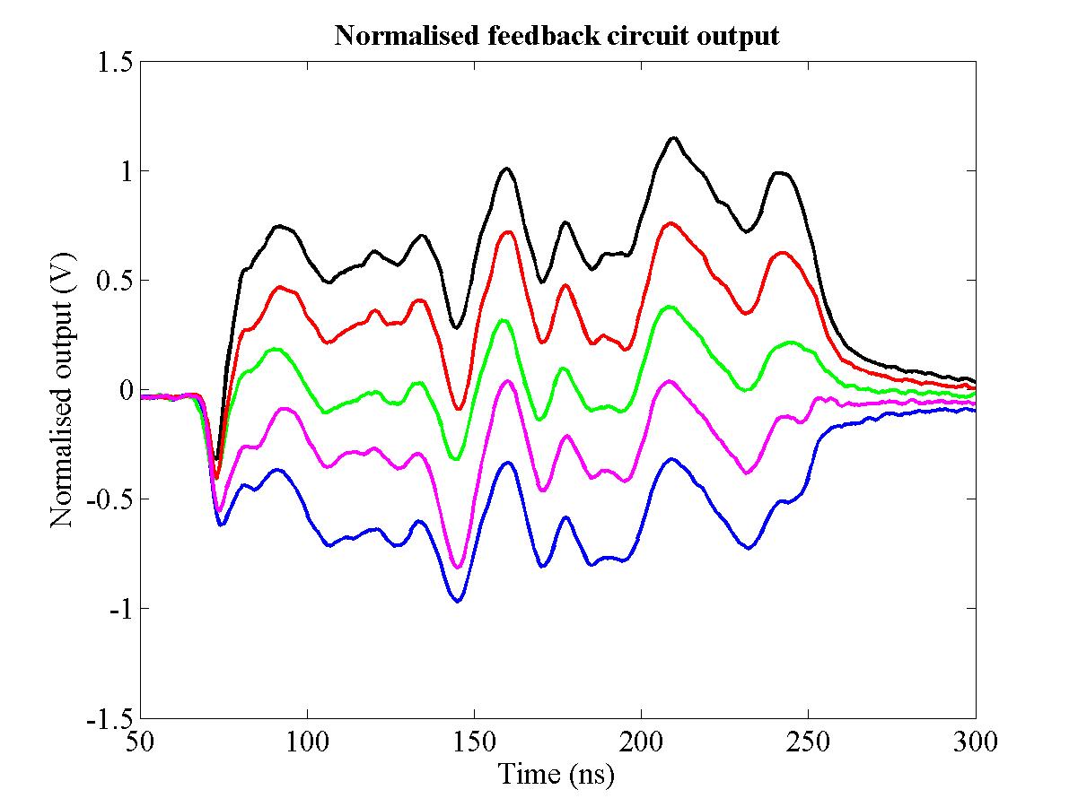
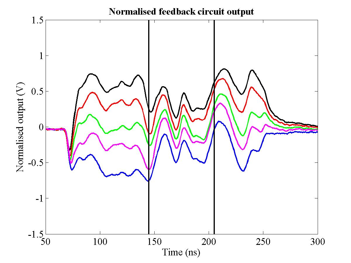
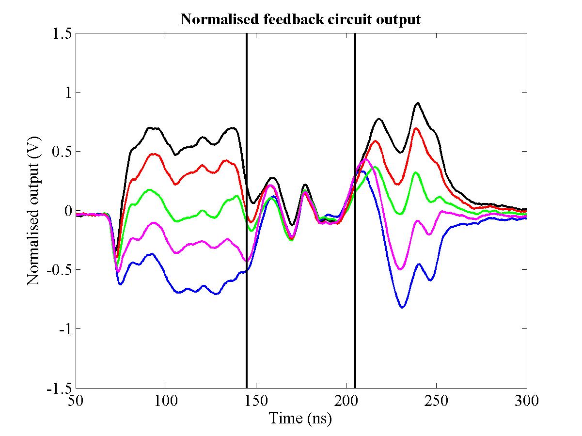
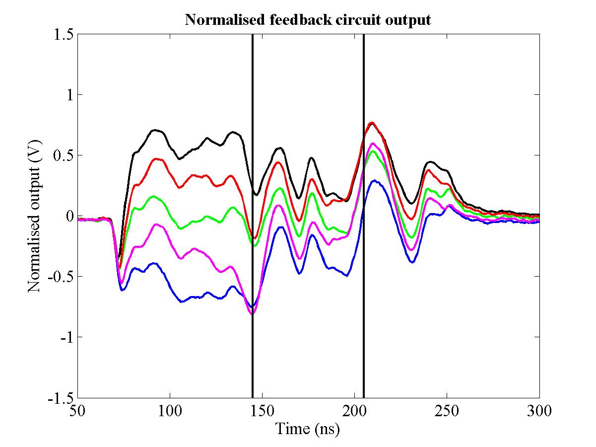
The normalised FONT BPM position for three of the kicker voltages can be seen in Fig. 5.19. Here the effect of the kicker on beam position can be seen quite clearly. The black trace shows one of the datasets with no kick: the corresponding beam position for a −1000 V kick is shown in red. Although the beam position is far from smooth, the features that appear on the first trace are clearly replicated on the second, indicating that the kicker is operating correctly. As a further demonstration of the kicker operation, the blue trace shows the effect of the kicker being switched off in the middle of the beam pulse. Note that, up to 375 ns, the pulse very closely matches the kicked beam position. Once the kicker is switched off, the beam is no longer steered downwards and the beam moves rapidly to closely match the beam pulse with no applied kick. The full dataset is shown in Fig. 5.20: as with the dipole position measurements, there is a clear ‘stepping’ of the normalised beam position that corresponds to the changing kicker voltage.
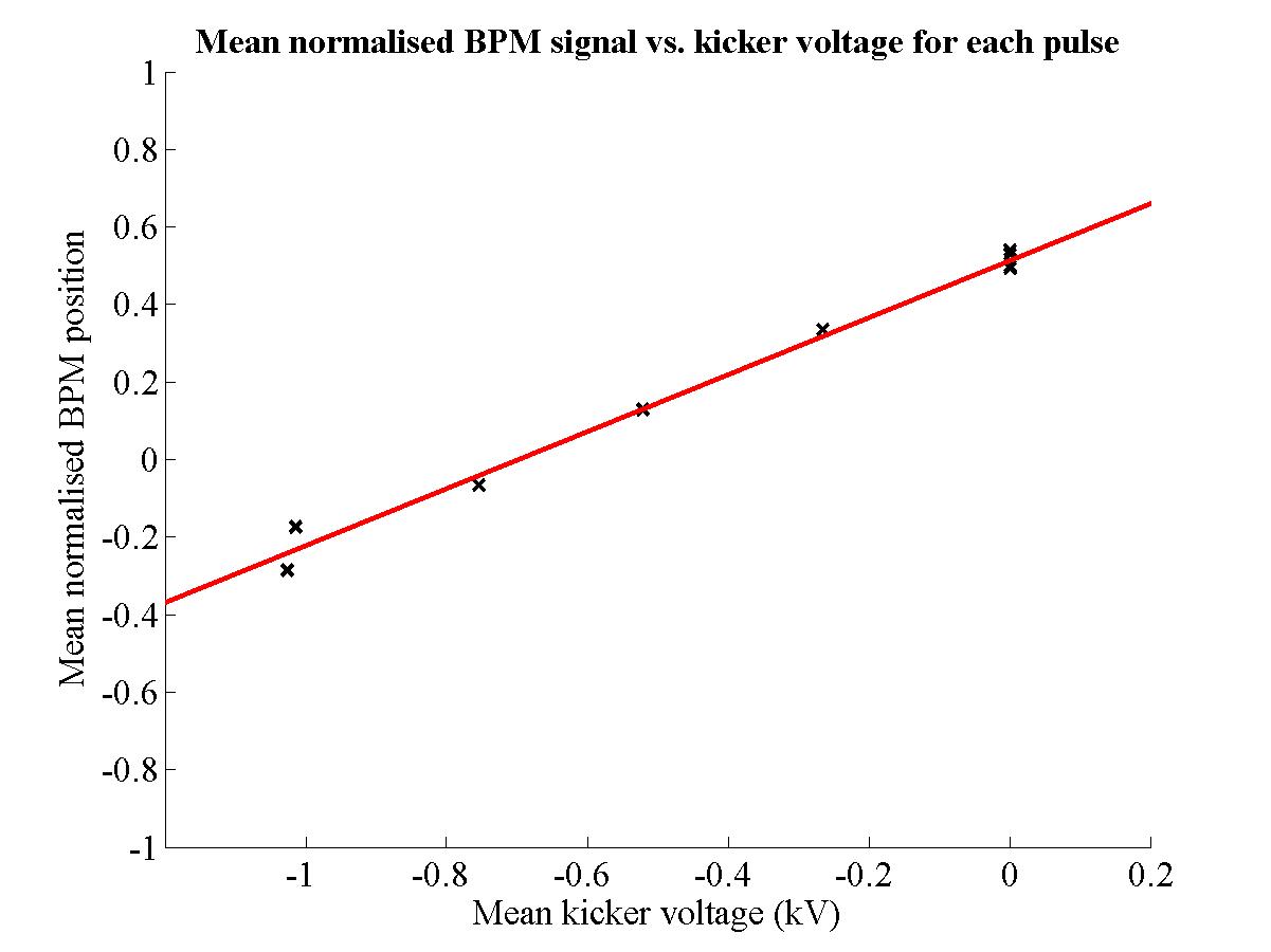
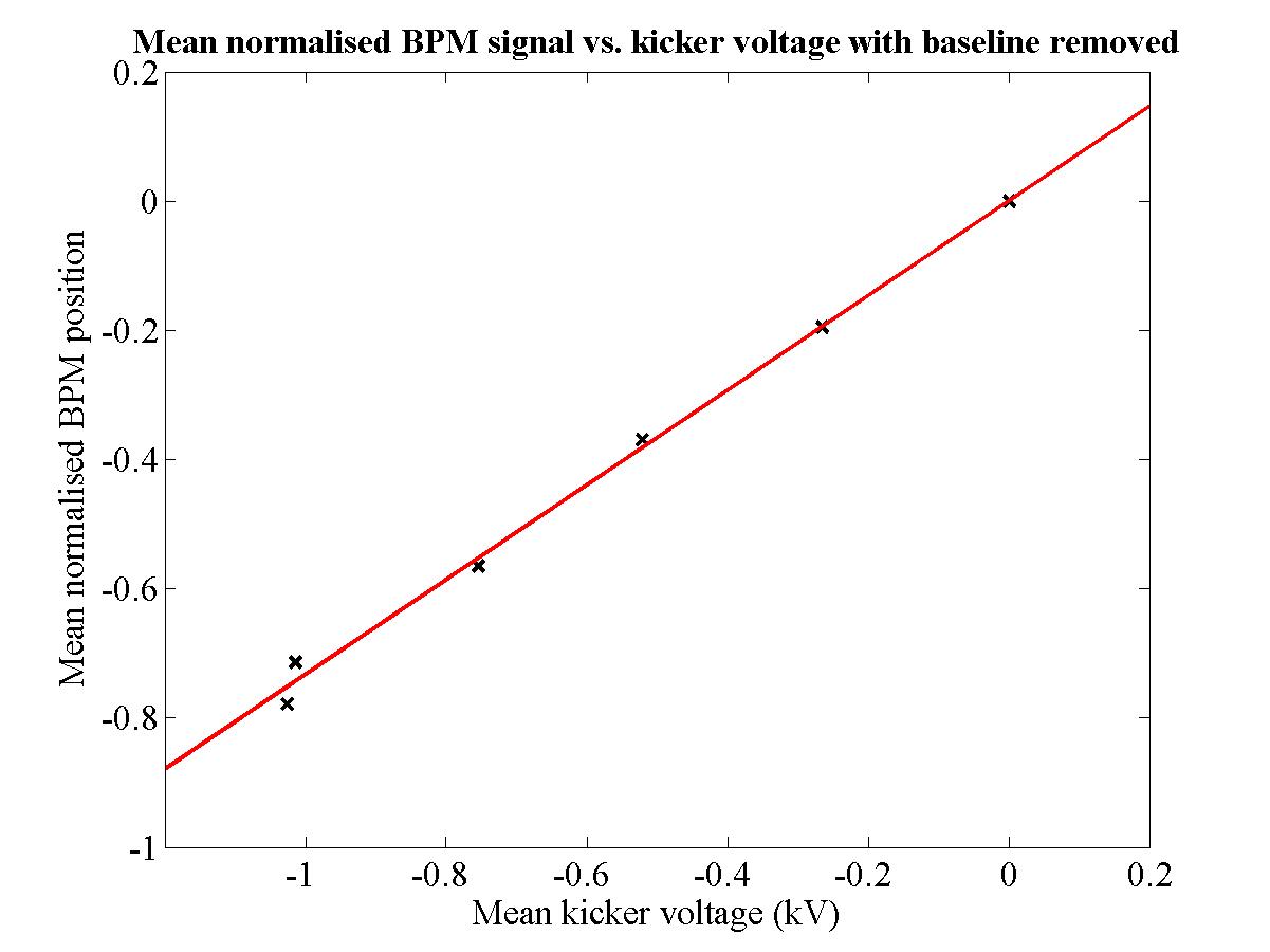
The effect of the kicker on beam position can be measured by comparing the applied kicker voltage to the mean normalised beam position response that is produced. As before, the mean normalised beam position for each pulse is produced by averaging the normalised position between 320 ns and 440 ns (cf. Section 4.8.2). This mean normalised position, for each dataset of 50 pulses, is shown as a function of the applied kicker voltage in Fig. 5.21. Note that there is a clearly linear relationship between the applied kick and the measured change in beam position, as one would expect from Eq. (5.11). This figure, however, is not necessarily a true indication of the effect of the kicker, since it does not take into account the temporal drift of the beam. As such, the mean normalised position was recalculated by subtracting the baseline measurement: for each set of beam pulses with the kicker on, the corresponding dataset without the kicker is subtracted to remove any beam effects and show only the effect of the kicker. The effect of this baseline subtraction is shown in Fig. 5.22. Note that there is an improved correlation between the data and the fitted line. From this figure, a normalised beam position variation of 0.733 BPM units is measured for a kicker voltage of 1000 V (the corresponding value for Fig. 5.21 is 0.735 BPM units per 1000 V).
| Figure 5.21: The normalised FONT BPM position as a function of kicker voltage. The red line is a line of best fit produced through a χ2 minimisation; each point is the average of 50 pulses. |
| Figure 5.22: The normalised FONT BPM position as a function of kicker voltage, using the baseline subtraction. For each set of beam pulses with the kicker on, the corresponding dataset without the kicker is subtracted to remove any beam effects and show only the effect of the kicker. The red line is a line of best fit produced through a χ2 minimisation. |
It is now possible to measure the true position variation produced by the kicker. The gradient of Fig. 5.15 gives the normalised position dependence of 0.314 BPM units = 1 mm. Therefore, a 1000 V kick corresponds to a position change of 2.33 mm. It is also possible to draw a comparison between the effect of the kicker and that of the FONT dipole measured in Section 5.2.2. Using the data from Fig. 5.11, a variation in normalised position of 0.733 BPM units corresponds to an integrated field of 9.81×10⁻⁴ kG-m. Therefore the kicker produces an integrated field of 9.81×10⁻⁷ kG-m/V. Comparison with the result derived in Eq. (5.9) of 1.68×10⁻⁶ kG-m/V shows a reasonable match between the theoretical prediction and measured value. The discrepancy between these two figures is probably a result of the finite length of the kicker striplines, since the B-field was calculated for an infinite current carrying wire. There is also likely to be a further reduction due to both the curved geometry of the striplines (see Fig. 5.17) and the energy loss through eddy currents within the metal body of the kicker barrel [43].
In order to translate the IPFB system onto the NLCTA for FONT, a number of modifications had to be made to the original IPFB design. For the IPFB system, the beam position is extracted through the same Δ/Σ method as is used to produce the normalised X-band BPM response. The suggested method is to use a programmable attenuator to modify Δ by 1/Σ and retrieve the charge information from the damping rings before the beam arrives at the IP (see Section 3.2.2 and [58]). However, for the measurements made with the BPM in Section 5.2 and Chapter 4, this charge division was carried out offline, once the data acquisition had been completed. For a real time charge division to take place, the charge information must somehow be provided before the beam reaches the BPM, since it is not possible to use the IPFB method. In addition, the requirements for the FONT kicker amplifier are considerably more demanding than for the real IPFB system. As described in Section 3.2.3, a 10σy beam deflection at the IP requires a power of just over 10 W. In order to steer the beam a millimetre at the NLCTA, a 1.6 kW amplifier is required, with a similar rise time (~5 ns) to the real IPFB kicker amplifier.
A specially designed kicker amplifier had to be utilised for FONT to provide the necessary power and rise time: this amplifier design is described in Section 5.3.5. A two-stage solution was proposed, by Josef Frisch and Gavin Nesom, to the charge normalisation problem. The first stage was to make use of the charge signal from a previous pulse. As can be seen from the long pulse position response in Section 4.8 (particularly Fig. 4.55), while there may be a good deal of variation in charge and position over the length of the pulse, the pulse-to-pulse stability is usually very good. Therefore using the sum signal from a previous measurement is a satisfactory alternative to using the real sum signal for a given pulse. The second problem is to deliver this inverted charge signal to the normalisation circuit (see below). While a multiplication is possible to achieve electronically at the required speed (~1 ns), implementing a division is not nearly so straightforward. Since a delay had been introduced by choosing to use the sum signal from a previous pulse, this opened up the option of inverting the sum signal in software, before passing it back to the normalisation circuit to be multiplied with the difference signal and produce the required normalised position. The sum signal could therefore be recorded by a PC running Matlab and the inverted charge signal calculated. By using the GPIB capability of Matlab, an Arbitrary Waveform Generator (AWG) could be programmed with this inverted waveform and then used to output the inverted sum signal to the normalisation circuit: this was the scheme that was used for FONT.
The complete FONT system consists of the following components:
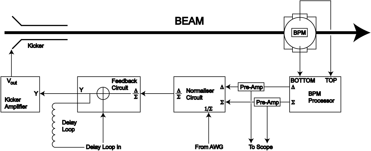
| Figure 5.23: A block diagram of the FONT feedback system; see main text for details (refer to Fig. 4.28 for details of the BPM processor). |
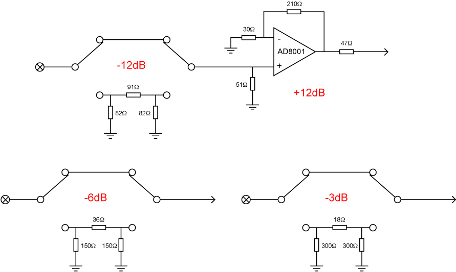
The BPM processor operates as before, taking the X-band BPM raw top and bottom pickoff signals as its inputs and outputs the sum and difference of the two input signals. These sum and difference signals are then amplified by a pair of signal pre-amplifiers that boost the signals up to the required level for the normalisation circuit. The signal is then split at the output of the pre-amps, half the signal going to the normaliser and half being output to an oscilloscope outside the tunnel as part of the DAQ system. The normaliser circuit multiplies the difference signal by the inverted sum signal, provided by the AWG, and makes an additional first-order correction using the current sum signal (see Section 5.3.1). The normalised output (Δ/Σ) is passed on to the feedback circuit, which adds the current normalised position to that measured during the previous latency period. This signal is then amplified by the kicker amplifier, which drives the kicker magnet and steers the beam to correct the position at the BPM. The whole process then repeats for as long as the bunch train lasts and the BPM registers a signal. A block diagram of the complete FONT feedback system is shown in Fig. 5.23. All of these components reside inside the NLCTA tunnel to minimise signal delays and reduce the latency of the system. Each of these components is described in the remainder of this section.
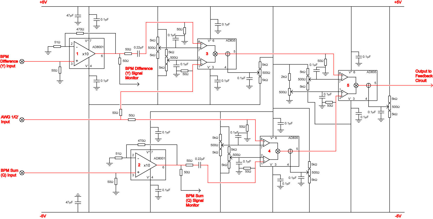
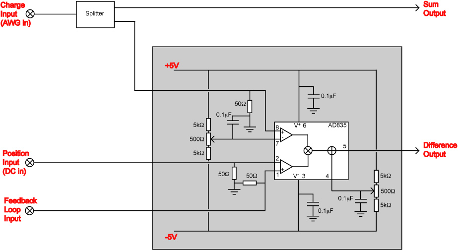
| Figure 5.24: A circuit diagram of the FONT charge normalisation circuit. For the purposes of the diagram, the difference signal is marked ‘Y’ and the sum signal marked ‘Q’ to denote the measurement extracted from each signal. The pin numbers of each chip are marked on the diagram; the signal path is marked in red. |
The normaliser circuit is, in many ways, the most important component of the FONT feedback electronics, since the signal manipulation that it carries out is the most intricate of all the FONT electronics. The aim is to take the BPM sum and difference signals and produce a normalised signal whose magnitude is a function only of the beam position at the BPM. As mentioned above, this is achieved by multiplying the difference signal by the inverted sum signal from the previous pulse. In addition, a first order correction is made by the normaliser to account for any difference between the sum signals of current and previous pulses. This first order correction is based around the first two terms of a Taylor expansion [30]:
| (5.12) |
where dΣ = Σ−Σ′ and the prime denotes the sum signal from the previous pulse. It is therefore possible, using this first order expansion, to correct for the difference in sum signals between the current and previous pulses. A circuit diagram of the normaliser circuit is shown in Fig. 5.24.
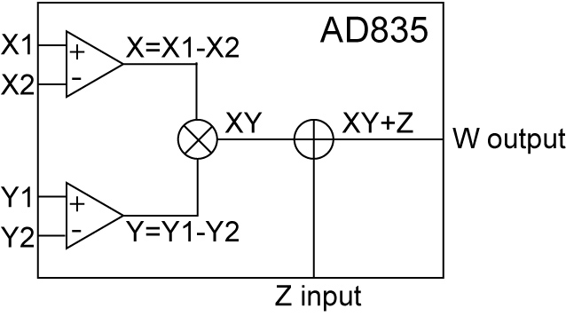
| Figure 5.25: Functional block diagram of the AD835 fast multiplier chip (adapted from [114]). |
The full signal normalisation, as given in Eq. (5.12), is achieved in the normaliser circuit with three fast multiplier chips, with an additional three amplifier chips used to set the signal voltages to the correct level. The three multiplier chips are Analog Devices AD835 250 MHz 4-quadrant multipliers (for details see [114]). A functional block diagram of the chip is shown in Fig. 5.25. The AD835 multiplier was selected for its high speed and bandwidth and low latency time [30]. The chip accepts four primary input signals (marked X1, X2, Y1 and Y2 in Fig. 5.25), with a fifth input (Z) used as an additional offset. It then produces at its output the product
The second multiplier chip (the ‘Sum Multiplier’, marked ‘4’ in Fig. 5.24) carries out the first part of the first-order correction given in Eq. (5.12). In fact, this computational procedure can be made simpler still, since:
| (5.13) |
The requirement of the second multiplier chip is therefore reduced to calculating Σ/Σ′. This is achieved in the same way as the Δ/Σ′ multiplication carried out by the previous AD835: the inverted sum signal from the previous pulse, 1/Σ′, is input at X1, with the current sum signal (Σ) input at Y1, giving an output XY = Σ/Σ′. As before, the signal inputs X2, Y2 and Z are used to cancel the voltage offsets inherent in the chip, using 3 variable resistor networks as described above (see Fig. 5.24).
The final multiplier chip (the ‘Normaliser’, marked ‘5’ in Fig. 5.24) carries out the second stage of the first order correction. The output from the first multiplier (Δ/Σ′) is input into X1, with X2 used to correct the inherent offset voltage of X1 and X2 in the same way as before. The Y inputs are then used for the first-order correction signal. In order to produce the required signal, the simplest way would be to input a constant 2 V signal at Y1 and the calculated Σ/Σ′ signal from chip 4 into Y2, giving Y = (2 − Σ/Σ′). However, the maximum signal input of each input of the AD835 is ~1.2 V [114]. As such, the signal level must be divided by 2: a constant 1 V signal is therefore input at Y1, with the signal at Y2 reduced to Σ/2Σ′. The resultant signal Y is therefore:
| (5.14) |
The 1/Σ′ signal from the AWG is split on the normaliser circuit board with a resistive splitter network. In this way,the required 1/2Σ′ signal is delivered to the second AD835 to produce the correct signal levels at the final multiplier. However, this in turn means that the output of the first multiplier is reduced by a factor of two, to give XY = Δ/2Σ′. As such, the output of the final multiplier chip is therefore:
| (5.15) |
as required by Eq. (5.13). As before, the Z input is used to correct for the inherent offset of the chip output with a variable resistor network, as described above. The output of the normaliser circuit is therefore, to a good approximation, dependent only on the position of the beam at the BPM and is now independent of the beam charge.
In order to correct for the factor of 4 reduction in signal level, as given in Eq. (5.15), an Analog Devices AD8001 Current Feedback Amplifier is used to amplify the output of the final multiplier chip [115]. The AD8001 high speed amplifier chip was selected, as with the AD835 multiplier, for its large bandwidth (800 MHz at unity gain [115]) and low latency time [30]. The AD8001 provides a maximum output voltage swing of ±3.1 V, for a maximum differential input voltage of ±1.2 V [115]. For the normaliser circuit, the amplifier is used as a simple non-inverting amplifier, with the inverting input grounded. A single AD8001 with a gain of 5 is used to amplify the output of the final multiplier chip up to the correct output voltage (chip is shown in Fig. 5.26 marked ‘6’ and is termed the ‘Normaliser Pre-Amp’)60. As with most operational amplifiers, the gain is set with a pair of resistors: an input resistor, Ri, connected to the inverting input, and a feedback resistor, Rf, connected between the inverting input and amplifier output. For a non-inverting input signal, the gain is defined as:
| (5.16) |
The stability, flatness and settle time of the AD8001 output is highly dependent upon the correct matching of Ri and Rf. By interpolation of the figures given in [115], the best match for a gain of 5 was achieved with Ri = 125 Ω and Rf = 511 Ω.
In addition to this output amplifier, two more AD8001's are used as signal pre-amplifiers for the Σ and Δ inputs of the normaliser circuit (chips are marked ‘1’ and ‘2’ in Fig. 5.24 and are referred to as the ‘Sum Pre-Amp’ and ‘Difference Pre-Amp’). These two amplifiers are used to amplify the raw sum and difference signals up to the correct voltages for processing by the multiplier chips. The maximum output of the X-band BPM processor is ~200 mV (see Section 4.8.2); however, the tolerances of the AD835 multipliers require an input voltage in the range 0.5 < Vin < 1 V for reliable chip operation [30]. As such, the two AD8001 pre-amplifiers are set with a gain of 10. The output signal is then split with a 50:50 resistive splitter network: half the signal goes to the AD835, with the other half output to 3/8-in. heliax to allow monitoring and measuring of the sum and difference signals and inversion of the sum signal with the FONT DAQ system. In addition, a 0.22 µF capacitor is connected in series between the output of the pre-amplifier and the input of each multiplier. The purpose of this decoupling capacitor is to remove the DC offset produced by each mixer in the BPM processor (see Section 4.6.2), while still allowing the signal from the BPM to pass unhindered.
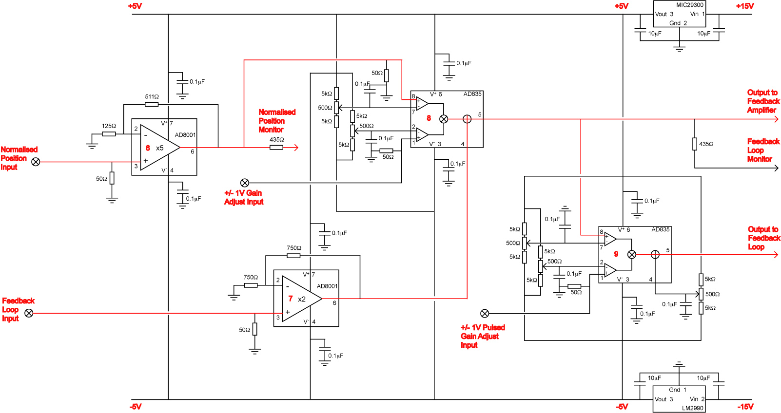
| Figure 5.26: A circuit diagram of the FONT feedback circuit. The pin numbers of each chip are marked on the diagram; the signal path is marked in red. |
The FONT feedback circuit is the part of the FONT electronics designed to replicate the Smith feedback design, as discussed in Section 3.2. The output of the normaliser circuit is first amplified to the correct level, then split in two. One half of the signal is sent to the kicker amplifier and is used to steer the beam (see Section 5.3.5). The other half of the signal is passed through a delay cable that has the same signal length as the latency of the entire system. The signal from the delay cable is then added to the output from the normaliser circuit and the whole process repeats for the duration of the beam pulse.
A circuit diagram of the feedback circuit is shown in Fig. 5.26. The feedback circuit consists of 3 chips, plus a fourth AD8001 amplifier (details given previously in Section 5.3.1). This amplifier chip (the ‘Normaliser Pre-Amp’, marked ‘6’ in Fig. 5.26) is used to amplify the normalised position signal up to the correct voltage. The output of the amplifier chip is then split with a 10:1 resistive splitter network to allow external monitoring of the normalised position signal. An AD835 multiplier is then used as a gain control for the normalised signal and to add the signal from the delay cable (the ‘Feedback Multiplier’, marked ‘8’ in Fig. 5.26).
The X1 input of the multiplier chip takes the normalised position signal; as before, a variable resistor network is connected to the X2 input to allow cancellation of the voltage offsets of the X inputs. Connected to the Y1 input is a ±1 V DC power supply, mounted outside the tunnel and run in on BNC cable. This allows remote adjustment of the normalised position signal before it reaches the kicker amplifier or delay loop; it also allows the sign of the signal to be changed remotely. The Y2 input is used as an offset voltage adjust as before. The signal from the delay loop passes into the Z input and is summed with the normalised position signal produced by the normaliser circuit. Since there is now no control over the offset voltage of the W output, an AD835 chip was selected with the smallest possible offset: for a correctly zeroed input, an output of less than 10 mV was measured.
The output of the feedback multiplier chip is then split a number of ways. The direct output is first sent along two paths: one passes through a second multiplier that sets the gain of the signal that travels around the delay loop (see below). The output of the chip is connected directly to the input of the second multiplier, rather than through a resistive splitter, since the short cable lengths involved do not introduce sufficient impedance to cause an impedance mismatch [43]. The second signal path then travels through another 10:1 resistive splitter network to allow monitoring of the feedback signal with the FONT DAQ system; finally, the feedback signal is output to the kicker amplifier.
The final multiplier chip used in the feedback circuit is another AD835 (the ‘Loop Multiplier’, marked ‘9’ in Fig. 5.26) that is used to control the gain of the signal that travels around the delay loop. It is used in the same fashion as the feedback multiplier chip, as detailed above, with the feedback signal for the delay loop input into the X1 input. The gain control is input into the Y1 input and, as with the feedback multiplier, is a ±1 V signal that allows remote adjustment of the magnitude and sign of the feedback signal. However, unlike the feedback multiplier, the loop multiplier gain control is pulsed: the gain pulse lasts only for 500 ns and is timed to switch on the loop multiplier chip for the duration of the beam pulse. Pulsing the loop gain serves the same purpose as the delay loop reset mentioned in Section 3.2.3. Without any sort of switch, the signal in the delay loop would quickly run away to infinity (or, in the case of the FONT feedback circuit, rapidly saturate the multiplier chips) due to the iterative summing carried out by the feedback multiplier: as such, the gain pulse switches off the delay loop signal after 500 ns, preventing the signal from saturating. A square pulse generator with a remote trigger input was used to provide the pulsed gain control.
The final chip on the feedback circuit is another AD8001 amplifier (the ‘Feedback Pre-Amp’, marked ‘7’ in Fig. 5.26). This amplifier is connected between the signal return of the delay loop and the Z input of the feedback multiplier. The purpose of this feedback pre-amp is to amplify the signal that comes out of the delay loop: since there are signal losses inherent in any length of cable, it is necessary to rectify these signal losses with a ×2 amplifier to bring the signal back up to the required level. The precise output of the delay loop can then be set with the gain of the loop multiplier.
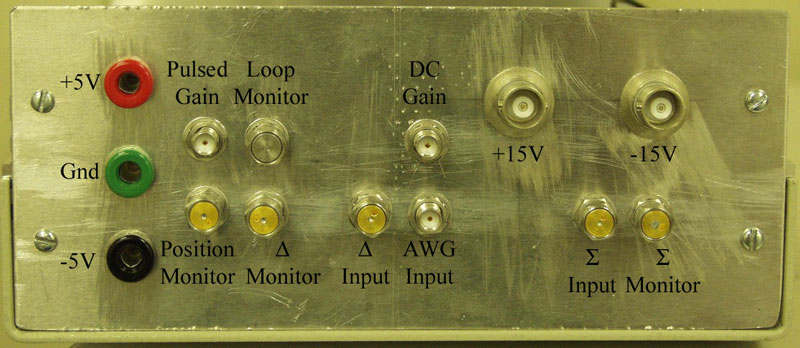
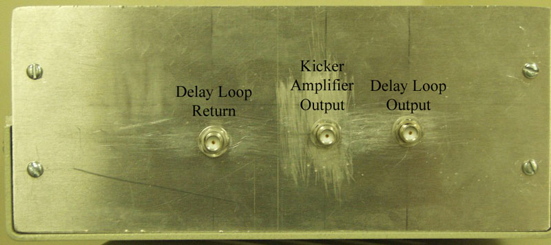
| Figure 5.27: The complete FONT feedback and charge normalisation circuit: the signal and power supply inputs are all on the left, with the two normalised outputs on the right hand side with the delay loop signal return (see Fig. 5.28). The red and black wires are the positive and negative 15 V power supplies respectively. |
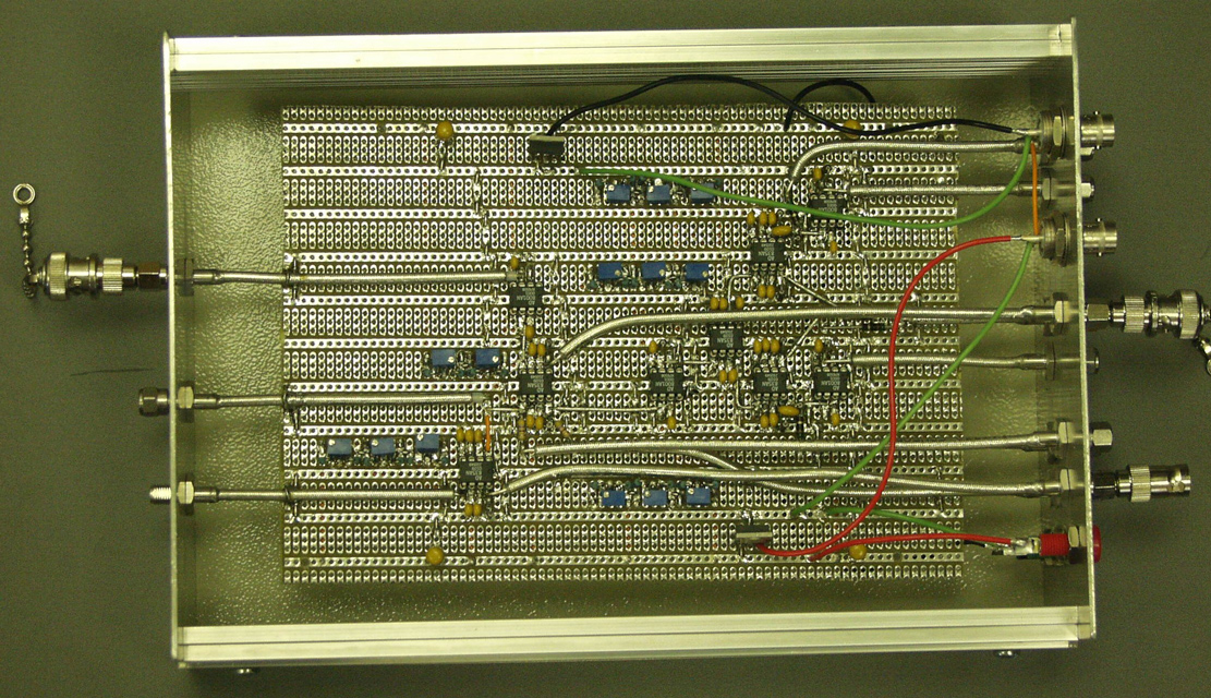
The entire feedback circuit was fabricated on a single circuit board with the normaliser circuit: the complete circuit can be seen in Fig. 5.27. Integrating the two circuits onto a single board allows minimisation of signal losses and, more importantly, the reduction in signal delay between components. The entire signal path between components was assembled from 1/32-in. (0.08 mm) coaxial cable to ensure optimum signal speed and impedance matching. The coaxial cable also provides a degree of shielding from external RF interference. The circuit board was mounted within a rigid metal box: the input and output signals were connected to SMA bulkhead connectors on the front and rear panels with 1/8-in. (0.32 mm) coaxial cable (see Fig. 5.27). Power was supplied to the board with two BNC connectors mounted on the front panel. The full connector layout of the front and rear panels is shown in Fig. 5.28. An additional set of ±5 V connectors was assembled on the front panel of the board, taking power from the board itself, to allow the connection of any additional external amplifiers.
|
|
||||
| (a) Front panel | (b) Rear panel | ||||
|
|||||
All of the chips used in the feedback and normaliser circuit require a voltage supply of ±5 V. An external voltage supply of ±15 V is supplied to the board via 2 BNC cables. A Micrel Electronics MIC29300 low dropout regulator is used to drop the +15 V supply voltage to the required +5 V for the chip power supplies [116]; a National Semiconductor LM2990 negative low dropout voltage regulator is used to limit the negative supply at −5 V [117]. In order that the voltage supplies could cope with the demands of the rapid signal variation of the FONT BPM pulses, 10 µF capacitors were connected between ground and the input and output terminals of both voltage regulators. The purpose of these capacitors is to allow current to be drawn rapidly from the capacitors, before the power supply has had time to react, and keeping the power supply to each chip uninterrupted. For the same reason, a pair of 47 µF capacitors was connected between each power supply rail on the circuit board and ground, one at each end of the board. In addition, a 0.1 µF tantalum capacitor was connected between ground and both power supply pins of each chip, again to provide a rapid current source.
As mentioned previously, there is an inherent DC offset present on each of the signal pins of the AD835: in each case, a variable resistor network was used to cancel the effect of these voltage offsets. To facilitate accurate cancellation of these offsets, a systematic trimming procedure, proposed by Josef Frisch, was followed once the circuit had been fabricated: this trimming procedure is detailed in Appendix A.
The data acquisition system for FONT is similar to that already mentioned at the beginning of Section 4.7. Two Tektronix TDS684C 1 GHz four channel digitising oscilloscopes [118], each with a sampling rate of 5 Gs/s, provided the front end of the DAQ system, giving eight available DAQ channels. Four channels were required for the four monitor signals output from the feedback circuit: the raw BPM sum and difference, the normalised position and the feedback loop signals (see Figs. 5.24, 5.26 and 5.28(a)). As a corroborative measurement of the accuracy of the BPM sum signal, the output of Toroid 1750 was recorded; the voltage applied to the kicker magnet was also recorded using the same 100:1 pickoff arrangement as before (see Section 5.2.4). A seventh channel was used to measure the output of the signal generator used to produce the pulsed gain signal, to allow the timing to be measured and adjusted. Finally, the output of the AWG, used to produce the inverted charge signal, was recorded (see below).
The two oscilloscopes were set up outside the NLCTA tunnel: all the necessary cabling was run out of the tunnel through two ports in the roof, above quads QD1130 and QD1810 (see Figs. 5.1 and 5.2). This cabling consisted of six 3/8-in. heliax cables for each of the monitor signals and the AWG signal input, plus four BNC coaxial cables used to carry the two gain signals and the ±15 V power supply voltages. An Agilent E3630A DC power supply [119] was used to provide both the ±15 V supplies to the board and the DC gain voltage. A custom built rack mount splitter board, also situated outside the tunnel, was used to distribute the ±15 V from the power supply, with a variable resistor network used to supply and control the DC gain61.
Both scopes were connected via GPIB to a GPIB-to-TCP/IP network interface box: this allowed remote control of the scopes over TCP/IP using the GPIB protocol. A PC in the NLCTA control room was configured to be able to address the TCP/IP box over the existing NLCTA local area network. The PC was set up to control the scopes using the GPIB commands in Matlab: this allowed the complete integration of the FONT DAQ and data analysis, as well as easy data storage for offline analysis in the standard Matlab file format. A number of Matlab routines were written by Gavin Nesom to allow full GPIB control and DAQ of the scopes, providing a fully automated DAQ procedure. A number of subroutines were written to control the setup of the scopes (timebase, trigger, channel selection etc.) and the DAQ procedure, allowing easy adjustment of the various setup parameters. Also included was a subroutine to allow control of the AWG via GPIB (see below).
Both scopes were set up to use a common external trigger. This trigger pulse was provided by the NLCTA BPM micro TA02 responsible for acquiring data from the downstream end of the NLCTA62. As such, the scopes were set to acquire data at the same time as the NLCTA BPM's. This had the added advantage that the NLCTA BPM's had to be set up to acquire data whenever FONT was running so that the correct trigger signal could be provided for the scopes, meaning that it was a trivial process to collect data from the NLCTA BPM's with the SCP at the same time as FONT. The scopes were set up to acquire a single set of data: the Matlab routine would then retrieve that data from the scopes whenever they entered this “stopped” state. Once the DAQ process for a single data pulse had been completed, the scopes would be reset to the “single acquisition” state and the process would repeat. In this way, it was possible to ensure that the scopes would trigger only when the Matlab routine was ready to record the data.
Having acquired and recorded the data from a single pulse, the next stage is to calculate and output the inverted sum signal (1/Q) to the feedback circuit. An Agilent 33250A 80 MHz Arbitrary Waveform Generator (AWG) [120] was used to provide the inverted sum signal. An arbitrary waveform generator (or AFG: arbitrary function generator) is a signal generator that can be programmed to output any desired waveform, up to its bandwidth limit. The 33250A AWG is equipped with GPIB, to allow remote programming of the arbitrary waveform, and a dedicated trigger input. The trigger input allows the AWG to be programmed with the required waveform, which is then output whenever a trigger pulse is received. It is also possible to program in a delay time — up to 85 s and with 0.1 ns resolution — between the unit receiving the trigger pulse and outputting the desired waveform: this allows remote adjustment of the time at which the arbitrary waveform is output. This trigger delay, along with the AWG output mode and frequency, is programmed into the AWG as part of the initial setup subroutine of the DAQ program in Matlab. In truth, the bandwidth of the AWG arbitrary waveform output is limited not only by the 80 MHz bandwidth of the output, but also by the maximum sampling rate of the input waveform of 200 MHz, giving a maximum granularity of the inverted charge signal of 5 ns. However, it was felt that this provided sufficient bandwidth to produce an acceptable signal output [30].
Once the BPM data has been acquired and stored by Matlab, the inverted sum signal is calculated from the recorded BPM sum signal. A limit is placed on the magnitude of the inverted signal in software to prevent the AWG output going over 2 V: this keeps the signal input to the two first stage multiplier chips on the feedback board below the required 1 V signal maximum. If this limit was not put in place, the inverted signal would rapidly diverge to infinity as the sum signal drops away rapidly at the start and end of the pulse, overloading the signal inputs to the normaliser circuit. Once the inverted signal has been calculated, it is then sent via GPIB to the AWG. The AWG then outputs this waveform to the feedback circuit via a 3/8-in. heliax cable, as mentioned above, which carries the signal into the tunnel. The trigger for the AWG is provided by a separate crate on TA01, allowing the AWG waveform to be output prior to the beam reaching the FONT BPM. The exact timing of this trigger is then controlled using the trigger delay within the Matlab DAQ routine.
The final stage of the DAQ process is to save the recorded data to disk. The DAQ routine is set to run for a preprogrammed number of pulses: during each pulse, the data for that pulse is recorded in the Matlab workspace with a unique variable name. Once all the pulses have been recorded, the data for each pulse is recorded in a single .mat-file: this records the time and voltage information for each scope channel, plus the calculated inverted sum signal. The full DAQ program therefore encompasses the following subroutines:
As mentioned previously, at the end of Section 5.3.1, the reliable input voltage range for the AD835 multipliers used in the normaliser circuit is limited to 0.5 < Vin < 1 V. This limits the output of the sum and difference signals of the BPM processor to 0.1 < Vout < 0.2 V: this not only places a constraint on the peak output of the processor, but also on the flatness of the BPM signal i.e. the flatness of the charge distribution within the pulse. Independent of the absolute magnitude of either the sum or difference signals, it is a necessary condition that the charge distribution within the pulse not vary by more than a factor of 2 within the measurable portion of the pulse. This means that droops in the sum signal, such as those seen in Fig. 4.49, are unacceptable. Removal of these dips in the charge distribution was doubly important since such droops are thought to be the cause of the overshoot seen on the BPM difference signal (see Section 4.8.3 for details). It was therefore necessary to ensure that the beam was tuned to such a standard that such droops were not seen in the final FONT runs.
| Figure 5.29: Circuit diagrams of each of the stages in the FONT BPM signal pre-amplifiers [43]. Each pre-amp contains 3 of the 12 dB amplifier stages, plus one 6 dB and one 3 dB stage; the resistor networks ensure correct 50 Ω impedance matching for each stage. This also means that the gain of the amplifier is cut from ×8 to ×4. |
However, it was felt that, in order to limit the absolute magnitude of both the sum and difference signals to ±200 mV, a signal pre-amplifier should be used between the output of the BPM processor and the input to the normaliser circuit [121]. A pair of pre-amplifiers was designed and built by Colin Perry, based around the same AD8001 amplifier as used in the feedback circuit. Each pre-amp circuit provided an adjustable gain range between −9 dB and +36 dB in 3 dB steps. Each circuit consists of 3 gain stages and 2 attenuator stages: the circuit diagram of each of the stages is shown in Fig. 5.29. The attenuator section in each stage is remotely switchable via a series of relays, controlled from outside the tunnel via a custom-built multiple strand cable and selector switch. The cable also provides power for the six amplifiers in the circuit. Each amplifier is set always to be on: in this way, the signal delay through the entire pre-amplifier is independent of the gain selected. These pre-amplifiers therefore provided a method of remotely adjusting the voltage of the sum and difference signals output by the BPM processor.
In addition to the BPM pre-amplifiers, a remote method of adjusting the length of the delay loop was also discussed [121]. A delay box featuring a second relay assembly, with four relay stages, was designed and built by Colin Perry, making use of the same cable used to control the BPM pre-amps. This relay assembly follows a similar design to that of the 3 dB stage of the pre-amps shown in Fig. 5.29. However, the resistor network is replaced with a pair of external BNC connectors, allowing a BNC cable to be connected. The delay box is then placed in series with the delay cable, allowing the remote adjustment of the latency of the delay loop. The four external cables allow an additional delay of up to 42 ns to be added to the delay loop, allowing the latency of the delay loop to be remotely adjusted with a granularity of ~2.5 ns.
The FONT kicker amplifier is, from an electronics perspective, the most complex part of the entire FONT system. It was also the component that required the most intensive R&D to achieve the required signal output. A kick voltage of some 300 V is required for the kicker magnet to produce a modest position change of 1 normalised BPM Unit (see Section 5.2.3) — this corresponds to a power output of around 2 kW, for a rise time less than 5 ns. The equivalent requirement for the actual IPFB kicker driver is a maximum power output of 10 W (see Section 3.2.3). It was not possible therefore to use the design intended for use with the IPFB system for FONT, since the power requirements are so much greater [56].
|
|
||||
| (a) Planar triode | (b) Triode tube diagram | ||||
|
|||||
As such, a new amplifier design had to be conceived in order to deliver the high power, low rise time requirements of the FONT system. Such an amplifier was designed and constructed by Colin Perry at Oxford University. This amplifier design is based around three Y690 planar triode tubes, which are used to amplify the incoming signal from the feedback circuit and power the signal that is used to drive the kicker magnet. The Y690 tube used for FONT is shown in Fig. 5.30, along with its circuit diagram. The planar triode is a particular type of tube designed for use at both high frequency and power [43]: it differs from a standard tube in that the internal connections — heater, cathode, grid and anode — are arranged parallel to one another in a planar arrangement, hence the name [123]. Otherwise, the planar triode operates in the same fashion as any other tube. A heater is used to heat a cathode and boil off electrons: these are accelerated towards an anode by a potential difference applied between cathode and anode. A modulating signal is applied to the grid, which controls the electron flow between cathode and anode: as such, the signal on the grid is amplified at the anode. The amplified signal is therefore picked off at the anode; the gain of the tube depends upon the applied bias voltage between cathode and anode.
The planar triode is normally used to amplify high frequency signals with a high output power. By decreasing the gap width between cathode, grid and anode, the electron drift time is reduced, increasing the bandwidth of the tube [122]: the Y690 can amplify signals up to 2 GHz [124]. However, it is not possible to make the planar triode too small, due to the large amount of heat generated during high power operation: this sets a limit on the size of the tube and therefore on the maximum output frequency [43].
| Figure 5.31: The electronics layout within the FONT kicker amplifier. The three planar triodes are encased within the black heat sinks in the centre of the box. The feedback signal and trigger inputs are on the right hand end of the box, with the high voltage supply input and kicker supply output on the left. |
As mentioned above, the Perry design for the FONT kicker amplifier makes use of three Y690 planar triodes to amplify the signal from the feedback circuit and drive the kicker magnet. The completed amplifier is shown in Fig. 5.31. The amplifier has a small pre-amp stage that amplifies the ±1 V output of the feedback circuit up to ±5 V. This ±5 V signal is then amplified again to the ±350 V signal used to drive the kicker magnet. The amplifier is designed to sit as close to the kicker as possible, and is connected to the kicker signal input with 1/2-in. heliax (see Section 5.2.3).
In addition, the amplifier has two external control boxes that sit outside the tunnel. The first provides the high voltage power supply that is used to power the tubes: this is brought into the tunnel on HV BNC cable. The second control box provides the trigger for the main amplifier. The amplifier operates by modulating the output pulse that is produced by the tubes when the bias voltage is first applied and the anode current begins to settle. Since the tubes must be powered on before the beam pulse arrives, this bias voltage must be applied in time for the beam pulse to arrive. As such, the amplifier uses a separate trigger to switch the tubes on around 3 µs before the arrival of the beam pulse. The trigger pulse is supplied to the amplifier from the control box via a 37-pin connector and cable that connects to the front of the control box. The two external control boxes are shown in Fig. 5.32.
Prior to installation of the FONT electronics inside the NLCTA tunnel, it was felt that a full system bench test would be vital in checking the correct operation of the system. As such, a tester circuit was designed by Josef Frisch and assembled by Tonee Smith at SLAC to provide simulated BPM difference and sum signals for the feedback circuit. The tester circuit was designed to recreate the sum and difference signals produced by the FONT BPM processor (see Section 4.6) and is described in Section 5.4.2. In order to do so, it was necessary to simulate the beam position and charge as seen by the BPM.
The simplest source of data for recreating the charge and position of the beam was the large quantity of previously collected BPM data. Using one of these many datasets would allow a large range of position and charge signals to be input to the feedback circuit, all from real measurements. A pair of Stanford Research Systems DS345 30 MHz Arbitrary Waveform Generators [125] was utilised to output these faked beam signals. The DS345 operates in the same fashion as the Agilent 33250A AWG used to produce the inverted sum signal. Each AWG can be programmed with an arbitrary waveform, with a specified frequency and magnitude, and output either at a predetermined time interval or in response to an external trigger signal. As such, it was possible to program one of the DS345's with a facsimile of the beam position and another with the beam charge.
As with the 33250A, the DS345 can be controlled through its GPIB interface. Although this gave the possibility that the DS345's could be programmed using the same Matlab GPIB routines used for the DAQ system, this could not be achieved in the short time available. As such, a series of LabView VI's used to control the DS345, written by Kirsten Hacker at SLAC, were modified for FONT's purposes by Tonee Smith and Stephen Molloy. These allowed each of the DS345's to be programmed with the specified charge and position waveforms. Each waveform could be selected from amongst a large set, allowing LabView to cycle through the set and provide a position and charge variation from pulse to pulse, rather than simply using the same pulse shape repeatedly.
LabView, however, requires data files in a different format than Matlab: tab-delimited .dat files as opposed to Matlab's proprietary .mat format. In order to provide LabView with the necessary waveforms, a selection of data from a previous run was converted to .dat format for use in LabView by Gavin Nesom. Since the BPM sum signal is an excellent measurement of the true beam charge (see Section 4.8.1), in each case the BPM sum signal was used to produce the beam charge waveform. For the beam position waveform, the normalised beam position was calculated using the recorded sum and difference signals, with the intention that the tester circuit should simply reverse this procedure (see Section 5.4.2). Both waveforms were then scaled to 1 V maximum amplitude.
|
|
||||
|
|||||
However, having produced these simulated position and charge signals, it quickly became clear that the DS345 AWG's would be unable to reproduce these waveforms with the required granularity. The DS345 has an output bandwidth of 10 MHz for an arbitrary waveform, with a maximum sampling rate of 40 MHz: this corresponds to a minimum point spacing of 25 ns. As such, any features in the charge and position profiles shorter than around 50 ns in length would not appear on the simulated waveforms. The output of the DS345, using a real charge profile for the arbitrary waveform input, is shown in Fig. 5.33. This gave two possibilities:
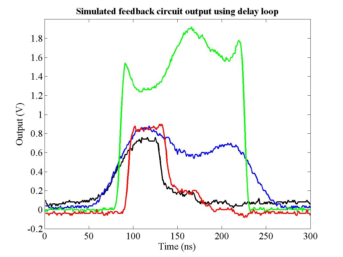
Given that one of the main constraints on the real system was the limited beam pulse length of some 180 ns, it was felt that lengthening the simulated pulse would not gain anything for the simulation. Since neither case would be able to simulate the rapid charge variation seen on the real pulse (see Fig. 4.51), increasing the pulse length would only have further weakened the accuracy of the simulation. As such, it was also feasible to produce a number of position waveforms with flat or tilted profiles, without the detailed structure seen in the real beam, to provide some simpler cases for study. A selection of the simulated beam charge and position profiles is shown in Fig. 5.35 at the end of Section 5.4.3.
The purpose of producing simulated position and charge signals, as opposed to sum and difference signals, is that, although the feedback circuit requires the BPM sum and difference signals as its inputs, the corrective output signal is given in terms of the beam position i.e. a voltage to be amplified and applied to the kicker magnet, which causes a change only in the beam position. Since one is attempting to feed the output of the feedback circuit back to the input to replicate the effect of the kick applied to the beam, it is simpler to do this in terms of the beam position (multiplying position and charge to produce the difference signal) than the BPM difference signal (dividing difference by sum to give beam position). As mentioned previously, a tester circuit was fabricated to simulate the signal output of the beam components that are not present for the bench test i.e. the BPM sum and difference signals produced in response to the FONT system correction.
| Figure 5.34: Circuit diagram of the FONT feedback tester circuit. The charge signal passes through the splitter and is output as the sum signal; the multiplier chip uses the position and charge signals to produce the difference signal. The corrective output from the feedback circuit is summed at the position input. |
A circuit diagram of the tester circuit is shown in Fig. 5.34. The circuit is constructed around the same AD835 multiplier chip used for the feedback circuit. The power supply for this tester circuit was provided by the ±5 V connections on the front of the feedback box. The tester circuit takes the two simulated position and charge signals produced by the DS345 AWG's as its inputs. The charge signal is first split using a resistive splitter network: half the signal goes straight to the sum input of the feedback circuit to simulate the sum signal. The other half is used by the tester circuit to produce the simulated difference output. The charge signal is input to the X1 input of the AD835; the X2 input is used to correct the mutual voltage offset of the two inputs in the same manner as the other AD835's used in the feedback circuit (see Section 5.3.1 and Fig. 5.25 for details of the pin arrangements of the AD835 chip). The Z input also serves the same purpose, acting as an offset adjust for the voltage offset of the Z input and W output63.
The simulated position signal is input at Y1: with this setup, the signal seen at the output of the chip would therefore be the product of position and charge, which is, to a good approximation, the BPM difference signal. However, this setup would not include the corrective effect of the feedback circuit. Therefore, the output of the feedback circuit that would normally go on to the kicker amplifier is input to the Y2 input of the AD835. Since the kicker amplifier should have a linear input-output response, the amount that the beam is kicked by the kicker — and therefore deflected at the BPM — has a linear dependence on the output of the feedback circuit. As such, it is perfectly acceptable for the purposes of the simulation to have the output of the feedback circuit directly affect the simulated beam position. It is then possible to vary the magnitude and direction of this change in beam position by varying the sign and magnitude of the DC gain input to the feedback circuit.
In this way, the tester circuit simulates the effect of the feedback circuit correcting the position of a misaligned beam. The output of the feedback circuit is connected to the feedback loop input of the tester circuit via a 32 ns long BNC cable, to simulate the round trip time of the real FONT system. Initially, the same trigger signals as described in Section 5.3.3 were used for the FONT 33250A AWG and the scopes, to allow the feedback circuit to operate as closely as possible to the real beam test. In order to synchronise the test AWG's to the feedback circuit and AWG, the trigger output of the 33250A was used to trigger the two test AWG's.
A problem occurred with the initial setup of the triggers, since the test AWG's could only be synchronised to their 10 MHz clocks: although they would receive the trigger input from the 33250A at the correct time, the output would be delayed until the next clock cycle. This meant that the output of the test AWG's would not arrive at the same time for consecutive pulses within the acquisition window of the scopes. As such, the inverted signal produced by the 33250A would no longer align correctly with the simulated sum and difference signals due to the timing jitter. The eventual solution was to lengthen the output pulse of the position AWG to 500 ns, arriving before the start of the charge pulse. The FONT AWG and oscilloscopes were then set to trigger on the trigger output of the charge AWG, allowing all the components to be synchronised on each pulse.
Before the feedback circuit was tested with the simulated beam pulses, a series of measurements was made on the signal propagation delay of each component in the feedback circuit. A 500 ns 500 mV square pulse was input to the sum, difference and AWG inputs of the normaliser circuit: the sum and difference inputs each had a 14 dB attenuator connected in series to drop the input voltage to 100 mV. The signal path between the pulse generator and the AWG input was the shortest, allowing measurements to be made on the leading edge of the sum and difference pulses. With a ~700 mV DC signal input to the DC gain, the output of the circuit was measured to be ~400 mV, with a pulse length roughly the same as the input pulses.
| ||||||||||||||||||||||||||||||||||||||||||||||||||||
| ||||||||||||||||||||||||||||||||||||||||||||||||||||
The signal delay through each component was measured by using a scope probe at the input and output pins of each chip in the signal path. The half height voltage of the square pulse was used to measure the time difference between the reference point — the input of the difference pre-amp — and the measurement point. The signal delays for each component are summarised in Table 5.2. It is interesting to note that, although the signal delay through each of the AD835's is constant at around 1.7 ns, the delay through the AD8001's appears to be gain dependent, since the ×5 amplifier is almost half a nanosecond faster than the two ×10 amplifiers. This is consistent with the gain dependent bandwidth specifications of the chip [115]. The full circuit delay was measured to be 10.5 ns between the external SMA connectors of the difference input and the feedback output.
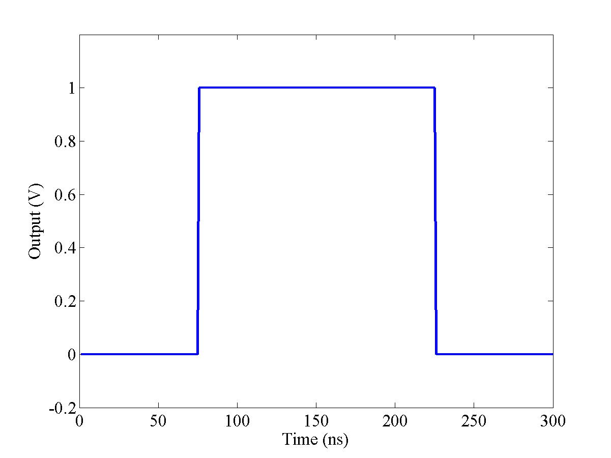
|
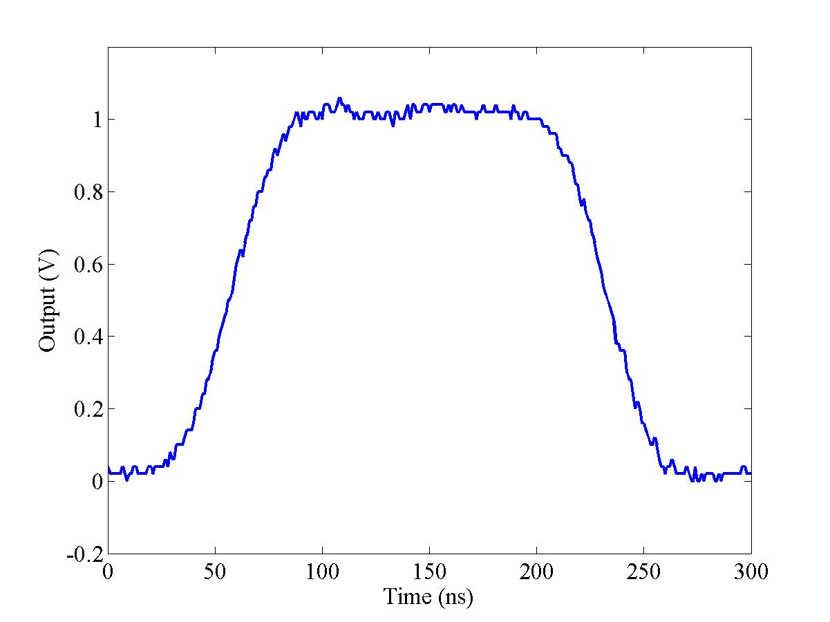
|
||||
| (a) Flat charge distribution | |||||
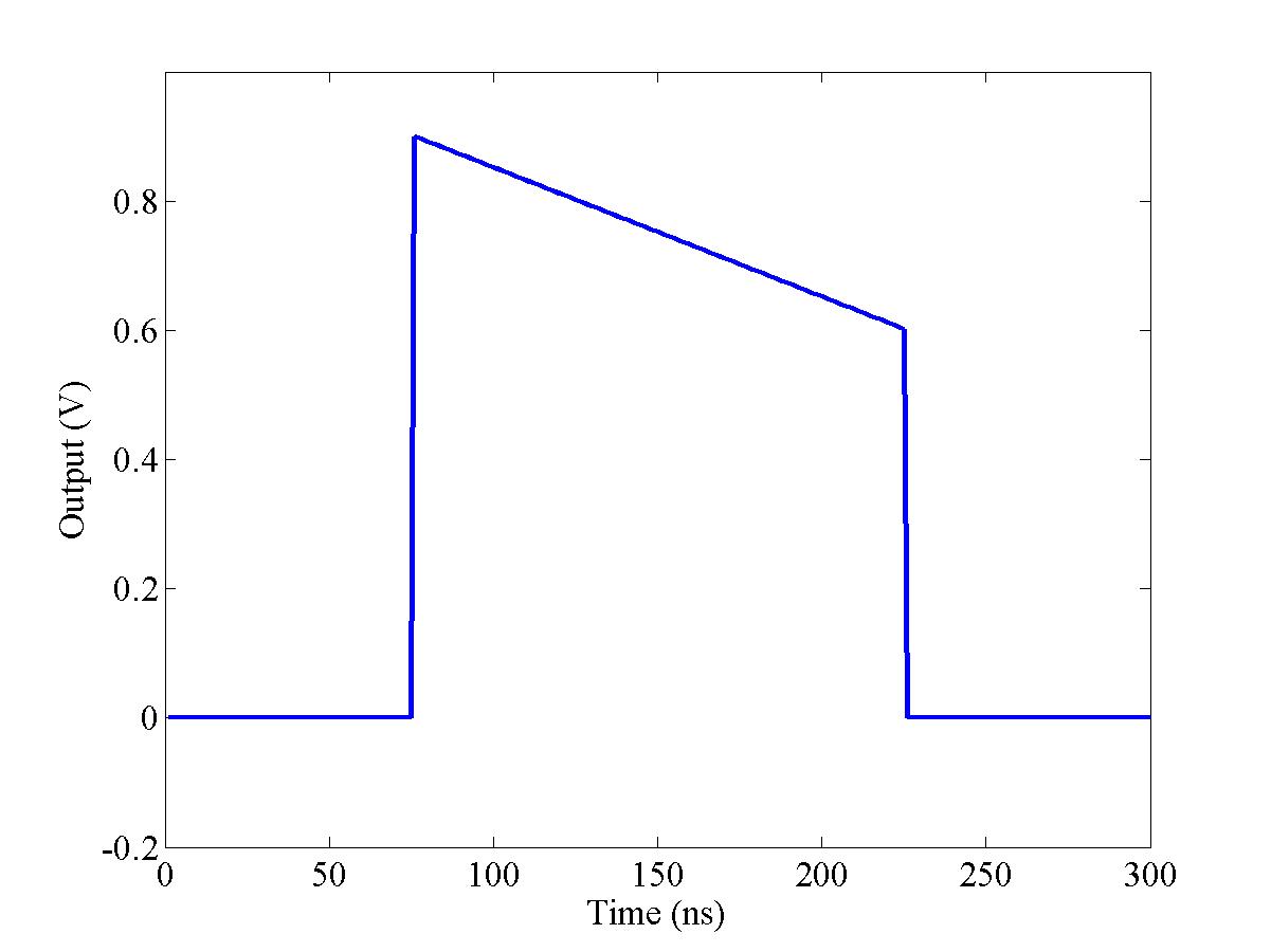 |
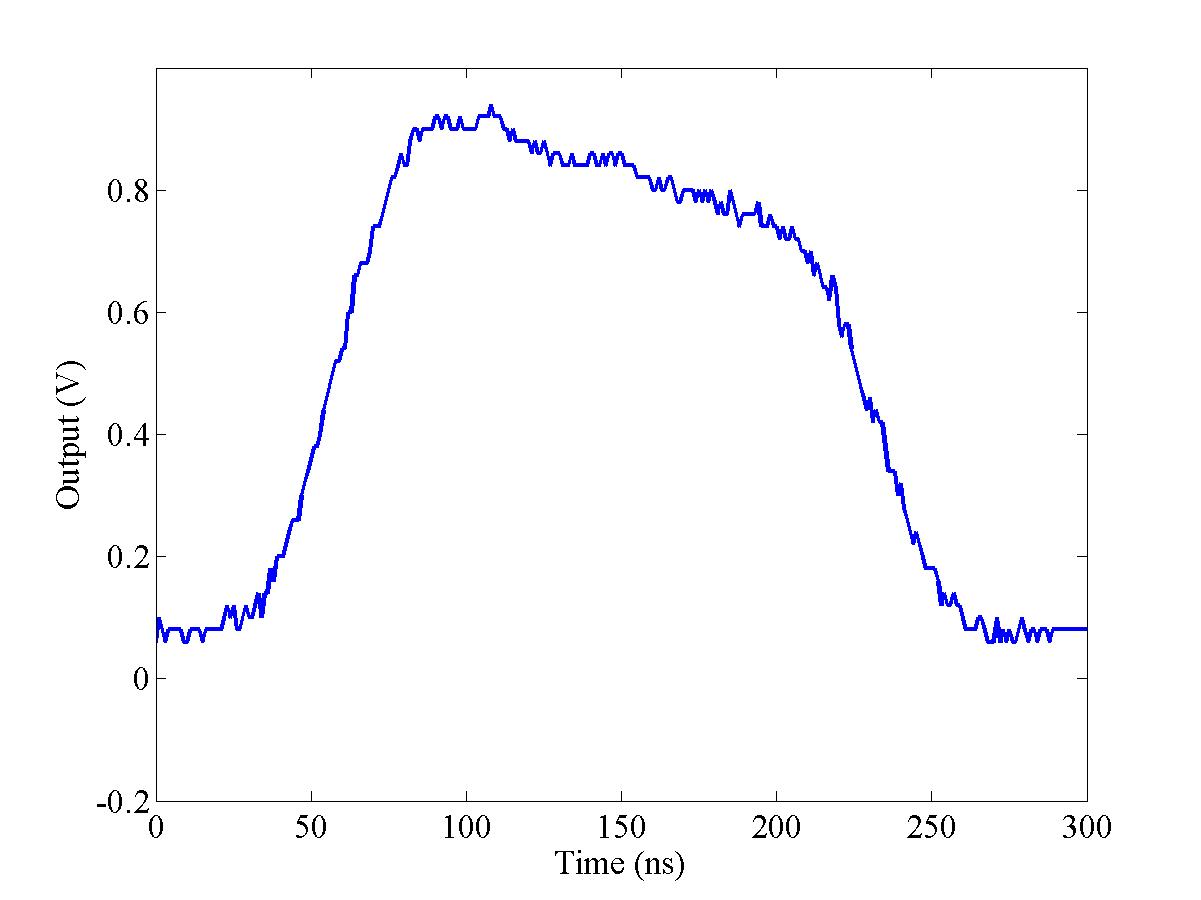 |
||||
| (b) Tilted charge distribution | |||||
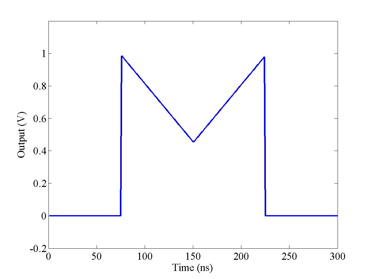 |
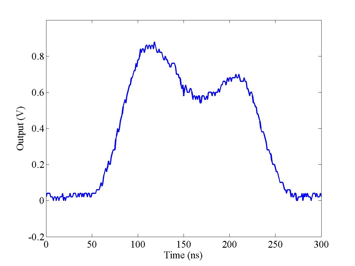 |
||||
| (c) Realistic charge signal | |||||
|
|||||
The full bench test of the feedback circuit was carried out in two parts: firstly without, and then with the delay loop. In both cases, the types of input pulse used were the same: the charge input signals are shown in Fig. 5.35. It is clear to see the effect of the bandwidth limit applied by the DS345 AWG: each of the pulses shown in Fig. 5.35 shows a significant smoothing between the input and output waveform of the DS345 (this is the reason for the shape difference of the two pulses shown in Fig. 5.35(c)). It is for this reason that these manually created charged distributions were used for a number of the tests. Since the complex charge variation seen on the real beam charge distribution is not repeated with the AWG pulse (see Fig. 5.33), the fake charge distributions allow a greater degree of manipulation of the signals input to the feedback circuit.
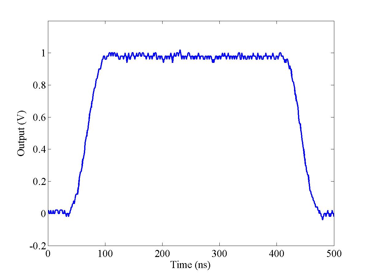
|
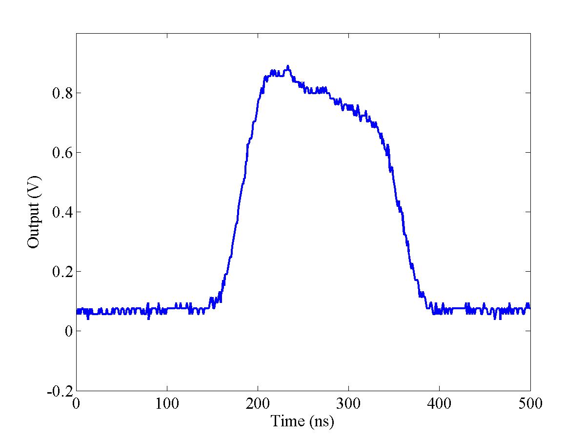
|
||||
| (a) Position signal | (b) Difference signal | ||||
|
|||||
The corresponding position signal is shown in Fig. 5.36(a): note that, as mentioned above, the position signal is considerably longer than the various charge signals shown in Fig. 5.35. The position signal was timed to arrive at the tester circuit some 100 ns before the charge signal. Using the charge profile shown in Fig. 5.35(b), the resultant difference signal output of the tester circuit (without the feedback circuit) is shown in Fig. 5.36(b). Since the position signal is essentially a 450 ns square pulse, the difference signal carries the shape of the charge signal, in a similar manner to the true sum and difference signals shown in Fig. 4.53.
| Figure 5.37: The output of the feedback circuit for the simulated beam charge profile shown in Fig. 5.35(a). The signals shown are: simulated sum signal (blue), simulated difference signal (black), FONT AWG 1/Q output (green) and feedback circuit normalised output (red). |
The resulting output of the feedback circuit, without the use of the delay loop, is shown in Fig. 5.37. The sum signal measured by the feedback circuit (blue) follows the expected profile. The FONT AWG signal (green) is clearly an inversion of the sum signal. The rapid cutoff that occurs at either end of this signal is a result of the limit that prevents the AWG signal from going over 2 V, as mentioned in Section 5.3.3. The AWG pulse sets the maximum length of the beam pulse that the feedback circuit processes: in this case, this is 180 ns.
The difference signal (black) exhibits the behaviour that one would expect from the circuit without the delay loop in operation. Initially, it follows the contour of the sum signal. At 100 ns, the effect of the offset has been measured by the feedback circuit, and a correction attempted. At this point, the simulated beam is steered down, towards the BPM ‘centre’, and the simulated difference signal drops accordingly. After another latency period, at 145 ns, the corrected beam has been registered by the feedback circuit: since the delay loop is not connected, the system has no memory of its previous correction and the difference signal (and beam position) returns to its previous level, essentially setting the system back to its initial state. After a further latency period, at 190 ns, the feedback circuit has once again measured the simulated beam offset and applied a correction to the beam position, which is reflected in the difference signal. Finally, at around 230 ns, the AWG 1/Q pulse switches off, preventing the feedback circuit from applying any further correction: the difference signal then returns to follow the sum signal as it drops back to zero.
The normalised output of the feedback circuit is shown on Fig. 5.37 in red. In some sense, this is the most important indicator of the health of the feedback circuit, since it is an indicator of where the feedback circuit thinks the beam is. The primary feature of the normalised signal is that it has roughly the same shape as the difference signal. More importantly, however, the normalised signal a) is clearly gated by the AWG pulse, since it rises sharply at 65 ns, and b) does not share the pulse shape of the sum signal at its leading or trailing edges. This can be seen clearly on the leading edge of the normalised signal: instead of showing the slow rise of the difference signal, the normalised signal has a sharp edge and plateau, indicating that the beam position is flat. It is possible to see the 11 ns latency of the feedback circuit: this is the cause of the delay between the black and red traces.
Also clear from the normalised signal is the cumulative effect of the bandwidth limit of each of the components of the feedback circuit. Although the normalised output shows a sharp leading edge, the rising and falling edges of the pulse become consistently slower with consecutive latency periods. This is likely to be caused by the limited bandwidth of the normaliser and feedback stages of the circuit, and results in a continuous smoothing with each successive pass round the feedback loop. This smoothing is likely to be exaggerated slightly by the AD835 used as part of the tester circuit and the 32 ns-long coaxial cable connected between the output of the feedback circuit and the feedback input of the tester circuit.
| Figure 5.38: The output of the feedback circuit for the simulated beam charge profile shown in Fig. 5.35(b). The signals shown are the same as those of Fig. 5.37. |
| Figure 5.39: The output of the feedback circuit for the simulated beam charge profile similar to that shown in Fig. 5.35(c). The signals shown are the same for those of Fig. 5.37. |
| Figure 5.40: The output of the feedback circuit for the simulated beam charge profile similar to that shown in Fig. 5.35(c) but with the addition of the delay loop. The signals shown are the same for those of Fig. 5.37. |
Both the initial normalised signal flatness and the signal smoothing can be seen on the normalised signal in Figs. 5.38 and 5.39: these show the same data as Fig. 5.37, but with two different charge profiles. Both the normalised position and the difference signals show the same general shape as seen in Fig. 5.37, but the effect of the altered charge profile can be seen on the difference signal and AWG output. The relative height of the peaks in the normalised signal is also similar between each of the three charge profiles. However, the dip in the signal after ~120 ns and the second peak at ~180 ns both show a small spike on the trailing edge. It is interesting to note that similar features also appear in the original IPFB simulations shown in Fig. 3.21. It was not possible, in the short time available, to fully establish the cause of these spikes. It is likely, however, that the feedback circuit is operating as designed, since the deviations between the normalised signals of Figs. 5.37-5.39 are small.
The next stage in the bench test was to include the feedback loop. The variable delay loop control, described in Section 5.3.4, was also included, to allow accurate adjustment of the length of the delay loop. Using the charge profile shown in Fig. 5.35(c), the output of the feedback circuit is shown in Fig. 5.40. Again, the sum signal (blue) shows the double peaked shape seen previously, with the AWG 1/Q signal (green) clearly the inversion of this signal, with a cutoff at around 2 V. However, when compared with Fig. 5.39, the difference and normalised position signals now clearly show the effect of the delay loop. After the second latency period, instead of rising back to the original level, both signals now continue to step towards zero, indicating that the simulated beam is being slowly steered back towards the centre of the BPM.
| Figure 5.41: The normalised output (red) and delay loop signal (black) for the feedback circuit using the simulated pulses shown in Fig. 5.40. The point at which the delay loop acts for each latency period is shown on the plot (marked ‘1’, ‘2’ and ‘3’); each trace is the average of 10 measurements. |
The normalised position signal is shown separately in Fig. 5.41. It is clear that the beam position exhibits the stepping behaviour characteristic of the IPFB design described in Section 3.2. The simulated beam position shown in Fig. 5.41 compares extremely favourably with the original IPFB simulations, such as those shown in Fig. 3.20. Even with the noise inherent in the FONT electronics, there is a clear similarity between the beam positions shown in Figs. 5.41 and 3.20(b).
Also shown in Fig. 5.41 is the signal that passes into the delay loop: here the intended iterative behaviour can be seen. The first two corrective stages are clear, with a third just visible: these are marked on the figure. Beyond this, there is no longer any source signal, since the simulated input signals are no longer present, and the feedback signal continues to run around the delay loop until it decays back to zero. It is therefore possible to conclude from these simulations that, within the scope of the bench test, the FONT electronics perform as intended.
Having completed the bench testing of the FONT feedback electronics, the final stage was to test the full FONT system on the beam line at the NLCTA. A number of different tests were carried out to test the correct operation of the full system. These are described in the remainder of this chapter.
| ||||||||||||||||||||||||||||||||||||||||||
|
With the FONT BPM processor installed directly below the BPM (see Fig. 4.29), and the X-band amplifier situated around 50 cm upstream, this left around 3 m of available space to install the complete FONT system. The intention was to decrease the latency of the system by minimising the amount of cable used to connect components, ideally to be little more than the ~4 m between the front end of the kicker and the BPM. Latency measurements of the various components in the FONT setup are shown in Table 5.364 (see Fig. 5.3 for detail of the beam components in the FONT area). The total system latency of 67.0 ns is almost double that of the expected IPFB latency (see footnote 19): however, since the beam flight distances are similar to that suggested for the IPFB, this extra delay is due to the extra processing time required to deal with the high power signals involved and the associated signal delays from using cables with a speed less than c.
| Figure 5.42: The arrangement of the pre-amp and feedback circuits and associated cabling for the final FONT installation. The control connections for the pre-amp gain can be seen at the top of the silver pre-amp box. |
| Figure 5.43: The output connections of the feedback circuit and the delay loop. The variable delay box is controlled via the grey ribbon cable, connected to the left side of the box with the blue connector. |
In order to achieve this expected system latency, it was necessary to install each of the FONT system components directly below the beam line. The 0.5 m of excess cable length mentioned in Table 5.3 takes into account this arrangement, making the assumption that, although the girders on which the FONT system would be placed are only ~0.3 m below the beampipe, there is always some additional cable length taken up in connecting components. The variable pre-amp box was placed upstream of the BPM processor, between quads QD1650 and QD1760, with the sum and difference inputs of the pre-amp connected to the output of the BPM processor mixers with a pair of 80 cm coaxial SMA cables. The pre-amp box was then connected to the feedback circuit with a pair of 5 cm coaxial SMA cables. The ±15 V power supply for the feedback circuit was brought in on a pair of BNC cables; the gain signals were also brought in on BNC cables, with the AWG input and the four monitor output signals carried on 3/8-in. heliax. The pre-amp and feedback circuit assembly in the NLCTA tunnel is shown in Fig. 5.42. The delay loop and variable delay box were placed just upstream of the feedback box: this is shown in Fig. 5.43.
| Figure 5.44: The FONT kicker driver installed in the NLCTA next to the kicker magnet. The kicker amplifier input is on the right of the box: the large grey cable carries the control and trigger signals. |
| Figure 5.45: The fully installed FONT system, enclosed within its lead shielding below the NLCTA beampipe. The quad in the centre of the picture is QD1650. |
The kicker amplifier was placed on a different girder, between quads QD1550 and QD1650, with its input connected to the output of the feedback circuit with a 3/8-in. heliax cable; the installed kicker amplifier is shown in Fig. 5.44. The kicker amplifier was then connected to one of the upper input connectors of the kicker magnet with a 1 m length of high voltage heliax cable. The output of the kicker magnet remained connected to the high voltage 50 Ω terminator described in Section 5.2.4, to allow measurement of the kicker pulse outside the tunnel. Finally, once all the equipment had been installed, it was encased in lead shielding to protect the more sensitive parts of the electronics from radiation damage during accelerator operation. The completed installation can be seen in Fig. 5.45.
Before carrying out a complete test of the FONT system, it was necessary to check the performance of the normaliser stage of the feedback circuit. Since the linear behaviour of the FONT magnet assembly (Section 5.2) and the linear response of the X-band BPM (Section 4.8.2) had already been measured, it was expected that the normaliser circuit would also show the same linear behaviour.
To test the response of the feedback circuit, the SCP was set up to steer the beam with the FONT dipole and YCOR 1650, in the same way as described in Sections 4.8.2 and 5.2.2. The two dipoles were first adjusted until the beam appeared to be travelling as close to the centres of QD1650 and QD1760, as measured by NLCTA stripline BPM's 1651 and 1761. The FONT dipole was then steered through 10 positions, in steps of 21 × 10−2 G-m, with 5 beam pulses recorded at each position. The FONT dipole was then re-centred and YCOR 1650 steered through 13 positions, in steps of 50 × 10−2 G-m, with 5 beam pulses recorded at each position.
| Figure 5.46: The normalised signal output from the normaliser stage of the FONT feedback circuit for 10 settings of the FONT dipole. Each trace is the average of 5 pulses. |
| Figure 5.47: The normalised BPM position signal for 10 settings of the FONT dipole. The normalised position is calculated from Δ/Σ as before; each trace is the average of 5 pulses. The noise at the start and end of each pulse is the result of dividing two very small signals. |
The normalised signal output of the feedback circuit in response to the variation of the FONT dipole is shown in Fig. 5.46. The same stepping is evident as that shown previously in Fig. 4.55 in Section 4.8.2 as a result of the variation in field strength of the FONT dipole. This figure should be compared to Fig. 5.47: this shows the same information, but the normalised position is calculated, as before, using the raw BPM sum and difference signals. In theory, if the feedback circuit worked perfectly and had infinite bandwidth, these two figures should be identical. However, this is not the case: there is clearly more ‘noise’ on the calculated signal in Fig. 5.47 than on the signal in Fig. 5.46. It is also interesting to note that the noise along the length of each individual beam pulse becomes larger the further the beam is steered from the centre of the beampipe. This could be a result of the beam scraping on the BPM aperture and degrading the beam quality, or some nonlinearity in the response of the BPM. It was not possible at the time to determine the cause of this effect.
| Figure 5.48: A comparison of the normalised signal output of the feedback circuit, shown in red, with the calculated normalised position, shown in black. The normalised position is calculated from Δ/Σ as before; 5 positions are shown with 5 beam pulses at each position. |
A comparison between the two normalised signals is shown in Fig. 5.48. The normalised signal output of the feedback circuit is shown overlaid with the calculated position signal. Two features are clear from this figure: firstly, the two methods used give very similar position measurements, both showing the clear stepping resulting from the variation of the dipole; secondly, the circuit output is noticeably smoother than the calculated position. The likely explanation for this smoothing is that, while the only bandwidth limit on the calculated signal is the sampling rate and bandwidth of the oscilloscopes used in the DAQ system, the feedback circuit is also bandwidth limited by its internal components. While the scope has a 1 GHz bandwidth, the feedback circuit is bandwidth limited by 4 AD835's (250 MHz bandwidth [114]) and 3 AD8001's (260 MHz bandwidth at ×10 gain [115]), as well as the 80 MHz bandwidth of the AWG used for the 1/Q signal. It is highly likely that this is also the reason for the signal smoothing seen in the bench tests (Section 5.4.4).
| Figure 5.49: The mean normalised signal output of the feedback circuit as a function of the integrated field of the FONT dipole for all 50 beam pulses. The mean signal is calculated from the average of the feedback circuit normalised signal output over the central 100 ns of the pulse. The red line is a line of best fit produced through a χ2 minimisation. |
However, given these limits inherent in the feedback circuit electronics, there is still a good deal of agreement between the calculated and the circuit position responses. The normalised position response of the circuit as a function of the FONT dipole field strength is shown in Fig. 5.49. The same linear response as observed in Section 5.2.2 is evident, and the BPM sensitivity of 0.891 ± 0.007 BPM Units per G-m of FONT dipole field strength compares favourably to the previously measured value of 0.835 ± 0.011 BPM Units per G-m (extracted from Fig. 5.11). It is also possible to see, in Fig. 5.48, the point at which the AWG signal switches on and off: there is a clear ramp up at 110 ns and a similar ramp down at 270 ns. This sets the usable pulse length at ~160 ns.
| Figure 5.50: The mean normalised signal output of the feedback circuit as a function of the integrated field of YCOR 1650 for 65 beam pulses. The mean signal is calculated as before. The red line is a line of best fit produced through a χ2 minimisation. |
The corresponding plot to Fig. 5.49 for YCOR 1650 is shown in Fig. 5.50. Again, a very clean linear response is observed from the normalised position produced by the feedback circuit, and compares well with the previous dataset shown in Fig. 4.58. As with the FONT dipole, the BPM sensitivity of 0.365 ± 0.009 BPM Units per G-m of integrated field strength for YCOR 1650 is an acceptable match to the measurement given in Section 4.8.2 of 0.323 ± 0.010 BPM Units per G-m. This dataset also gives a minimum r.m.s. deviation in normalised beam position of 0.004 BPM Units for each dipole setting, for both the calculated and measured normalised positions. This is an improvement over the jitter measured in Section 4.8.2 of 0.007 BPM Units, and corresponds to a jitter of just 12 microns. However, this figure is likely to be less sound since it is obtained from a dataset less than half the size of the previous one.
It is therefore a straightforward conclusion that the normaliser stage produces an accurate measure of beam position given the sum and difference signals produced by the BPM processor.
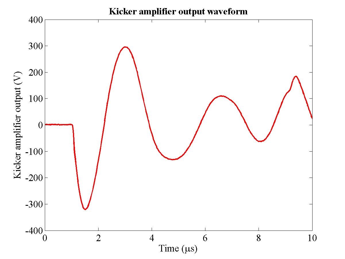
|
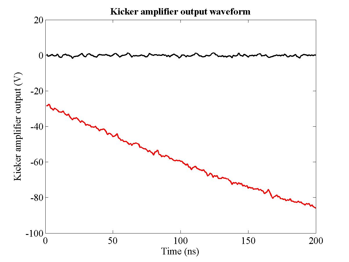
|
||||
| (a) Kicker amplifier output | (b) Close-up of modulated region | ||||
|
|||||
Having tested the normaliser stage of the circuit, the first stage in testing the full FONT system is to the measure the performance of the kicker amplifier. As mentioned in Section 5.3.5, a trigger signal is used to switch on the tubes within the kicker amplifier some 3 µs before the arrival of the beam. This pulse is then modulated with the signal produced by the feedback circuit to drive the kicker magnet and steer the beam. The output pulse of the kicker amplifier is shown in Fig. 5.51(a). This is the raw output of the kicker amplifier without any input from the feedback circuit. A close-up of the region on which the feedback circuit output is superimposed is shown in Fig. 5.51(b).
It is necessary to operate the amplifier in this fashion in order to produce the 2.5 kW power output required to drive the kicker magnet. However, since the nominal amplifier output shown in Fig. 5.51(b) (red trace) is not flat, not only will the whole bunch train experience a net downwards kick due to the overall offset, but the back of the bunch train will receive a larger kick than the front, due to the slope. While a net offset will not affect the overall operation of the feedback system65, it is vital that the slope on the kicker pulse is small compared to the beam offset at the FONT BPM.
| Figure 5.52: The normalised beam position with the kicker amplifier on (blue) and off (black), but receiving no input from the feedback circuit. Note that there is a discernable difference between the two traces as a result of the unmodulated kicker amplifier output. Each trace is the average of 30 beam pulses. |
| Figure 5.53: The difference between the two traces shown in Fig. 5.52. The approximate slope on this difference plot is overlaid in red, with the start and finish of the pulse marked in black. |
The effect of this slope on the beam position is shown in Fig. 5.52. 30 beam pulses were recorded with the kicker amplifier on, but receiving no input from the feedback circuit, and 30 pulses with the kicker amplifier off, with the beam steered upwards by the FONT dipole. There is a clear difference between the normalised beam positions for both cases. By taking the difference between these two pulses, it is possible to analyse the effect of the unmodulated kicker amplifier output on the beam position: this is shown in Fig. 5.53. Although a large peak appears in the middle of this difference plot, it is likely that this peak as a result of the degradation of the beam quality between the two sets of measurements. However, there is also a general trend, marked with a red line, indicating that there is a slope on the beam position as a result of the unmodulated kicker amplifier output. However, the difference between the amplitude of the start and end of this pulse is only 40 mV, while the maximum normalised position seen in Fig. 5.52 is around 800 mV. It is unlikely that an effect on the 5% level such as this will have any adverse effect on the performance of the FONT system.
Finally, the full range of the kicker driver was measured. The kicker amplifier output voltage was measured to saturate at +250 V and −350 V, with an offset of −50 V due to the amplifier output waveform shown in Fig. 5.51(a). This sets the maximum voltage swing at ±300 V: this corresponds to a range of 42 × 10−2 G-m for the FONT dipole. As such, the gain settings of the feedback pre-amp box were set such that the difference signal input to the normaliser stage was between ±1 V for this range for all the data recorded with the feedback system.
| Figure 5.54: The normalised beam position signal for 5 different settings of the FONT dipole. Each trace is the average of 10 beam pulses. |
The next stage was to measure the performance of the FONT system without the delay loop. The results should mirror those of the bench tests presented at the start of Section 5.4.4. By switching on the DC gain signal of the feedback circuit and allowing the feedback circuit to drive the kicker amplifier, it is possible to apply a single loop correction to the measured beam offset. With the delay loop switched off, the beam was steered through five different positions with the FONT dipole, in steps of 8.4 × 10⁻² G-m, with 10 beam pulses recorded at each position. The normalised beam position with the kicker amplifier off is shown in Fig. 5.54. Note that, although there is the same stepping in normalised position as a result of the beam being steered by the FONT dipole, the variation in position along the length of the bunch train is of the same order of magnitude as this stepping. However, this bunch train shape is repeatable: the r.m.s. pulse-to-pulse jitter was observed to be around 10% of the position variation along the length of the train. This means that, although the shape of the bunch train is far from ideal, it is still possible to operate the feedback system, since the kicker is quite capable of moving the beam over a larger range than that of the pulse-to-pulse jitter.
| Figure 5.55: The normalised beam position signal with the feedback circuit on, running at low gain, with the delay loop off. The black lines mark the start and end of the feedback circuit correction. Each trace is the average of 10 beam pulses. |
| Figure 5.56: The normalised beam position signal with the feedback circuit on, running at high gain, with the delay loop off. The black lines mark the start and end of the feedback circuit correction. Each trace is the average of 10 beam pulses. |
The same set of measurements was then repeated using the feedback circuit to attempt a single loop correction of the beam position offset. Two different gain settings — a “low gain” setting of 0.5 V and a “high gain” setting of 1 V — were used for the feedback circuit DC gain, to measure the effect of the circuit gain on the position correction. The low gain response is shown in Fig. 5.55, with the high gain case shown in Fig. 5.56. The effect of the feedback circuit correction can be seen in both cases. For the low gain setting, the beam is steered towards the centre for each of the 5 beam positions. Since the delay loop is not in use, after a single latency period the feedback circuit tries to make a correction based on the corrected part of the bunch train, and the beam is no longer steered as strongly by the kicker magnet.
A similar effect is observed with the high gain setting. In this case, the gain is set closer to the ‘ideal’ setting and, for each of the 5 beam positions, the beam is steered back to the centre of the BPM after a single latency period. Again, after another latency period the feedback circuit stops seeing an offset, and the beam returns to its original position. Even though the beam position for a single pulse shows a great deal of variation along its length, Fig. 5.56 shows a response that is similar to the bench test results shown in Fig. 5.37. Since the feedback system is unable to correct the fine scale position variation, this is exactly the response that one would expect from the feedback system.
It is also possible, using these results, to measure the latency of the full feedback system and use this to set the length of the delay loop for the full system operation (see Section 5.5.5). Using the data shown in Fig. 5.56, the latency is the delay between the start of the pulse and the point at which the feedback correction is applied. Since the delay loop is not in use, this should be approximately the same as the time during which the feedback correction acts, marked by the vertical black lines. The feedback circuit acts after ~75 ns, with the correction also lasting for ~70 ns: the difference in these two figures is likely to be a result both of the granularity of the data and a side effect of the AWG limit66. These figures also match closely the predicted system latency of 67 ns given in Section 5.5.1 (see Table 5.3).
The final stage in the full system test of the FONT system was to carry out the same series of tests described in Section 5.5.4 using the delay loop. The same test parameters were used: 5 different settings of the FONT dipole, space by 8.4 × 10⁻² G-m, with 10 beam pulses recorded at each position. As before, two different gain settings were used: based on the results without the delay loop, the low gain setting should show a slow convergence to a centred beam, while the high gain setting should steer the beam directly to the centre of the BPM and hold it there for the duration of the bunch train.
| Figure 5.57: The normalised beam position signal with the feedback circuit on using the delay loop, running at low gain. The black lines mark the start of successive feedback circuit corrections. Each trace is the average of 10 beam pulses. |
| Figure 5.58: The normalised beam position signal with the feedback circuit on using the delay loop, running at high gain. The black lines mark the start of successive feedback circuit corrections. Each trace is the average of 10 beam pulses. |
The results of the full feedback system test are shown in Figs. 5.57 and 5.58. As before, after a single latency period, the beam offset is registered by the feedback circuit and a correction is applied, reducing the relative offset of each of the 5 beam positions, with a smaller correction applied for the low gain case. As expected, up to the end of the second latency period (at ~205 ns) these results are identical to those of Section 5.5.4 without the delay loop. However, on this occasion the feedback loop switches on after a second latency period and the effect is clear to see. In the low gain case, the feedback loop applies a second correction, steering the beam closer still to the centre of the BPM and narrowing the range of positions of each of the pulses. Even with the added problems caused by the position variation along the length of each bunch train, particularly noticeable with the double peak that appears between 210 and 240 ns, the feedback circuit still manages to reduce the net offset of each beam pulse. This is again similar to the full feedback loop bench test described in Section 5.4.4, with the same stepping behaviour after each latency period apparent (see Fig. 5.41).
For the high gain case, the comparison between Fig. 5.56 and Fig. 5.58 is even more striking than that of the low gain case. This time, the beam position is corrected almost perfectly after a single latency period. Now, when the delay loop switches on, it has to maintain this correction: the close tracking of each of the beam trajectories during the third latency period indicates that it does so. Again, although there are a number of features that appear along the length of the train, the effect of the feedback circuit is to remove the net offset of each bunch train, taking out the offset introduced by the FONT dipole. Close inspection reveals that the correction causes each pulse to overshoot slightly i.e. after 205 ns the high beam is now the lowest and vice versa: this is likely to be a result of using slightly too high a gain in the feedback circuit, leading to an overcorrection. Overall the relative position offset of each of the 5 beam pulses is reduced by at least an order of magnitude. It is clear from each of these results that, within the limits imposed by the intra-train position variation of the beam itself, the FONT system is operating exactly as one would expect.
Finally, an attempt was made to straighten the beam completely by adjusting both the length of the delay loop and the gain of the feedback circuit. The beam was first optimally tuned to remove as much of the intra-train position variation as possible. It was then steered downwards with the FONT dipole and the effect of the FONT system was recorded: 10 beam pulses with the delay loop on, another 10 beam pulses with the delay loop switched off and a final 10 pulses with the FONT system switched off completely. During these tests, the DC and feedback gains were both adjusted to provide the optimal correction; the length of the delay loop was also adjusted slightly to attempt to improve the delay loop correction by cancelling the effects of the large ripples in position variation that occur along the bunch length (see Fig. 5.54) and are propagated through the delay loop.
| Figure 5.59: The effect of the feedback system using optimum gain and delay loop settings. The red trace shows the uncorrected beam position with the FONT system off. The blue trace shows the effect of a single loop correction with the feedback system switching off at ~240 ns. The black trace is the full corrected beam position using the delay loop. Note that the fully corrected beam is completely centred after 250 ns. Each trace is the average of 10 beam pulses. |
The results of this ‘optimum’ test are shown in Fig. 5.59. The three traces shown indicate the beam trajectory for each of the three feedback system operating conditions described above, which could be termed “full” (black trace), “limited” (blue trace) and “off” (red trace). Two features are once again clear from this figure, both related to the activation of different parts of the feedback system. The first is the point at which the initial correction is applied, at 170 ns: the two corrected beam trajectories are clearly steered upwards, back towards the BPM centre. However, the plateau from 190 to 230 ns indicates that the correction is not perfect, since the beam is not steered exactly to the centre of the BPM: this was an artificially imposed condition, designed to show the effect of the delay loop signal on the position correction.
The second feature is the trajectory of the fully corrected beam after 240 ns. While the “limited” beam trajectory slowly regains its offset, as the feedback system tries to make a correction based on the smaller offset seen between 190 and 230 ns, the “full” beam trajectory shows no such features: in fact, it shows no features at all. This indicates that the beam has been completely centred for the last ~50 ns of the bunch train. This plot shows a remarkable similarity to the bench tests carried out under ideal conditions (cf. Fig. 5.41). However, unlike the bench test the input data to the feedback system is real beam data, with a real-time correction applied to an actual beam, rather than just a simulated signal. Yet the correction applied by the feedback system is just as effective. The figure compares very favourably to the results of the IPFB simulations detailed in Section 3.4, particularly those shown in Fig. 3.20. The conclusion is therefore that the feedback system functions exactly as designed, since it is able to iteratively correct a beam offset within a single bunch train.
52 Magnets identified and located by Cherrill Spencer and released by Jim Allen.
53 Data on NLCTA dipole and quadrupole magnet gradients taken from the SCP.
54 It is therefore likely, since the shape of the curves in Figs. 4.57 and 5.14 for both the sum signal and toroid is so similar, that the signal degradation is a result of the aperture of the FONT BPM. Since the transmission profile of all the measurements shows no plateau, the likelihood is that the beam is larger than the FONT BPM beampipe diameter.
55 Magnets identified and located by Paul Stephens and Marc Ross and released by Jim Allen.
56 The designation of pairs of connectors as ‘input’ and ‘output’ is essentially redundant, and dependent only on the pair to which the supply voltage is connected: there is no mechanical or electrical difference between any of the four connectors. In practice, only one input and output connector is used: the kicker assembly has four connectors, rather than two, to allow the connection of a second power supply to allow a greater voltage to be applied.
57
58 Q-switch power supply, ID 102-002, designed, built and supplied for FONT's use by Dave Brown at SLAC.
59 A Pockels cell is a high speed optical switch that uses a voltage to modulate the refractive index of a crystal. A fast, high voltage power supply is required to change the field applied to the crystal at high speed, allowing fast switching of an optical source, such as a laser.
60 A gain of 5 rather than 4 is used for the output amplifier to take account of the inherent gain of each of the multiplier chips of 0.95, as well as any transmission loss.
61 DC supply board machined and assembled by Matt Sorgenfrei at SLAC.
62 NLCTA control and DAQ is split between two micro's: TA01, primarily responsible for the front half of the accelerator, up to quad QD1110, and TA02, used for the rear section of the accelerator.
63 In truth, the Z offset adjust is not necessary, since the feedback circuit itself removes any DC offset through its AC-coupled inputs (see Fig. 5.24). However, the addition of such adjusts was neither time consuming nor detrimental to the operation of the circuit, so they were included in the same fashion as before.
64 Beam length measurements taken from the SCP.
65 The net offset merely means that the beam is displaced slightly further downwards than if the FONT dipole were operating alone. Since the kicker and dipole magnets occupy the same location, the net effect is as if the dipole had been steered slightly downwards. Any such offset can therefore be taken out with the dipole.
66 To prevent the AWG 1/Q signal overdriving the input of the normaliser stage, the AWG output is limited to 2 V. This means that, at the start of the beam pulse, when the beam charge is low, the AWG pulse is artifically low. This limits the usable pulse length to that with a large enough beam charge, and results in approximately the first 5 ns of the pulse being unusable. The same is also true for the end of the pulse.
© Simon Jolly 2003